LM2853
LM2853 3A 550 kHz Synchronous SIMPLE SWITCHER® Buck Regulator
Literature Number: SNVS459
�LM2853
3A 550 kHz Synchronous SIMPLE SWITCHER ® Buck
Regulator
General Description
Features
SWITCHER ®
The LM2853 synchronous SIMPLE
buck regulator is a 550 kHz step-down switching voltage regulator
capable of driving up to a 3A load with excellent line and load
regulation. The LM2853 accepts an input voltage between
3.0V and 5.5V and delivers a customizable output voltage
that is factory programmable from 0.8V to 3.3V in 100mV
increments. Internal type-three compensation enables a low
component count solution and greatly simplifies external
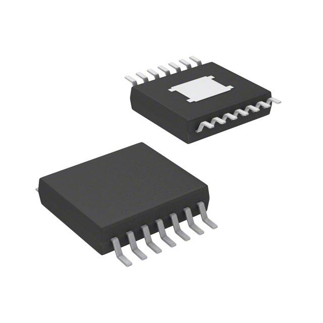
component selection. The exposed-pad TSSOP-14 package
enhances the thermal performance of the LM2853.
n Input voltage range of 3.0V to 5.5V
n Factory EEPROM set output voltages from 0.8V to 3.3V
in 100 mV increments
n Maximum load current of 3A
n Voltage Mode Control
n Internal type-three compensation
n Switching frequency of 550 kHz
n Low standby current of 12 µA
n Internal 40 mΩ MOSFET switches
n Standard voltage options
0.8/1.0/1.2/1.5/1.8/2.5/3.0/3.3 volts
n Exposed pad TSSOP-14 package
Applications
n Low voltage point of load regulation
n Local solution for FPGA/DSP/ASIC core power
n Broadband networking and communications
infrastructure
Typical Application Circuit
20201502
Efficiency vs Load Current (VOUT = 3.3V)
20201501
SIMPLE SWITCHER ® is a Registered Trademark of National Semiconductor Corporation.
© 2006 National Semiconductor Corporation
DS202015
www.national.com
LM2853 3A 550 kHz Synchronous SIMPLE SWITCHER ® Buck Regulator
October 2006
�LM2853
Connection Diagram
20201503
Ordering Information
Order Number
LM2853MH-0.8
LM2853MHX-0.8
LM2853MH-1.0
LM2853MHX-1.0
LM2853MH-1.2
LM2853MHX-1.2
LM2853MH-1.5
LM2853MHX-1.5
LM2853MH-1.8
LM2853MHX-1.8
LM2853MH-2.5
LM2853MHX-2.5
LM2853MH-3.0
LM2853MHX-3.0
LM2853MH-3.3
LM2853MHX-3.3
Voltage
Option
Package
Marking
0.8
LM2853-0.8
1.0
LM2853-1.0
1.2
LM2853-1.2
1.5
LM2853-1.5
1.8
LM2853-1.8
2.5
LM2853-2.5
3.0
LM2853-3.0
3.3
LM2853-3.3
Package Type
Package
Drawing
Supplied As
94 Units, Rail
2500 Units, Tape and Reel
94 Units, Rail
2500 Units, Tape and Reel
94 Units, Rail
2500 Units, Tape and Reel
94 Units, Rail
TSSOP-14 exposed
pad
MXA14A
2500 Units, Tape and Reel
94 Units, Rail
2500 Units, Tape and Reel
94 Units, Rail
2500 Units, Tape and Reel
94 Units, Rail
2500 Units, Tape and Reel
94 Units, Rail
2500 Units, Tape and Reel
Note: Contact factory for other voltage options.
Pin Descriptions
Pin #
Name
1
AVIN
2
EN
3
SGND
Enable.
Low noise ground.
4
SS
Soft-Start Pin.
5
NC
No Connect. This pin must be tied to ground.
6,7
PVIN
8,9
SW
10,11
PGND
12,13
NC
14
SNS
Exposed Pad
EP
www.national.com
Function
Input Voltage for Control Circuitry.
Input Voltage for Power Circuitry.
Switch Pin.
Power Ground.
No-Connect. These pins must be tied to ground.
Output Voltage Sense Pin.
The exposed pad is internally connected to GND, but it cannot be
used as the primary GND connection. The exposed pad should be
soldered to an external GND plane.
2
�14-Pin Exposed Pad TSSOP Package
If Military/Aerospace specified devices are required,
please contact the National Semiconductor Sales Office/
Distributors for availability and specifications.
AVIN, PVIN, EN, SNS, SW, SS
Infrared (15 sec)
220˚C
Vapor Phase (60 sec)
215˚C
Soldering (10 sec)
260˚C
−0.3V to 6.0V
ESD Susceptibility (Note 2)
2kV
Operating Ratings (Note 1)
Power Dissipation
Internally Limited
Storage Temperature Range
−65˚C to +150˚C
PVIN to GND
150˚C
AVIN to GND
Maximum Junction Temp.
1.5V to 5.5V
3.0V to 5.5V
Junction Temperature
−40˚C to +125˚C
Electrical Characteristics Specifications with standard typeface are for TJ = 25˚C, and those in bold face
type apply over the full Junction Temperature Range (−40˚C to 125˚C). Minimum and Maximum limits are guaranteed through
test, design or statistical correlation. Typical values represent the most likely parametric norm at TJ = 25˚C and are provided
for reference purposes only. Unless otherwise specified AVIN = PVIN = 5V.
Symbol
Parameter
Conditions
Min
Typ
Max
VOUT = 0.8V option
0.782
0.8
0.818
VOUT = 1.0V option
0.9775
1.0
1.0225
VOUT = 1.2V option
1.1730
1.2
1.227
Units
SYSTEM PARAMETERS
VOUT
∆VOUT/∆AVIN
Voltage Tolerance (Note 3)
Line Regulation (Note 3)
VOUT = 1.5V option
1.4663
1.5
1.5337
VOUT = 1.8V option
1.7595
1.8
1.8405
VOUT = 2.5V option
2.4437
2.5
2.5563
VOUT = 3.0V option
2.9325
3.0
3.0675
VOUT = 3.3V option
3.2257
V
3.3
3.3743
VOUT = 0.8V, 1.0V, 1.2V, 1.5V,
1.8V or 2.5V
3.0V ≤ AVIN ≤ 5.5V
0.2
1.1
%
VOUT = 3.0V or 3.3V
3.5V ≤ AVIN ≤ 5.5V
0.2
1.1
%
∆VOUT/∆IO
Load Regulation
Normal operation
VON
UVLO Threshold (AVIN)
Rising
Falling Hysteresis
RDS(ON)-P
PFET On Resistance
Isw = 3A
RDS(ON)-N
NFET On Resistance
Isw = 3A
RSS
Soft-Start Resistance
ICL
Peak Current Limit Threshold
IQ
Operating Current
Non-switching
ISD
Shutdown Quiescent Current
EN = 0V
RSNS
Sense Pin Resistance
2
50
3.6
mV/A
2.47
3.0
V
155
260
mV
40
120
mΩ
32
100
mΩ
450
kΩ
5
A
0.85
2
12
50
432
mA
µA
kΩ
PWM
fosc
Switching Frequency
Drange
Duty Cycle Range
.
325
550
0
725
kHz
100
%
ENABLE CONTROL (Note 4)
VIH
EN Pin Minimum High Input
VIL
EN Pin Maximum Low Input
IEN
EN Pin Pullup Current
75
% of
AVIN
25
EN = 0V
1.5
3
% of
AVIN
µA
www.national.com
LM2853
Absolute Maximum Ratings (Note 1)
�LM2853
Electrical Characteristics Specifications with standard typeface are for TJ = 25˚C, and those in bold face type
apply over the full Junction Temperature Range (−40˚C to 125˚C). Minimum and Maximum limits are guaranteed through test,
design or statistical correlation. Typical values represent the most likely parametric norm at TJ = 25˚C and are provided for
reference purposes only. Unless otherwise specified AVIN = PVIN = 5V. (Continued)
Symbol
Parameter
Conditions
Min
Typ
Max
Units
THERMAL CONTROLS
TSD
Thermal Shutdown Threshold
165
˚C
TSD-HYS
Hysteresis for Thermal
Shutdown
10
˚C
38
˚C/W
THERMAL RESISTANCE
θJA
Junction to Ambient
MXA14A
Note 1: Absolute maximum ratings indicate limits beyond which damage to the device may occur. Operating Range indicates conditions for which the device is
intended to be functional, but does not guarantee specific performance limits. For guaranteed specifications and test conditions, see the Electrical Characteristics.
Note 2: The human body model is a 100 pF capacitor discharged through a 1.5 kΩ resistor into each pin. Test Method is per JESD22-AI14.
Note 3: VOUT measured in a non-switching, closed-loop configuration at the SNS pin.
Note 4: The enable pin is internally pulled up, so the LM2853 is automatically enabled unless an external enable voltage is applied.
www.national.com
4
�Unless otherwise specified, the following conditions apply: VIN
= AVIN = PVIN = 5V, TJ = 25˚C.
Efficiency vs. ILOAD
VOUT = 1.8V
NFET RDS(ON) vs. Temperature
20201507
20201505
Efficiency vs. ILOAD
VOUT = 2.5V
PFET RDS(ON) vs. Temperature
20201509
20201504
Efficiency vs. ILOAD
VOUT = 3.3V
Switching Frequency vs. Temperature
20201508
20201506
5
www.national.com
LM2853
Typical Performance Characteristics
�LM2853
Typical Performance Characteristics Unless otherwise specified, the following conditions apply: VIN
= AVIN = PVIN = 5V, TJ = 25˚C. (Continued)
IQ vs. VIN and Temperature
ISD vs. VIN and Temperature
20201510
www.national.com
20201511
6
�LM2853
Block Diagram
20201512
Applications Information
load regulation and transient performance, the use of a small
1 µF ceramic capacitor is also recommended as a local
bypass for the AVIN pin.
The LM2853 is a DC-DC buck regulator belonging to National Semiconductor’s synchronous SIMPLE SWITCHER ®
family. Integration of the PWM controller, power switches
and compensation network greatly reduces the component
count required to implement a switching power supply. A
typical application requires only four components: an input
capacitor, a soft-start capacitor, an output filter capacitor and
an output filter inductor.
SOFT-START CAPACITOR (CSS)
The DAC that sets the reference voltage of the error amplifier sources a current through a resistor to set the reference
voltage. The reference voltage is one half of the output
voltage of the switcher due to the 200 kΩ divider connected
to the SNS pin. Upon start-up, the output voltage of the
switcher tracks the reference voltage with a two to one ratio
as the DAC current charges the capacitance connected to
the reference voltage node. Internal capacitance of 20 pF is
permanently attached to the reference voltage node which is
also connected to the soft start pin, SS. Adding a soft-start
capacitor externally increases the time it takes for the output
voltage to reach its final level. The charging time required for
the reference voltage can be estimated using the RC time
constant of the DAC resistor and the capacitance connected
to the SS pin. Three RC time constant periods are needed
for the reference voltage to reach 95% of its final value. The
actual start up time will vary with differences in the DAC
resistance and higher-order effects.
If little or no soft-start capacitance is connected, then the
start up time may be determined by the time required for the
current limit current to charge the output filter capacitance.
The capacitor charging equation I = C∆V/∆t can be used to
estimate the start-up time in this case. For example, a part
with a 3V output, a 100 µF output capacitance and a 5A
current limit threshold would require a time of 60 µs:
INPUT CAPACITOR (CIN)
Fast switching of large currents in the buck converter places
a heavy demand on the voltage source supplying PVIN. The
input capacitor, CIN, supplies extra charge when the switcher
needs to draw a burst of current from the supply. The RMS
current rating and the voltage rating of the CIN capacitor are
therefore important in the selection of CIN. The RMS current
specification can be approximated by:
where D is the duty cycle, VOUT/VIN. CIN also provides
filtering of the supply. Trace resistance and inductance degrade the benefits of the input capacitor, so CIN should be
placed very close to PVIN in the layout. A 22 µF or 47 µF
ceramic capacitor is typically sufficient for CIN. In parallel
with the large input capacitance a smaller capacitor should
be added such as a 1 µF ceramic for higher frequency
filtering. Ceramic capacitors with high quality dielectrics such
as X5R or X7R should be used to provide a constant capacitance across temperature and line variations. For improved
7
www.national.com
�LM2853
Applications Information
voltage the output reached during the short circuit event. The
range of soft-start capacitors is therefore restricted to values
1 nF to 50 nF.
(Continued)
COMPENSATION
The LM2853 provides a highly integrated solution to power
supply design. The compensation of the LM2853, which is
type-three, is included on-chip. The benefit of integrated
compensation is straight-forward, simple power supply design. Since the output filter capacitor and inductor values
impact the compensation of the control loop, the range of LO,
CO and CESR values is restricted in order to ensure stability.
Since it is undesirable for the power supply to start up in
current limit, a soft-start capacitor must be chosen to force
the LM2853 to start up in a more controlled fashion based on
the charging of the soft-start capacitance. In this example,
suppose a 3 ms start time is desired. Three time constants
are required for charging the soft-start capacitor to 95% of
the final reference voltage. So in this case RC = 1 ms. The
DAC resistor, R, is 450 kΩ so C can be calculated to be 2.2
nF. A 2.2 nF ceramic capacitor can be chosen to yield
approximately a 3 ms start-up time.
OUTPUT FILTER VALUES
Table 1 details the recommended inductor and capacitor
ranges for the LM2853 that are suggested for various typical
output voltages. Values slightly different than those recommended may be used, however the phase margin of the
power supply may be degraded. For best performance when
output voltage ripple is a concern, ESR values near the
minimum of the recommended range should be paired with
capacitance values near the maximum. If a minimum output
voltage ripple solution from a 5V input voltage is desired, a
6.8 µH inductor can be paired with a 220 µF (50 mΩ)
capacitor without degraded phase margin.
SOFT-START CAPACITOR (CSS) AND FAULT
CONDITIONS
Various fault conditions such as short circuit and UVLO of
the LM2853 activate internal circuitry designed to control the
voltage on the soft-start capacitor. For example, during a
short circuit current limit event, the output voltage typically
falls to a low voltage. During this time, the soft-start voltage
is forced to track the output so that once the short is removed, the LM2853 can restart gracefully from whatever
TABLE 1. Recommended LO and CO Values
LO (µH)
CO (µF)
CESR (mΩ)
VOUT (V)
VIN (V)
Min
Max
Min
Max
Min
Max
0.8
5
4.7
6.8
120
220
70
100
0.8
3.3
4.7
4.7
150
220
50
100
1
5
4.7
6.8
120
220
70
100
1
3.3
4.7
4.7
150
220
50
100
1.2
5
4.7
6.8
120
220
70
100
1.2
3.3
4.7
4.7
120
220
60
100
1.5
5
4.7
6.8
120
220
70
100
1.5
3.3
4.7
4.7
120
220
60
100
1.8
5
4.7
6.8
120
220
70
120
1.8
3.3
4.7
4.7
100
220
70
120
2.5
5
4.7
6.8
120
220
70
150
2.5
3.3
4.7
4.7
100
220
80
150
3.0
5
4.7
6.8
120
220
70
150
3.0
3.3
4.7
4.7
100
220
80
150
3.3
5
4.7
6.8
120
220
70
150
www.national.com
8
�LM2853
Applications Information
(Continued)
CHOOSING AN INDUCTANCE VALUE
The current ripple present in the output filter inductor is
determined by the input voltage, output voltage, switching
frequency and inductance according to the following equation:
The maximum inductor current for a 3A load would therefore
be 3A plus 177 mA, 3.177A. As shown in the ripple equation,
the current ripple is inversely proportional to inductance.
OUTPUT FILTER INDUCTORS
Once the inductance value is chosen, the key parameter for
selecting the output filter inductor is its saturation current
(ISAT) specification. Typically ISAT is given by the manufacturer as the current at which the inductance of the coil falls to
a certain percentage of the nominal inductance. The ISAT of
an inductor used in an application should be greater than the
maximum expected inductor current to avoid saturation. Below is a table of inductors that are suitable in LM2853
applications.
where ∆IL is the peak to peak current ripple, D is the duty
cycle VOUT/VIN, VIN is the input voltage applied to the output
stage, VOUT is the output voltage of the switcher, f is the
switching frequency and LO is the inductance of the output
filter inductor. Knowing the current ripple is important for
inductor selection since the peak current through the inductor is the load current plus one half the ripple current. Care
must be taken to ensure the peak inductor current does not
reach a level high enough to trip the current limit circuitry of
the LM2853. As an example, consider a 5V to 1.2V conversion and a 550 kHz switching frequency. According to Table
1, a 4.7 µH inductor may be used. Calculating the expected
peak-to-peak ripple,
TABLE 2. Recommended Inductors
Inductance
Part Number
Vendor
4.7 µF
DO3308P-472ML
Coilcraft
4.7 µF
DO3316P-472ML
Coilcraft
4.7 µF
MSS1260-472ML
Coilcraft
5.2 µF
MSS1038-522NL
Coilcraft
5.6 µF
MSS1260-562ML
Coilcraft
6.8 µF
DO3316P-682ML
Coilcraft
6.8 µF
MSS1260-682ML
Coilcraft
OUTPUT FILTER CAPACITORS
The recommended capacitors that may be used in the output
filter with the LM2853 are limited in value and ESR range
according to Table 1.
Below are some examples of capacitors that can typically be
used in an LM2853 application.
TABLE 3. Recommended Capacitors
Capacitance (µF)
Part Number
Chemistry
Vendor
100
594D107X_010C2T
Tantalum
Vishay-Sprague
100
593D107X_010D2_E3
Tantalum
Vishay-Sprague
100
TPSC107M006#0075
Tantalum
AVX
100
NOSD107M006#0080
Niobium Oxide
AVX
100
NOSC107M004#0070
Niobium Oxide
AVX
120
594D127X_6R3C2T
Tantalum
Vishay-Sprague
150
594D157X_010C2T
Tantalum
Vishay-Sprague
150
595D157X_010D2T
Tantalum
Vishay-Sprague
150
591D157X_6R3C2_20H
Tantalum
Vishay-Sprague
150
TPSD157M006#0050
Tantalum
AVX
AVX
150
TPSC157M004#0070
Tantalum
150
NOSD157M006#0070
Niobium Oxide
AVX
220
594D227X_6R3D2T
Tantalum
Vishay-Sprague
220
591D227X_6R3D2_20H
Tantalum
Vishay-Sprague
220
591D227X_010D2_20H
Tantalum
Vishay-Sprague
220
593D227X_6R3D2_E3
Tantalum
Vishay-Sprague
9
www.national.com
�LM2853
Applications Information
(Continued)
TABLE 3. Recommended Capacitors (Continued)
Capacitance (µF)
Part Number
Chemistry
220
TPSD227M006#0050
Tantalum
AVX
220
NOSD227M0040060
Niobium Oxide
AVX
SPLIT-RAIL OPERATION
Vendor
components need to be chosen based on the value of PVIN.
For PVIN levels lower than 3.3V, use output filter component
values recommended for 3.3V. PVIN must always be equal
to or less than AVIN.
The LM2853 can be powered using two separate voltages
for AVIN and PVIN. AVIN is the supply for the control logic;
PVIN is the supply for the power FETs. The output filter
20201513
SWITCH NODE PROTECTION
The LM2853 includes protection circuitry that monitors the
voltage on the switch pin. Under certain fault conditions,
switching is disabled in order to protect the switching devices. One side effect of the protection circuitry may be
observed when power to the LM2853 is applied with no or
light load on the output. The output will regulate to the rated
voltage, but no switching may be observed. As soon as the
output is loaded, the LM2853 will begin normal switching
operation.
tween all ground connections.
3.
The sense pin connection should be made as close to
the load as possible so that the voltage at the load is the
expected regulated value. The sense line should not run
too close to nodes with high dV/dt or dl/dt (such as the
switch node) to minimize interference.
4. The switch node connections should be low resistance
to reduce power losses. Low resistance means the trace
between the switch pin and the inductor should be wide.
However, the area of the switch node should not be too
large since EMI increases with greater area. So connect
the inductor to the switch pin with a short, but wide trace.
Other high current connections in the application such
as PVIN and VOUT assume the same trade off between
low resistance and EMI.
LAYOUT GUIDELINES
These are several guidelines to follow while designing the
PCB layout for an LM2853 application.
1. The input bulk capacitor, CIN, should be placed very
close to the PVIN pin to keep the resistance as low as
possible between the capacitor and the pin. High current
levels will be present in this connection.
2. All ground connections must be tied together. Use a
broad ground plane, for example a completely filled back
plane, to establish the lowest resistance possible be-
5.
Allow area under the chip to solder the entire exposed
die attach pad to ground for improved thermal performance. Lab measurements also show improved regulation performance when the exposed pad is well
grounded.
LM2853 Example Circuit Schematic
20201514
FIGURE 1.
www.national.com
10
�LM2853
LM2853 Example Circuit Schematic
(Continued)
Bill of Materials for 5V to 3.3V Conversion
ID
Part Number
Type
Size
Parameters
Qty
U1
LM2853MH-3.3
3A Buck
ETSSOP-14
3.3V
1
Vendor
NSC
CIN
GRM31CR60J476ME19
Capacitor
1206
47 µF
1
Murata
CBYP
GRM21BR71C105KA01
Capacitor
0805
1 µF
1
Murata
CSS
VJ0805Y222KXXA
Capacitor
0603
2.2 nF
1
Vishay-Vitramon
LO
DO3316P-682
Inductor
DO3316P
6.8 µH
1
Coilcraft
CO
594D127X06R3C2T
Capacitor
C Case
120µF
(85mΩ)
1
Vishay-Sprague
Bill of Materials for 3.3V to 1.2V Conversion
ID
Part Number
Type
Size
Parameters
Qty
Vendor
U1
LM2853MH-1.2
3A Buck
ETSSOP-14
1.2V
1
NSC
CIN
GRM31CR60J476ME19
Capacitor
1206
47 µF
1
Murata
CBYP
GRM21BR71C105KA01
Capacitor
0805
1 µF
1
Murata
CSS
VJ0805Y222KXXA
Capacitor
0603
2.2 nF
1
Vishay-Vitramon
LO
DO3316P-472
Inductor
DO3316P
4.7 µH
1
Coilcraft
CO
NOSD157M006R0070
Capacitor
D Case
150 µF
(70 mΩ)
1
AVX
11
www.national.com
�PACKAGE OPTION ADDENDUM
www.ti.com
23-Sep-2013
PACKAGING INFORMATION
Orderable Device
Status
(1)
Package Type Package Pins Package
Drawing
Qty
LM2853MH-0.8
ACTIVE
HTSSOP
PWP
14
LM2853MH-0.8/NOPB
ACTIVE
HTSSOP
PWP
14
LM2853MH-1.0
ACTIVE
HTSSOP
PWP
14
LM2853MH-1.0/NOPB
ACTIVE
HTSSOP
PWP
14
LM2853MH-1.2
ACTIVE
HTSSOP
PWP
14
LM2853MH-1.2/NOPB
ACTIVE
HTSSOP
PWP
14
LM2853MH-1.5
ACTIVE
HTSSOP
PWP
14
LM2853MH-1.5/NOPB
ACTIVE
HTSSOP
PWP
14
LM2853MH-1.8
ACTIVE
HTSSOP
PWP
LM2853MH-1.8/NOPB
ACTIVE
HTSSOP
LM2853MH-2.5
ACTIVE
LM2853MH-2.5/NOPB
Eco Plan
Lead/Ball Finish
(2)
MSL Peak Temp
Op Temp (°C)
Device Marking
(3)
(4/5)
TBD
Call TI
Call TI
-40 to 125
LM2853
-0.8
Green (RoHS
& no Sb/Br)
CU SN
Level-1-260C-UNLIM
-40 to 125
LM2853
-0.8
TBD
Call TI
Call TI
-40 to 125
LM2853
-1.0
Green (RoHS
& no Sb/Br)
CU SN
Level-1-260C-UNLIM
-40 to 125
LM2853
-1.0
TBD
Call TI
Call TI
-40 to 125
LM2853
-1.2
Green (RoHS
& no Sb/Br)
CU SN
Level-1-260C-UNLIM
-40 to 125
LM2853
-1.2
TBD
Call TI
Call TI
-40 to 125
LM2853
-1.5
94
Green (RoHS
& no Sb/Br)
CU SN
Level-1-260C-UNLIM
-40 to 125
LM2853
-1.5
14
94
TBD
Call TI
Call TI
-40 to 125
LM2853
-1.8
PWP
14
94
Green (RoHS
& no Sb/Br)
CU SN
Level-1-260C-UNLIM
-40 to 125
LM2853
-1.8
HTSSOP
PWP
14
TBD
Call TI
Call TI
-40 to 125
LM2853
-2.5
ACTIVE
HTSSOP
PWP
14
Green (RoHS
& no Sb/Br)
CU SN
Level-1-260C-UNLIM
-40 to 125
LM2853
-2.5
LM2853MH-3.0
ACTIVE
HTSSOP
PWP
14
TBD
Call TI
Call TI
-40 to 125
LM2853
-3.0
LM2853MH-3.0/NOPB
ACTIVE
HTSSOP
PWP
14
94
Green (RoHS
& no Sb/Br)
CU SN
Level-1-260C-UNLIM
-40 to 125
LM2853
-3.0
LM2853MH-3.3
ACTIVE
HTSSOP
PWP
14
94
TBD
Call TI
Call TI
-40 to 125
LM2853
-3.3
LM2853MH-3.3/NOPB
ACTIVE
HTSSOP
PWP
14
94
Green (RoHS
& no Sb/Br)
CU SN
Level-1-260C-UNLIM
-40 to 125
LM2853
-3.3
LM2853MHX-0.8
ACTIVE
HTSSOP
PWP
14
TBD
Call TI
Call TI
-40 to 125
LM2853
-0.8
94
94
94
94
Addendum-Page 1
Samples
�PACKAGE OPTION ADDENDUM
www.ti.com
Orderable Device
23-Sep-2013
Status
(1)
Package Type Package Pins Package
Drawing
Qty
LM2853MHX-0.8/NOPB
ACTIVE
HTSSOP
PWP
14
LM2853MHX-1.0
ACTIVE
HTSSOP
PWP
14
LM2853MHX-1.0/NOPB
ACTIVE
HTSSOP
PWP
14
LM2853MHX-1.2
ACTIVE
HTSSOP
PWP
14
LM2853MHX-1.2/NOPB
ACTIVE
HTSSOP
PWP
14
LM2853MHX-1.5
ACTIVE
HTSSOP
PWP
14
LM2853MHX-1.5/NOPB
ACTIVE
HTSSOP
PWP
14
LM2853MHX-1.8
ACTIVE
HTSSOP
PWP
14
LM2853MHX-1.8/NOPB
ACTIVE
HTSSOP
PWP
14
LM2853MHX-2.5
ACTIVE
HTSSOP
PWP
14
LM2853MHX-2.5/NOPB
ACTIVE
HTSSOP
PWP
14
LM2853MHX-3.0
ACTIVE
HTSSOP
PWP
14
LM2853MHX-3.0/NOPB
ACTIVE
HTSSOP
PWP
14
LM2853MHX-3.3
ACTIVE
HTSSOP
PWP
14
LM2853MHX-3.3/NOPB
ACTIVE
HTSSOP
PWP
14
2500
2500
2500
2500
2500
2500
2500
2500
Eco Plan
Lead/Ball Finish
(2)
MSL Peak Temp
Op Temp (°C)
Device Marking
(3)
(4/5)
Green (RoHS
& no Sb/Br)
CU SN
Level-1-260C-UNLIM
-40 to 125
LM2853
-0.8
TBD
Call TI
Call TI
-40 to 125
LM2853
-1.0
Green (RoHS
& no Sb/Br)
CU SN
Level-1-260C-UNLIM
-40 to 125
LM2853
-1.0
TBD
Call TI
Call TI
-40 to 125
LM2853
-1.2
Green (RoHS
& no Sb/Br)
CU SN
Level-1-260C-UNLIM
-40 to 125
LM2853
-1.2
TBD
Call TI
Call TI
-40 to 125
LM2853
-1.5
Green (RoHS
& no Sb/Br)
CU SN
Level-1-260C-UNLIM
-40 to 125
LM2853
-1.5
TBD
Call TI
Call TI
-40 to 125
LM2853
-1.8
Green (RoHS
& no Sb/Br)
CU SN
Level-1-260C-UNLIM
-40 to 125
LM2853
-1.8
TBD
Call TI
Call TI
-40 to 125
LM2853
-2.5
Green (RoHS
& no Sb/Br)
CU SN
Level-1-260C-UNLIM
-40 to 125
LM2853
-2.5
TBD
Call TI
Call TI
-40 to 125
LM2853
-3.0
Green (RoHS
& no Sb/Br)
CU SN
Level-1-260C-UNLIM
-40 to 125
LM2853
-3.0
TBD
Call TI
Call TI
-40 to 125
LM2853
-3.3
Green (RoHS
& no Sb/Br)
CU SN
Level-1-260C-UNLIM
-40 to 125
LM2853
-3.3
(1)
The marketing status values are defined as follows:
ACTIVE: Product device recommended for new designs.
LIFEBUY: TI has announced that the device will be discontinued, and a lifetime-buy period is in effect.
NRND: Not recommended for new designs. Device is in production to support existing customers, but TI does not recommend using this part in a new design.
PREVIEW: Device has been announced but is not in production. Samples may or may not be available.
OBSOLETE: TI has discontinued the production of the device.
Addendum-Page 2
Samples
�PACKAGE OPTION ADDENDUM
www.ti.com
23-Sep-2013
(2)
Eco Plan - The planned eco-friendly classification: Pb-Free (RoHS), Pb-Free (RoHS Exempt), or Green (RoHS & no Sb/Br) - please check http://www.ti.com/productcontent for the latest availability
information and additional product content details.
TBD: The Pb-Free/Green conversion plan has not been defined.
Pb-Free (RoHS): TI's terms "Lead-Free" or "Pb-Free" mean semiconductor products that are compatible with the current RoHS requirements for all 6 substances, including the requirement that
lead not exceed 0.1% by weight in homogeneous materials. Where designed to be soldered at high temperatures, TI Pb-Free products are suitable for use in specified lead-free processes.
Pb-Free (RoHS Exempt): This component has a RoHS exemption for either 1) lead-based flip-chip solder bumps used between the die and package, or 2) lead-based die adhesive used between
the die and leadframe. The component is otherwise considered Pb-Free (RoHS compatible) as defined above.
Green (RoHS & no Sb/Br): TI defines "Green" to mean Pb-Free (RoHS compatible), and free of Bromine (Br) and Antimony (Sb) based flame retardants (Br or Sb do not exceed 0.1% by weight
in homogeneous material)
(3)
MSL, Peak Temp. -- The Moisture Sensitivity Level rating according to the JEDEC industry standard classifications, and peak solder temperature.
(4)
There may be additional marking, which relates to the logo, the lot trace code information, or the environmental category on the device.
(5)
Multiple Device Markings will be inside parentheses. Only one Device Marking contained in parentheses and separated by a "~" will appear on a device. If a line is indented then it is a continuation
of the previous line and the two combined represent the entire Device Marking for that device.
Important Information and Disclaimer:The information provided on this page represents TI's knowledge and belief as of the date that it is provided. TI bases its knowledge and belief on information
provided by third parties, and makes no representation or warranty as to the accuracy of such information. Efforts are underway to better integrate information from third parties. TI has taken and
continues to take reasonable steps to provide representative and accurate information but may not have conducted destructive testing or chemical analysis on incoming materials and chemicals.
TI and TI suppliers consider certain information to be proprietary, and thus CAS numbers and other limited information may not be available for release.
In no event shall TI's liability arising out of such information exceed the total purchase price of the TI part(s) at issue in this document sold by TI to Customer on an annual basis.
Addendum-Page 3
�PACKAGE MATERIALS INFORMATION
www.ti.com
23-Sep-2013
TAPE AND REEL INFORMATION
*All dimensions are nominal
Device
Package Package Pins
Type Drawing
SPQ
Reel
Reel
A0
Diameter Width (mm)
(mm) W1 (mm)
B0
(mm)
K0
(mm)
P1
(mm)
W
Pin1
(mm) Quadrant
LM2853MHX-0.8/NOPB HTSSOP
PWP
14
2500
330.0
12.4
6.95
8.3
1.6
8.0
12.0
Q1
LM2853MHX-1.0/NOPB HTSSOP
PWP
14
2500
330.0
12.4
6.95
8.3
1.6
8.0
12.0
Q1
LM2853MHX-1.2/NOPB HTSSOP
PWP
14
2500
330.0
12.4
6.95
8.3
1.6
8.0
12.0
Q1
LM2853MHX-1.5/NOPB HTSSOP
PWP
14
2500
330.0
12.4
6.95
8.3
1.6
8.0
12.0
Q1
LM2853MHX-1.8/NOPB HTSSOP
PWP
14
2500
330.0
12.4
6.95
8.3
1.6
8.0
12.0
Q1
LM2853MHX-2.5/NOPB HTSSOP
PWP
14
2500
330.0
12.4
6.95
8.3
1.6
8.0
12.0
Q1
LM2853MHX-3.0/NOPB HTSSOP
PWP
14
2500
330.0
12.4
6.95
8.3
1.6
8.0
12.0
Q1
LM2853MHX-3.3/NOPB HTSSOP
PWP
14
2500
330.0
12.4
6.95
8.3
1.6
8.0
12.0
Q1
Pack Materials-Page 1
�PACKAGE MATERIALS INFORMATION
www.ti.com
23-Sep-2013
*All dimensions are nominal
Device
Package Type
Package Drawing
Pins
SPQ
Length (mm)
Width (mm)
Height (mm)
LM2853MHX-0.8/NOPB
HTSSOP
PWP
14
2500
367.0
367.0
35.0
LM2853MHX-1.0/NOPB
HTSSOP
PWP
14
2500
367.0
367.0
35.0
LM2853MHX-1.2/NOPB
HTSSOP
PWP
14
2500
367.0
367.0
35.0
LM2853MHX-1.5/NOPB
HTSSOP
PWP
14
2500
367.0
367.0
35.0
LM2853MHX-1.8/NOPB
HTSSOP
PWP
14
2500
367.0
367.0
35.0
LM2853MHX-2.5/NOPB
HTSSOP
PWP
14
2500
367.0
367.0
35.0
LM2853MHX-3.0/NOPB
HTSSOP
PWP
14
2500
367.0
367.0
35.0
LM2853MHX-3.3/NOPB
HTSSOP
PWP
14
2500
367.0
367.0
35.0
Pack Materials-Page 2
�MECHANICAL DATA
PWP0014A
MXA14A (Rev A)
www.ti.com
�IMPORTANT NOTICE
Texas Instruments Incorporated and its subsidiaries (TI) reserve the right to make corrections, enhancements, improvements and other
changes to its semiconductor products and services per JESD46, latest issue, and to discontinue any product or service per JESD48, latest
issue. Buyers should obtain the latest relevant information before placing orders and should verify that such information is current and
complete. All semiconductor products (also referred to herein as “components”) are sold subject to TI’s terms and conditions of sale
supplied at the time of order acknowledgment.
TI warrants performance of its components to the specifications applicable at the time of sale, in accordance with the warranty in TI’s terms
and conditions of sale of semiconductor products. Testing and other quality control techniques are used to the extent TI deems necessary
to support this warranty. Except where mandated by applicable law, testing of all parameters of each component is not necessarily
performed.
TI assumes no liability for applications assistance or the design of Buyers’ products. Buyers are responsible for their products and
applications using TI components. To minimize the risks associated with Buyers’ products and applications, Buyers should provide
adequate design and operating safeguards.
TI does not warrant or represent that any license, either express or implied, is granted under any patent right, copyright, mask work right, or
other intellectual property right relating to any combination, machine, or process in which TI components or services are used. Information
published by TI regarding third-party products or services does not constitute a license to use such products or services or a warranty or
endorsement thereof. Use of such information may require a license from a third party under the patents or other intellectual property of the
third party, or a license from TI under the patents or other intellectual property of TI.
Reproduction of significant portions of TI information in TI data books or data sheets is permissible only if reproduction is without alteration
and is accompanied by all associated warranties, conditions, limitations, and notices. TI is not responsible or liable for such altered
documentation. Information of third parties may be subject to additional restrictions.
Resale of TI components or services with statements different from or beyond the parameters stated by TI for that component or service
voids all express and any implied warranties for the associated TI component or service and is an unfair and deceptive business practice.
TI is not responsible or liable for any such statements.
Buyer acknowledges and agrees that it is solely responsible for compliance with all legal, regulatory and safety-related requirements
concerning its products, and any use of TI components in its applications, notwithstanding any applications-related information or support
that may be provided by TI. Buyer represents and agrees that it has all the necessary expertise to create and implement safeguards which
anticipate dangerous consequences of failures, monitor failures and their consequences, lessen the likelihood of failures that might cause
harm and take appropriate remedial actions. Buyer will fully indemnify TI and its representatives against any damages arising out of the use
of any TI components in safety-critical applications.
In some cases, TI components may be promoted specifically to facilitate safety-related applications. With such components, TI’s goal is to
help enable customers to design and create their own end-product solutions that meet applicable functional safety standards and
requirements. Nonetheless, such components are subject to these terms.
No TI components are authorized for use in FDA Class III (or similar life-critical medical equipment) unless authorized officers of the parties
have executed a special agreement specifically governing such use.
Only those TI components which TI has specifically designated as military grade or “enhanced plastic” are designed and intended for use in
military/aerospace applications or environments. Buyer acknowledges and agrees that any military or aerospace use of TI components
which have not been so designated is solely at the Buyer's risk, and that Buyer is solely responsible for compliance with all legal and
regulatory requirements in connection with such use.
TI has specifically designated certain components as meeting ISO/TS16949 requirements, mainly for automotive use. In any case of use of
non-designated products, TI will not be responsible for any failure to meet ISO/TS16949.
Products
Applications
Audio
www.ti.com/audio
Automotive and Transportation
www.ti.com/automotive
Amplifiers
amplifier.ti.com
Communications and Telecom
www.ti.com/communications
Data Converters
dataconverter.ti.com
Computers and Peripherals
www.ti.com/computers
DLP® Products
www.dlp.com
Consumer Electronics
www.ti.com/consumer-apps
DSP
dsp.ti.com
Energy and Lighting
www.ti.com/energy
Clocks and Timers
www.ti.com/clocks
Industrial
www.ti.com/industrial
Interface
interface.ti.com
Medical
www.ti.com/medical
Logic
logic.ti.com
Security
www.ti.com/security
Power Mgmt
power.ti.com
Space, Avionics and Defense
www.ti.com/space-avionics-defense
Microcontrollers
microcontroller.ti.com
Video and Imaging
www.ti.com/video
RFID
www.ti-rfid.com
OMAP Applications Processors
www.ti.com/omap
TI E2E Community
e2e.ti.com
Wireless Connectivity
www.ti.com/wirelessconnectivity
Mailing Address: Texas Instruments, Post Office Box 655303, Dallas, Texas 75265
Copyright © 2013, Texas Instruments Incorporated
�


 工商网监
湘ICP备2023018690号
工商网监
湘ICP备2023018690号
