Product
Folder
Sample &
Buy
Support &
Community
Tools &
Software
Technical
Documents
LM285-1.2, LM385-1.2, LM385B-1.2
SLVS075J – APRIL 1989 – REVISED JANUARY 2015
LMx85-1.2, LM385B-1.2 Micropower Voltage References
1 Features
3 Description
•
These micropower, two-terminal, band-gap voltage
references operate over a 10-μA to 20-mA current
range and feature exceptionally low dynamic
impedance and good temperature stability. On-chip
trimming provides tight voltage tolerance. The bandgap reference for these devices has low noise and
long-term stability.
1
•
•
•
•
Operating Current Range
– LM285-1.2: 10 μA to 20 mA
– LM385-1.2: 15 μA to 20 mA
– LM385B-1.2: 15 μA to 20 mA
1% and 2% Initial Voltage Tolerance
Reference Impedance
– LM385-1.2: 1 Ω MAX at 25°C
– All devices: 1.5 Ω MAX over Full
Temperature Range
Very Low Power Consumption
Interchangeable with Industry Standard
LM285-1.2 and LM385-1.2
2 Applications
•
•
•
•
•
Portable Meter References
Portable Test Instruments
Battery-Operated Systems
Current-Loop Instrumentation
Panel Meters
The design makes these devices exceptionally
tolerant of capacitive loading and, thus, easier to use
in most reference applications. The wide dynamic
operating temperature range accommodates varying
current supplies, with excellent regulation.
The extremely low power drain of this series makes
them useful for micropower circuitry. These voltage
references can be used to make portable meters,
regulators, or general-purpose analog circuitry, with
battery life approaching shelf life. The wide operating
current range allows them to replace older references
with tighter-tolerance parts.
Device Information(1)
PART NUMBER
LMx85-1.2
PACKAGE (PIN)
BODY SIZE (NOM)
SOIC (8)
4.90 mm × 3.91 mm
SOP (8)
6.20 mm × 5.30 mm
TSSOP (8)
3.00 mm × 4.40 mm
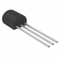
TO-226 (3)
4.30 mm × 4.30 mm
(1) For all available packages, see the orderable addendum at
the end of the datasheet.
4 Simplified Schematic
1
An IMPORTANT NOTICE at the end of this data sheet addresses availability, warranty, changes, use in safety-critical applications,
intellectual property matters and other important disclaimers. PRODUCTION DATA.
�LM285-1.2, LM385-1.2, LM385B-1.2
SLVS075J – APRIL 1989 – REVISED JANUARY 2015
www.ti.com
Table of Contents
1
2
3
4
5
6
7
8
Features ..................................................................
Applications ...........................................................
Description .............................................................
Simplified Schematic.............................................
Revision History.....................................................
Pin Configuration and Functions .........................
Specifications.........................................................
1
1
1
1
2
3
4
7.1
7.2
7.3
7.4
7.5
7.6
4
4
4
4
5
5
Absolute Maximum Ratings ......................................
ESD Ratings..............................................................
Recommended Operating Conditions.......................
Thermal Information ..................................................
Electrical Characteristics...........................................
Typical Characteristics ..............................................
Detailed Description .............................................. 7
8.1 Overview ................................................................... 7
8.2 Functional Block Diagram ......................................... 7
8.3 Feature Description................................................... 7
8.4 Device Functional Modes.......................................... 7
9
Application and Implementation .......................... 8
9.1 Application Information.............................................. 8
9.2 Typical Application ................................................... 8
9.3 System Examples ................................................... 10
10 Power Supply Recommendations ..................... 11
11 Layout................................................................... 11
11.1 Layout Guidelines ................................................. 11
11.2 Layout Example .................................................... 11
12 Device and Documentation Support ................. 12
12.1
12.2
12.3
12.4
Related Links ........................................................
Trademarks ...........................................................
Electrostatic Discharge Caution ............................
Glossary ................................................................
12
12
12
12
13 Mechanical, Packaging, and Orderable
Information ........................................................... 12
5 Revision History
Changes from Revision I (December 2005) to Revision J
Page
•
Added Applications, Device Information table, Pin Functions table, ESD Ratings table, Thermal Information table,
Typical Characteristics, Feature Description section, Device Functional Modes, Application and Implementation
section, Power Supply Recommendations section, Layout section, Device and Documentation Support section, and
Mechanical, Packaging, and Orderable Information section. ................................................................................................. 1
•
Deleted Ordering Information table. ....................................................................................................................................... 1
2
Submit Documentation Feedback
Copyright © 1989–2015, Texas Instruments Incorporated
Product Folder Links: LM285-1.2 LM385-1.2 LM385B-1.2
�LM285-1.2, LM385-1.2, LM385B-1.2
www.ti.com
SLVS075J – APRIL 1989 – REVISED JANUARY 2015
6 Pin Configuration and Functions
Pin Functions
PIN
NAME
TYPE
DESCRIPTION
LP
D, PS or PW
ANODE
1
4
I
Shunt Current/Voltage input
CATHODE
2
8
O
Common pin, normally connected to ground
NC
3
1, 2, 3, 5, 6, 7
—
No internal connection
Copyright © 1989–2015, Texas Instruments Incorporated
Submit Documentation Feedback
Product Folder Links: LM285-1.2 LM385-1.2 LM385B-1.2
3
�LM285-1.2, LM385-1.2, LM385B-1.2
SLVS075J – APRIL 1989 – REVISED JANUARY 2015
www.ti.com
7 Specifications
7.1 Absolute Maximum Ratings
over operating free-air temperature range (unless otherwise noted) (1)
MIN
IR
Reverse Current
IF
Forward Current
TJ
Operating virtual junction temperature
Tstg
Storage temeprature
(1)
MAX
–65
UNIT
30
mA
10
mA
150
°C
150
°C
Stresses beyond those listed under Absolute Maximum Ratings may cause permanent damage to the device. These are stress ratings
only, which do not imply functional operation of the device at these or any other conditions beyond those indicated under Recommended
Operating Conditions. Exposure to absolute-maximum-rated conditions for extended periods may affect device reliability.
7.2 ESD Ratings
VALUE
V(ESD)
(1)
(2)
Electrostatic discharge
Human body model (HBM), per ANSI/ESDA/JEDEC JS-001, all pins (1)
±2000
Charged device model (CDM), per JEDEC specification JESD22-C101,
all pins (2)
±1000
UNIT
V
JEDEC document JEP155 states that 500-V HBM allows safe manufacturing with a standard ESD control process.
JEDEC document JEP157 states that 250-V CDM allows safe manufacturing with a standard ESD control process.
7.3 Recommended Operating Conditions
over operating free-air temperature range (unless otherwise noted)
IZZ
Reference current
TA
Operating free-air temperature
MIN
MAX
0.01
20
–40
85
0
70
LM285-1.2
LM385-1.2, LM385B-1.2
UNIT
mA
°C
7.4 Thermal Information
LMx85-1.2
THERMAL METRIC (1)
RθJA
(1)
4
Junction-to-ambient thermal resistance
D
LP
PS
PW
8 PINS
3 PINS
8 PINS
8 PINS
97
140
95
149
UNIT
°C/W
For more information about traditional and new thermal metrics, see the IC Package Thermal Metrics application report, SPRA953.
Submit Documentation Feedback
Copyright © 1989–2015, Texas Instruments Incorporated
Product Folder Links: LM285-1.2 LM385-1.2 LM385B-1.2
�LM285-1.2, LM385-1.2, LM385B-1.2
www.ti.com
SLVS075J – APRIL 1989 – REVISED JANUARY 2015
7.5 Electrical Characteristics
over operating free-air temperature range (unless otherwise noted)
PARAMETER
TEST CONDITIONS
TA (1)
VZ
Reference voltage
IZ = I(min) to 20 mA (2)
25°C
αVZ
Average temperature
coefficient of reference
voltage (3)
IZ = I(min) to 20 mA (2)
Full
Range
LM285-1.2
Change in reference
voltage with current
ΔVZ
IZ = I(min) to 20 mA
ΔVZ/Δt
Long-term change in
reference voltage
IZ(min)
Minimum reference
current
ZZ
Reference impedance
IZ = 100 µA, f = 25 Hz
Vn
Broadband noise
voltage
IZ = 100 µA, f = 10 Hz to
10 kHz
IZ = 100 µA
MAX
MIN
TYP
MAX
MIN
TYP
MAX
1.223
1.235
1.247
1.21
1.235
1.26
1.223
1.235
1.247
±20
±20
1
1
1
1.5
1.5
1.5
25°C
12
20
20
Full
Range
30
30
30
25°C
Full
Range
±20
10
8
15
8
15
0.2
0.6
0.4
1
0.4
1
1.5
1.5
60
60
V
mV
ppm/k
hr
±20
8
Full
Range
25°C
±20
UNIT
ppm/°
C
±20
Full
Range
25°C
(1)
(2)
(3)
LM385B-1.2
TYP
25°C
IZ = I(min) to 1 mA (2)
LM385-1.2
MIN
µA
Ω
1.5
60
µV
Full range is −40°C to 85°C for the LM285-1.2 and 0°C to 70°C for the LM385-1.2 and LM385B-1.2.
I(min) = 10 μA for the LM285-1.2 and 15 μA for the LM385-1.2 and LM385B-1.2
The average temperature coefficient of reference voltage is defined as the total change in reference voltage divided by the specified
temperature range.
7.6 Typical Characteristics
Figure 1. Reverse Current vs Reverse Voltage
Copyright © 1989–2015, Texas Instruments Incorporated
Figure 2. Reference Voltage Change vs Reverse Current
Submit Documentation Feedback
Product Folder Links: LM285-1.2 LM385-1.2 LM385B-1.2
5
�LM285-1.2, LM385-1.2, LM385B-1.2
SLVS075J – APRIL 1989 – REVISED JANUARY 2015
www.ti.com
Typical Characteristics (continued)
Figure 3. Forward Voltage vs Forward Current
Figure 4. Reference Voltage vs Free-Air Temperature
Figure 5. Reference Impedance vs Reference Current
Figure 6. Noise Voltage vs Frequency
Figure 7. Output Noise Voltage vs Cutoff Frequency
6
Submit Documentation Feedback
Copyright © 1989–2015, Texas Instruments Incorporated
Product Folder Links: LM285-1.2 LM385-1.2 LM385B-1.2
�LM285-1.2, LM385-1.2, LM385B-1.2
www.ti.com
SLVS075J – APRIL 1989 – REVISED JANUARY 2015
8 Detailed Description
8.1 Overview
The LM285-1.2, LM385-1.2, and LM385-1.2 devices are micropower, two-terminal, band-gap voltage references
which operate over a 10-μA to 20-mA current range. On-chip trimming provides tight voltage tolerance. The
band-gap reference for these devices has low noise and long-term stability.
The design makes these devices exceptionally tolerant of capacitive loading and, thus, easier to use in most
reference applications. The wide dynamic operating temperature range accommodates varying current supplies,
with excellent regulation.
The extremely low power drain of this series makes them useful for micropower circuitry. These voltage
references can be used to make portable meters, regulators, or general-purpose analog circuitry, with battery life
approaching shelf life.
8.2 Functional Block Diagram
A.
Component values shown are nominal.
8.3 Feature Description
A band gap voltage reference controls high gain amplifier and shunt pass element to maintain a nearly constant
voltage between cathode and anode. Regulation occurs after a minimum current is provided to power the voltage
divider and amplifier. Internal frequency compensation provides a stable loop for all capacitor loads. Floating
shunt design is useful for both positive and negative regulation applications.
8.4 Device Functional Modes
LM285-1.2, LM385-1.2, and LM385-1.2 devices will operate in one mode, which is as a fixed voltage reference
that cannot be adjusted.
In order for a proper Reverse Voltage to be developed, current must be sourced into the cathode of LM285. The
minimum current needed for proper regulation is denoted in Electrical Characteristics as IZ,min.
Copyright © 1989–2015, Texas Instruments Incorporated
Submit Documentation Feedback
Product Folder Links: LM285-1.2 LM385-1.2 LM385B-1.2
7
�LM285-1.2, LM385-1.2, LM385B-1.2
SLVS075J – APRIL 1989 – REVISED JANUARY 2015
www.ti.com
9 Application and Implementation
NOTE
Information in the following applications sections is not part of the TI component
specification, and TI does not warrant its accuracy or completeness. TI’s customers are
responsible for determining suitability of components for their purposes. Customers should
validate and test their design implementation to confirm system functionality.
9.1 Application Information
The The LM285-1.2, LM385-1.2, and LM385-1.2 devices create a voltage reference for to be used for a variety of
applications including amplifiers, power supplies, and current-sensing circuits. The following application shows
how to use these devices to establish a voltage reference.
9.2 Typical Application
5V
36 k
1.2 V
LM385-1.2
Figure 8. Generating Reference Voltage with a Resistive Current Source
9.2.1 Design Requirements
The key design requirement when using this device as a voltage reference is to supply the LM385 with a
minimum Cathode Current (IZ), as indicated in Electrical Characteristics.
9.2.2 Detailed Design Procedure
In order to generate a constant and stable reference voltage, a current greater than IZ(MIN) must be sourced into
the cathode of this device. This can be accomplished using a current regulating device such as LM334 or a
simple resistor. For a resistor, its value should be equal to or greater than (Vsupply - Vreference) ÷ IZ(MIN) .
8
Submit Documentation Feedback
Copyright © 1989–2015, Texas Instruments Incorporated
Product Folder Links: LM285-1.2 LM385-1.2 LM385B-1.2
�LM285-1.2, LM385-1.2, LM385B-1.2
www.ti.com
SLVS075J – APRIL 1989 – REVISED JANUARY 2015
Typical Application (continued)
9.2.3 Application Curves
Figure 9. Transient Response
Copyright © 1989–2015, Texas Instruments Incorporated
Submit Documentation Feedback
Product Folder Links: LM285-1.2 LM385-1.2 LM385B-1.2
9
�LM285-1.2, LM385-1.2, LM385B-1.2
SLVS075J – APRIL 1989 – REVISED JANUARY 2015
www.ti.com
9.3 System Examples
9.3.1 Thermocouple Cold-Junction Compensator
Figure 10. Thermocouple Cold-Junction Compensator
9.3.2 Generating Reference Voltage with a Constant Current Source
Figure 11. Generating Reference Voltage with a Constant Current Source Device
10
Submit Documentation Feedback
Copyright © 1989–2015, Texas Instruments Incorporated
Product Folder Links: LM285-1.2 LM385-1.2 LM385B-1.2
�LM285-1.2, LM385-1.2, LM385B-1.2
www.ti.com
SLVS075J – APRIL 1989 – REVISED JANUARY 2015
10 Power Supply Recommendations
In order to not exceed the maximum cathode current, be sure that the supply voltage is current limited.
For applications shunting high currents (30 mA max), pay attention to the cathode and anode trace lengths,
adjusting the width of the traces to have the proper current density.
11 Layout
11.1 Layout Guidelines
Figure 12 shows an example of a PCB layout of LMx85x-1.2. Some key Vref niose considerations are:
• Connect a low-ESR, 0.1-μF (CL) ceramic bypass capacitor on the cathode pin node.
• Decouple other active devices in the system per the device specifications.
• Using a solid ground plane helps distribute heat and reduces electromagnetic interference (EMI) noise pickup.
• Place the external components as close to the device as possible. This configuration prevents parasitic errors
(such as the Seebeck effect) from occurring.
• Do not run sensitive analog traces in parallel with digital traces. Avoid crossing digital and analog traces if
possible and only make perpendicular crossings when absolutely necessary.
11.2 Layout Example
Rsup
NC 1
NC 2
NC 3
8
CATHODE
7
6
4
5
NC
NC
NC
ANODE
GND
Vsup
CL
GND
Figure 12. Layout Diagram
Copyright © 1989–2015, Texas Instruments Incorporated
Submit Documentation Feedback
Product Folder Links: LM285-1.2 LM385-1.2 LM385B-1.2
11
�LM285-1.2, LM385-1.2, LM385B-1.2
SLVS075J – APRIL 1989 – REVISED JANUARY 2015
www.ti.com
12 Device and Documentation Support
12.1 Related Links
The table below lists quick access links. Categories include technical documents, support and community
resources, tools and software, and quick access to sample or buy.
Table 1. Related Links
PARTS
PRODUCT FOLDER
SAMPLE & BUY
TECHNICAL
DOCUMENTS
TOOLS &
SOFTWARE
SUPPORT &
COMMUNITY
LM285-1.2
Click here
Click here
Click here
Click here
Click here
LM385-1.2
Click here
Click here
Click here
Click here
Click here
LM385B-1.2
Click here
Click here
Click here
Click here
Click here
12.2 Trademarks
All trademarks are the property of their respective owners.
12.3 Electrostatic Discharge Caution
These devices have limited built-in ESD protection. The leads should be shorted together or the device placed in conductive foam
during storage or handling to prevent electrostatic damage to the MOS gates.
12.4 Glossary
SLYZ022 — TI Glossary.
This glossary lists and explains terms, acronyms, and definitions.
13 Mechanical, Packaging, and Orderable Information
The following pages include mechanical, packaging, and orderable information. This information is the most
current data available for the designated devices. This data is subject to change without notice and revision of
this document. For browser-based versions of this data sheet, refer to the left-hand navigation.
12
Submit Documentation Feedback
Copyright © 1989–2015, Texas Instruments Incorporated
Product Folder Links: LM285-1.2 LM385-1.2 LM385B-1.2
�PACKAGE OPTION ADDENDUM
www.ti.com
26-Feb-2022
PACKAGING INFORMATION
Orderable Device
Status
(1)
Package Type Package Pins Package
Drawing
Qty
Eco Plan
(2)
Lead finish/
Ball material
MSL Peak Temp
Op Temp (°C)
Device Marking
(3)
(4/5)
(6)
LM285D-1-2
ACTIVE
SOIC
D
8
75
RoHS & Green
NIPDAU
Level-1-260C-UNLIM
-40 to 85
285-12
LM285DG4-1-2
ACTIVE
SOIC
D
8
75
RoHS & Green
NIPDAU
Level-1-260C-UNLIM
-40 to 85
285-12
LM285DR-1-2
ACTIVE
SOIC
D
8
2500
RoHS & Green
NIPDAU
Level-1-260C-UNLIM
-40 to 85
285-12
LM285DRE4-1-2
ACTIVE
SOIC
D
8
2500
RoHS & Green
NIPDAU
Level-1-260C-UNLIM
-40 to 85
285-12
LM285DRG4-1-2
ACTIVE
SOIC
D
8
2500
RoHS & Green
NIPDAU
Level-1-260C-UNLIM
-40 to 85
285-12
LM285LP-1-2
ACTIVE
TO-92
LP
3
1000
RoHS & Green
SN
N / A for Pkg Type
-40 to 85
285-12
LM285LPE3-1-2
ACTIVE
TO-92
LP
3
1000
RoHS & Green
SN
N / A for Pkg Type
-40 to 85
285-12
LM285LPRE3-1-2
ACTIVE
TO-92
LP
3
2000
RoHS & Green
SN
N / A for Pkg Type
-40 to 85
285-12
LM385BD-1-2
ACTIVE
SOIC
D
8
75
RoHS & Green
NIPDAU
Level-1-260C-UNLIM
0 to 70
385B12
LM385BDG4-1-2
ACTIVE
SOIC
D
8
75
RoHS & Green
NIPDAU
Level-1-260C-UNLIM
0 to 70
385B12
LM385BDR-1-2
ACTIVE
SOIC
D
8
2500
RoHS & Green
NIPDAU
Level-1-260C-UNLIM
0 to 70
385B12
LM385BDRG4-1-2
ACTIVE
SOIC
D
8
2500
RoHS & Green
NIPDAU
Level-1-260C-UNLIM
0 to 70
385B12
LM385BLP-1-2
ACTIVE
TO-92
LP
3
1000
RoHS & Green
SN
N / A for Pkg Type
0 to 70
385B12
LM385BLPE3-1-2
ACTIVE
TO-92
LP
3
1000
RoHS & Green
SN
N / A for Pkg Type
0 to 70
385B12
LM385BLPR-1-2
ACTIVE
TO-92
LP
3
2000
RoHS & Green
SN
N / A for Pkg Type
0 to 70
385B12
LM385BLPRE3-1-2
ACTIVE
TO-92
LP
3
2000
RoHS & Green
SN
N / A for Pkg Type
0 to 70
385B12
LM385BPW-1-2
ACTIVE
TSSOP
PW
8
150
RoHS & Green
NIPDAU
Level-1-260C-UNLIM
0 to 70
385B12
LM385BPWR-1-2
ACTIVE
TSSOP
PW
8
2000
RoHS & Green
NIPDAU
Level-1-260C-UNLIM
0 to 70
385B12
LM385D-1-2
ACTIVE
SOIC
D
8
75
RoHS & Green
NIPDAU
Level-1-260C-UNLIM
0 to 70
385-12
LM385DG4-1-2
ACTIVE
SOIC
D
8
75
RoHS & Green
NIPDAU
Level-1-260C-UNLIM
0 to 70
385-12
Addendum-Page 1
Samples
�PACKAGE OPTION ADDENDUM
www.ti.com
26-Feb-2022
Orderable Device
Status
(1)
Package Type Package Pins Package
Drawing
Qty
Eco Plan
(2)
Lead finish/
Ball material
MSL Peak Temp
Op Temp (°C)
Device Marking
(3)
(4/5)
(6)
LM385DR-1-2
ACTIVE
SOIC
D
8
2500
RoHS & Green
NIPDAU
Level-1-260C-UNLIM
0 to 70
385-12
LM385LP-1-2
ACTIVE
TO-92
LP
3
1000
RoHS & Green
SN
N / A for Pkg Type
0 to 70
385-12
LM385LPR-1-2
ACTIVE
TO-92
LP
3
2000
RoHS & Green
SN
N / A for Pkg Type
0 to 70
385-12
LM385LPRE3-1-2
ACTIVE
TO-92
LP
3
2000
RoHS & Green
SN
N / A for Pkg Type
0 to 70
385-12
LM385PW-1-2
ACTIVE
TSSOP
PW
8
150
RoHS & Green
NIPDAU
Level-1-260C-UNLIM
0 to 70
385-12
LM385PWE4-1-2
ACTIVE
TSSOP
PW
8
150
RoHS & Green
NIPDAU
Level-1-260C-UNLIM
0 to 70
385-12
LM385PWR-1-2
ACTIVE
TSSOP
PW
8
2000
RoHS & Green
NIPDAU
Level-1-260C-UNLIM
0 to 70
385-12
LM385PWRE4-1-2
ACTIVE
TSSOP
PW
8
2000
RoHS & Green
NIPDAU
Level-1-260C-UNLIM
0 to 70
385-12
(1)
The marketing status values are defined as follows:
ACTIVE: Product device recommended for new designs.
LIFEBUY: TI has announced that the device will be discontinued, and a lifetime-buy period is in effect.
NRND: Not recommended for new designs. Device is in production to support existing customers, but TI does not recommend using this part in a new design.
PREVIEW: Device has been announced but is not in production. Samples may or may not be available.
OBSOLETE: TI has discontinued the production of the device.
(2)
RoHS: TI defines "RoHS" to mean semiconductor products that are compliant with the current EU RoHS requirements for all 10 RoHS substances, including the requirement that RoHS substance
do not exceed 0.1% by weight in homogeneous materials. Where designed to be soldered at high temperatures, "RoHS" products are suitable for use in specified lead-free processes. TI may
reference these types of products as "Pb-Free".
RoHS Exempt: TI defines "RoHS Exempt" to mean products that contain lead but are compliant with EU RoHS pursuant to a specific EU RoHS exemption.
Green: TI defines "Green" to mean the content of Chlorine (Cl) and Bromine (Br) based flame retardants meet JS709B low halogen requirements of