Product
Folder
Order
Now
Support &
Community
Tools &
Software
Technical
Documents
LM139, LM239, LM339, LM139A
LM239A, LM339A, LM2901, LM2901AV, LM2901V
ZHCSJ12U – OCTOBER 1979 – REVISED NOVEMBER 2018
LM339、
、LM239、
、LM139、
、LM2901 四路差分比较器
1 特性
•
1
•
•
•
•
•
•
•
•
•
3 说明
宽电源范围
– 单电源:2V 至 36 V
(对于非 V 后缀器件进行了 30V 测试,
对于 V 后缀器件进行了 32V 测试)
– 双电源:±1V 至 ±18V
(对于非 V 后缀器件进行了 ±15V 测试,
对于 V 后缀器件进行了 ±16V 测试)
独立于电源电压的低电源电流
消耗:0.8mA(典型值)
低输入偏置电流:25nA(典型值)
低输入失调电流:3nA(典型值)(LM139)
低输入失调电压:2mV(典型值)
共模输入电压范围
包括接地
差分输入电压范围等于最大额定电源电压:±36V
低输出饱和电压
输出与 TTL、MOS 和 CMOS 兼容
对于符合 MIL-PRF-38535 标准的产品,
所有参数均经过测试,除非另外注明。对于所有其
他产品,生产流程不一定包含对所有参数的测试。
2 应用
•
•
•
•
•
•
工业
汽车应用
– 信息娱乐系统和仪表组
– 车身控制模块
电源监控
振荡器
峰值检测器
逻辑电压转换
LMx39x 和 LM2901x 器件包含四个独立的电压比较
器,这些比较器可在宽电压范围内由单电源供电。这些
器件也可以由双电源供电,只要两个电源之间的电压差
处于 2V 至 36V 的范围之内且 VCC 比输入共模电压至
少高 +1.5V 以上即可。漏极电流不受电源电压的影
响。可将输出连接到其它集电极开路输出,以实现有线
AND 关联。
LM139 和 LM139A 器件在 –55°C 至 +125°C 的完整
军用温度范围内运行。LM239 和 LM239A 器件的额定
工作温度范围是 –25°C 至 +85°C。LM339 和 LM339A
器件的额定工作温度范围是 –0°C 至 70°C。LM2901、
LM2901AV 和 LM2901V 器件的额定工作温度范围是
–40°C 至 125°C。
器件信息(1)
器件型号
封装
封装尺寸(标称值)
CDIP (14)
21.30mm × 7.60mm
LCCC (20)
8.90mm × 8.90mm
CFP (14)
9.20mm × 6.29mm
LM139x、
LM239x、
LM339x、
LM2901x
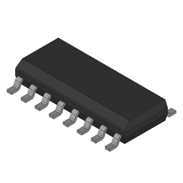
SOIC (14)
8.70mm × 3.90mm
LM239、
LM339x、
LM2901
PDIP (14)
19.30mm × 6.40mm
LM139x
LM239、LM2901 TSSOP (14)
5.00mm × 4.40mm
LM339x、
LM2901
SO (14)
10.20mm × 5.30mm
LM339x
SSOP (14)
6.50mm × 5.30mm
(1) 如需了解所有可用封装,请参阅数据表末尾的可订购产品附
录。
简化原理图
IN+
OUT
IN−
1
本文档旨在为方便起见,提供有关 TI 产品中文版本的信息,以确认产品的概要。 有关适用的官方英文版本的最新信息,请访问 www.ti.com,其内容始终优先。 TI 不保证翻译的准确
性和有效性。 在实际设计之前,请务必参考最新版本的英文版本。
English Data Sheet: SLCS006
�LM139, LM239, LM339, LM139A
LM239A, LM339A, LM2901, LM2901AV, LM2901V
ZHCSJ12U – OCTOBER 1979 – REVISED NOVEMBER 2018
www.ti.com.cn
目录
1
2
3
4
5
6
7
特性 ..........................................................................
应用 ..........................................................................
说明 ..........................................................................
修订历史记录 ...........................................................
Device Comparison Table.....................................
Pin Configuration and Functions .........................
Specifications.........................................................
7.1
7.2
7.3
7.4
7.5
7.6
7.7
7.8
1
1
1
2
3
4
5
Absolute Maximum Ratings ...................................... 5
ESD Ratings.............................................................. 5
Recommended Operating Conditions....................... 5
Thermal Information (14-Pin Packages) ................... 6
Thermal Information (20-Pin Packages) ................... 6
Electrical Characteristics for LM139 and LM139A.... 7
Electrical Characteristics for LMx39 and LMx39A .... 7
Electrical Characteristics for LM2901, LM2901V and
LM2901AV ................................................................. 8
7.9 Switching Characteristics for LM2901....................... 9
7.10 Switching Characteristics for LM139 and LM139A . 9
7.11 Switching Characteristics for LMx39 and LMx39A . 9
7.12 Typical Characteristics .......................................... 10
8
Detailed Description ............................................ 11
8.1
8.2
8.3
8.4
9
Overview .................................................................
Functional Block Diagram .......................................
Feature Description.................................................
Device Functional Modes........................................
11
11
11
11
Application and Implementation ........................ 12
9.1 Application Information............................................ 12
9.2 Typical Application ................................................. 12
10 Power Supply Recommendations ..................... 14
11 Layout................................................................... 14
11.1 Layout Guidelines ................................................. 14
11.2 Layout Example .................................................... 14
12 器件和文档支持 ..................................................... 15
12.1
12.2
12.3
12.4
12.5
12.6
相关链接................................................................
接收文档更新通知 .................................................
社区资源................................................................
商标 .......................................................................
静电放电警告.........................................................
术语表 ...................................................................
15
15
15
15
15
15
13 机械、封装和可订购信息 ....................................... 15
4 修订历史记录
注:之前版本的页码可能与当前版本有所不同。
Changes from Revision T (June 2015) to Revision U
Page
•
已更改 在说明 部分中将 LM239x 温度范围从 125°C 更改成了 85°C ..................................................................................... 1
•
已更改 更改了数据表标题 ...................................................................................................................................................... 1
•
Changed LM293AD to LM239AD in Device Comparison Table............................................................................................. 3
•
Changed 'I' to dash in GND and VCC in I/O column of the Pin Functions table.................................................................... 4
•
Added Input Current and related footnote in Absolute Maximum Ratings ............................................................................. 5
•
Changed layout of Recommended Operating Conditions temperatures to separate rows .................................................... 5
•
Changed values in the Thermal Information table to align with JEDEC standards................................................................ 6
•
Added LM2901V and LMV2901AV to LM2901 Elect Char Table title to make more clear which devices are covered. ....... 8
•
Changed "Dual" to "Quad" and removed "Absolute Maximum" wording and mention of Q100 in Overview section text. .. 11
•
Changed and corrected text in Feature Description section ................................................................................................ 11
•
Changed Example Values in Typical Application Design Parameters table ....................................................................... 12
•
已添加 添加了接收文档更新通知 部分 .................................................................................................................................. 15
Changes from Revision S (August 2012) to Revision T
Page
•
删除了订购信息 表。 .............................................................................................................................................................. 1
•
在特性 列表中添加了“军用免责声明”。................................................................................................................................... 1
•
添加了 应用、器件信息 表、引脚配置和功能 部分、ESD 额定值 表、热性能信息 表、特性 说明 部分、器件功能模
式、应用和实施 部分、电源建议 部分、布局 部分、器件和文档支持 部分以及机械、封装和可订购信息 部分。无规格
变化。 ..................................................................................................................................................................................... 1
2
Copyright © 1979–2018, Texas Instruments Incorporated
�LM139, LM239, LM339, LM139A
LM239A, LM339A, LM2901, LM2901AV, LM2901V
www.ti.com.cn
ZHCSJ12U – OCTOBER 1979 – REVISED NOVEMBER 2018
5 Device Comparison Table
PART NUMBER
PACKAGE
BODY SIZE (NOM)
LM139J, LM139AJ
CDIP (14)
21.30 mm × 7.60 mm
LM139FK, LM139AFK
LCCC (20)
8.90 mm × 8.90 mm
LM139W, LM139AW
CFP (14)
9.20 mm × 6.29 mm
LM139D, LM139AD, LM239D, LM239AD, LM339D,
LM339AD, LM2901D
SOIC (14)
8.70 mm × 3.90 mm
LM239N, LM339N, LM339AN, LM2901N
PDIP (14)
19.30 mm × 6.40 mm
LM239PW, LM2901PW
TSSOP (14)
5.00 mm × 4.40 mm
LM339NS, LM339ANS, LM2901NS
SOP (14)
10.20 mm × 5.30 mm
LM339DB, LM339ADB
SSOP (14)
6.50 mm × 5.30 mm
OTHER QUALIFIED VERSIONS OF LM139-SP, LM239A, LM2901, LM2901AV, LM2901V:
•
•
•
Automotive Q100: LM239A-Q1, LM2901-Q1, LM2901AV-Q1, LM2901V-Q1
Enhanced Product: LM239A-EP
Space: LM139-SP
Copyright © 1979–2018, Texas Instruments Incorporated
3
�LM139, LM239, LM339, LM139A
LM239A, LM339A, LM2901, LM2901AV, LM2901V
ZHCSJ12U – OCTOBER 1979 – REVISED NOVEMBER 2018
www.ti.com.cn
6 Pin Configuration and Functions
D, DB, N, NS, PW, J, or W Package
SOIC, SSOP, PDIP, SO, TSSOP, CDIP, or CFP
Top View
14
2
13
3
12
4
11
5
10
6
9
7
8
2OUT
1OUT
NC
3OUT
4OUT
1
OUT3
OUT4
GND
4IN+
4IN−
3IN+
3IN−
3
VC C
NC
2IN−
NC
2IN+
4
2 1 20 19
18
17
16
5
6
15
7
8
14
9 10 11 12 13
GND
NC
4IN+
NC
4IN−
1IN−
1IN+
NC
3IN−
3IN+
1OUT
2OUT
VC C
2IN−
2IN+
1IN−
1IN+
FK Package
20-Pin LCCC(1)
Top View
(1)
NC = no internal connection.
Pin Functions
PIN
D, J, W, B,
PW, DB, N, NS
FK
1IN+
7
10
1IN–
6
1OUT
1
2IN+
NAME
I/O (1)
DESCRIPTION
I
Positive input pin of the comparator 1
9
I
Negative input pin of the comparator 1
2
O
Output pin of the comparator 1
5
8
I
Positive input pin of the comparator 2
2IN–
4
6
I
Negative input pin of the comparator 2
2OUT
2
3
O
Output pin of the comparator 2
3IN+
9
13
I
Positive input pin of the comparator 3
3IN–
8
12
I
Negative input pin of the comparator 3
3OUT
14
20
O
Output pin of the comparator 3
4IN+
11
16
I
Positive input pin of the comparator 4
4IN–
10
14
I
Negative input pin of the comparator 4
4OUT
13
19
O
Output pin of the comparator 4
GND
12
18
—
Ground
VCC
3
4
—
Supply pin
—
No connect (no internal connection)
1
5
NC
—
7
11
15
17
(1)
4
I = Input, O = Output
Copyright © 1979–2018, Texas Instruments Incorporated
�LM139, LM239, LM339, LM139A
LM239A, LM339A, LM2901, LM2901AV, LM2901V
www.ti.com.cn
ZHCSJ12U – OCTOBER 1979 – REVISED NOVEMBER 2018
7 Specifications
7.1 Absolute Maximum Ratings
over operating free-air temperature range (unless otherwise noted) (1)
MIN
MAX
UNIT
36
V
±36
V
Supply voltage (2)
VCC
(3)
VID
Differential input voltage
VI
Input voltage range (either input)
IK
–0.3
36
V
Input current (4)
–50
mA
VO
Output voltage
36
V
IO
Output current
20
mA
Duration of output short circuit to ground (5)
TJ
Operating virtual-junction temperature
Tstg
(1)
(2)
(3)
(4)
(5)
Unlimited
150
°C
Case temperature for 60 s
FK package
260
°C
Lead temperature 1.6 mm (1/16 in) from case for 60 s
J package
300
°C
150
°C
Storage temperature
–65
Stresses beyond those listed under Absolute Maximum Ratings may cause permanent damage to the device. These are stress ratings
only, and functional operation of the device at these or any other conditions beyond those indicated under Recommended Operating
Conditions is not implied. Exposure to absolute-maximum-rated conditions for extended periods may affect device reliability.
All voltage values, except differential voltages, are with respect to network ground.
Differential voltages are at xIN+ with respect to xIN–.
Input current flows through parasitic diode to ground and will turn on parasitic transistors that will increase ICC and may cause output to
be incorrect. Normal operation resumes when input is removed.
Short circuits from outputs to VCC can cause excessive heating and eventual destruction.
7.2 ESD Ratings
VALUE
V(ESD)
(1)
(2)
Electrostatic discharge
Human body model (HBM), per ANSI/ESDA/JEDEC JS-001
(1)
±500
Charged-device model (CDM), per JEDEC specification JESD22-C101 (2)
±750
UNIT
V
JEDEC document JEP155 states that 500-V HBM allows safe manufacturing with a standard ESD control process.
JEDEC document JEP157 states that 250-V CDM allows safe manufacturing with a standard ESD control process.
7.3 Recommended Operating Conditions
over operating free-air temperature range (unless otherwise noted)
VCC
TJ
Supply voltage
Junction temperature
Non-V devices
V devices
MIN
MAX
UNIT
2
30
V
V
2
32
LM139x
–55
125
LM239x
–25
85
LM339x
–0
70
LM2901x
–40
125
Copyright © 1979–2018, Texas Instruments Incorporated
°C
5
�LM139, LM239, LM339, LM139A
LM239A, LM339A, LM2901, LM2901AV, LM2901V
ZHCSJ12U – OCTOBER 1979 – REVISED NOVEMBER 2018
www.ti.com.cn
7.4 Thermal Information (14-Pin Packages)
LMx39, LM2901x
THERMAL METRIC (1)
D
(SOIC)
DB
(SSOP)
N
(PDIP)
NS
(SO)
PW
(TSSOP)
J
(CDIP)
W
(CFP)
UNIT
120
89.5
156.2
°C/W
RθJA
Junction-to-ambient thermal resistance
98.8
111.8
79
96.2
RθJC(top)
Junction-to-case (top) thermal resistance
64.3
63.6
73.4
56.1
59
46.1
86.7
°C/W
RθJB
Junction-to-board thermal resistance
59.7
60.5
58.7
56.9
68.8
78.7
154.6
°C/W
ψJT
Junction-to-top characterization parameter
25.7
26.2
48.3
24.8
9.9
3
56.5
°C/W
ψJB
Junction-to-board characterization
parameter
59.3
59.8
58.5
56.4
68.2
71.8
133.5
°C/W
RθJC(bot)
Junction-to-case (bottom) thermal
resistance
—
—
—
—
—
24.2
14.3
°C/W
(1)
For more information about traditional and new thermal metrics, see the Semiconductor and IC Package Thermal Metrics application
report.
7.5 Thermal Information (20-Pin Packages)
THERMAL METRIC (1)
LM139x
FK (LCCC)
UNIT
RθJA
Junction-to-ambient thermal resistance
82.5
°C/W
RθJC(top)
Junction-to-case (top) thermal resistance
60.7
°C/W
RθJB
Junction-to-board thermal resistance
59.4
°C/W
ψJT
Junction-to-top characterization parameter
53
°C/W
ψJB
Junction-to-board characterization parameter
58.4
°C/W
RθJC(bot)
Junction-to-case (bottom) thermal resistance
9.7
°C/W
(1)
6
For more information about traditional and new thermal metrics, see the Semiconductor and IC Package Thermal Metrics application
report.
Copyright © 1979–2018, Texas Instruments Incorporated
�LM139, LM239, LM339, LM139A
LM239A, LM339A, LM2901, LM2901AV, LM2901V
www.ti.com.cn
ZHCSJ12U – OCTOBER 1979 – REVISED NOVEMBER 2018
7.6 Electrical Characteristics for LM139 and LM139A
at specified free-air temperature, VCC = 5 V (unless otherwise noted)
PARAMETER
TEST CONDITIONS (1)
VIO
Input offset voltage
VCC = 5 V to 30 V,
VIC = VICR min,
VO = 1.4 V
IIO
Input offset current
VO = 1.4 V
IIB
Input bias current
VO = 1.4 V
VICR
Common-mode inputvoltage range (3)
25°C
TYP MAX
2
3
Full range
AVD
IOH
High-level output current
VID = 1 V
25
–300
–300
0 to
VCC – 1.5
0 to
–2
0 to
–2
VCC
25°C
0.1
VOH = 30 V
Full range
IOL
Low-level output current
VID = –1 V,
VOL = 1.5 V
25°C
ICC
Supply current
(four comparators)
VO = 2.5 V,
No load
25°C
50
150
200
V/mV
0.1
nA
150
mV
700
16
6
0.8
μA
400
700
6
nA
1
400
Full range
nA
V
1
25°C
IOL = 4 mA
25
–25 –100
VOH = 5 V
VID = –1 V,
3
0 to
VCC – 1.5
VCC
mV
4
–25 –100
200
Low-level output voltage
2
100
25°C
VOL
1
100
Full range
UNIT
TYP MAX
9
25°C
25°C
MIN
5
Full range
25°C
VCC+ = ±7.5 V,
VO = –5 V to 5 V
(3)
MIN
LM139A
Full range
Large-signal differentialvoltage amplification
(1)
(2)
LM139
TA (2)
2
16
mA
0.8
2
mA
All characteristics are measured with zero common-mode input voltage, unless otherwise specified.
Full range (MIN to MAX) for LM139 and LM139A is –55°C to +125°C. All characteristics are measured with zero common-mode input
voltage, unless otherwise specified.
The voltage at either input or common-mode must not be allowed to go negative by more than 0.3 V. The upper end of the commonmode voltage range is VCC+ – 1.5 V; however, one input can exceed VCC, and the comparator will provide a proper output state as long
as the other input remains in the common-mode range. Either or both inputs can go to 30 V without damage.
7.7 Electrical Characteristics for LMx39 and LMx39A
at specified free-air temperature, VCC = 5 V (unless otherwise noted)
PARAMETER
TEST CONDITIONS (1)
LM239
LM339
TA (2)
MIN
VIO
Input offset voltage
VCC = 5 V to 30 V,
VIC = VICR min,
VO = 1.4 V
IIO
Input offset current
VO = 1.4 V
IIB
Input bias current
VO = 1.4 V
VICR
Common-mode inputvoltage range (3)
AVD
(1)
(2)
(3)
Large-signal differentialvoltage amplification
25°C
TYP MAX
2
Full range
25°C
5
25°C
25°C
5
1
50
5
50
150
–25 –250
–25 –250
–400
–400
0 to
VCC – 1.5
0 to
–2
0 to
–2
50
3
4
0 to
VCC – 1.5
VCC
UNIT
TYP MAX
150
Full range
Full range
MIN
9
Full range
25°C
VCC = 15 V,
VO = 1.4 V to 11.4 V,
RL ≥ 15 kΩ to VCC
LM239A
LM339A
VCC
200
50
mV
nA
nA
V
200
V/mV
All characteristics are measured with zero common-mode input voltage, unless otherwise specified.
Full range (MIN to MAX) for LM239/LM239A is –25°C to +85°C, and for LM339/LM339A is 0°C to 70°C. All characteristics are measured
with zero common-mode input voltage, unless otherwise specified.
The voltage at either input or common-mode must not be allowed to go negative by more than 0.3 V. The upper end of the commonmode voltage range is VCC+ – 1.5 V; however, one input can exceed VCC, and the comparator will provide a proper output state as long
as the other input remains in the common-mode range. Either or both inputs can go to 30 V without damage.
Copyright © 1979–2018, Texas Instruments Incorporated
7
�LM139, LM239, LM339, LM139A
LM239A, LM339A, LM2901, LM2901AV, LM2901V
ZHCSJ12U – OCTOBER 1979 – REVISED NOVEMBER 2018
www.ti.com.cn
Electrical Characteristics for LMx39 and LMx39A (continued)
at specified free-air temperature, VCC = 5 V (unless otherwise noted)
PARAMETER
TEST CONDITIONS (1)
TA (2)
LM239
LM339
MIN
VOH = 5 V
25°C
VOH = 30 V
Full range
IOH
High-level output current
VID = 1 V
VOL
Low-level output voltage
VID = –1 V,
IOL = 4 mA
IOL
Low-level output current
VID = –1 V,
VOL = 1.5 V
25°C
ICC
Supply current
(four comparators)
VO = 2.5 V,
No load
25°C
LM239A
LM339A
TYP MAX
0.1
MIN
UNIT
TYP MAX
50
0.1
1
25°C
150
Full range
400
150
700
6
nA
1
μA
400
700
16
0.8
50
6
16
2
mV
mA
0.8
2
mA
7.8 Electrical Characteristics for LM2901, LM2901V and LM2901AV
at specified free-air temperature, VCC = 5 V (unless otherwise noted)
TEST CONDITIONS (1)
PARAMETER
VIO
Input offset voltage
VIC = VICR min,
VO = 1.4 V,
VCC = 5 V to MAX (3)
IIO
Input offset current
VO = 1.4 V
IIB
Input bias current
VO = 1.4 V
VICR
Common-mode inputvoltage range (4)
Non-A devices
A-suffix devices
2
Full range
25°C
2
5
50
IOH
High-level output current
VID = 1 V
VOL
Low-level output voltage
VID = –1 V,
IOL = 4 mA
VOH = 5 V
VOH = VCC MAX (3)
Non-V devices
V-suffix devices
25°C
200
–25
Low-level output current
VID = –1 V,
VOL = 1.5 V
ICC
Supply current
(four comparators)
VO = 2.5 V,
No load
VCC = 5 V
VCC = MAX (3)
VCC
25
25°C
nA
nA
V
0 to
–2
100
0.1
25°C
25°C
IOL
0 to
VCC – 1.5
25°C
Full range
–250
–500
Full range
All devices
mV
4
25°C
Full range
UNIT
7
1
Full range
25°C
MAX
15
Full range
VCC = 15 V, VO = 1.4 V to 11.4 V,
RL ≥ 15 kΩ to VCC
8
25°C
TYP
Full range
Large-signal differentialvoltage amplification
(3)
(4)
MIN
25°C
AVD
(1)
(2)
LM2901
TA (2)
V/mV
50
nA
1
μA
150
500
150
400
mV
700
6
16
mA
0.8
2
1
2.5
mA
All characteristics are measured with zero common-mode input voltage, unless otherwise specified.
Full range (MIN to MAX) for LM2901 is –40°C to +125°C. All characteristics are measured with zero common-mode input voltage,
unless otherwise specified.
VCC MAX = 30 V for non-V devices, and 32 V for V-suffix devices
The voltage at either input or common-mode must not be allowed to go negative by more than 0.3 V. The upper end of the commonmode voltage range is VCC+ – 1.5 V; however, one input can exceed VCC, and the comparator will provide a proper output state as long
as the other input remains in the common-mode range. Either or both inputs can go to VCC MAX without damage.
Copyright © 1979–2018, Texas Instruments Incorporated
�LM139, LM239, LM339, LM139A
LM239A, LM339A, LM2901, LM2901AV, LM2901V
www.ti.com.cn
ZHCSJ12U – OCTOBER 1979 – REVISED NOVEMBER 2018
7.9 Switching Characteristics for LM2901
VCC = 5 V, TA = 25°C
PARAMETER
Response time
(1)
(2)
TEST CONDITIONS
RL connected to 5 V through 5.1 kΩ,
CL = 15 pF (1) (2)
LM2901
TYP
100-mV input step with 5-mV overdrive
1.3
TTL-level input step
0.3
UNIT
μs
CL includes probe and jig capacitance.
The response time specified is the interval between the input step function and the instant when the output crosses 1.4 V.
7.10 Switching Characteristics for LM139 and LM139A
VCC = 5 V, TA = 25°C
PARAMETER
TEST CONDITIONS
LM139
LM139A
UNIT
TYP
Response time
(1)
(2)
RL connected to 5 V through 5.1 kΩ,
CL = 15 pF (1) (2)
100-mV input step with 5-mV overdrive
1.3
TTL-level input step
0.3
μs
CL includes probe and jig capacitance.
The response time specified is the interval between the input step function and the instant when the output crosses 1.4 V.
7.11 Switching Characteristics for LMx39 and LMx39A
VCC = 5 V, TA = 25°C
PARAMETER
TEST CONDITIONS
LM239
LM239A
LM339
LM339A
UNIT
TYP
Response time
(1)
(2)
RL connected to 5 V through 5.1 kΩ,
CL = 15 pF (1) (2)
100-mV input step with 5-mV overdrive
1.3
TTL-level input step
0.3
μs
CL includes probe and jig capacitance.
The response time specified is the interval between the input step function and the instant when the output crosses 1.4 V.
Copyright © 1979–2018, Texas Instruments Incorporated
9
�LM139, LM239, LM339, LM139A
LM239A, LM339A, LM2901, LM2901AV, LM2901V
ZHCSJ12U – OCTOBER 1979 – REVISED NOVEMBER 2018
www.ti.com.cn
7.12 Typical Characteristics
80
1.8
1.6
IIN – Input Bias Current – nA
ICC – Supply Current – mA
70
TA = –55°C
1.4
TA = 25°C
TA = 0°C
1.2
1
TA = 70°C
0.8
TA = 125°C
0.6
0.4
TA = –55°C
60
TA = 0°C
50
TA = 25°C
40
TA = 70°C
30
TA = 125°C
20
10
0.2
0
0
0
5
10
15
20
25
30
35
0
5
10
15
20
25
30
35
VCC – Supply Voltage – V
VCC – Supply Voltage – V
Figure 1. Supply Current vs Supply Voltage
Figure 2. Input Bias Current vs Supply Voltage
6
10
Overdrive = 5 mV
1
VO – Output Voltage – V
VO – Saturation Voltage – V
5
TA = 125°C
TA = 25°C
0.1
TA = –55°C
0.01
4
Overdrive = 20 mV
3
Overdrive = 100 mV
2
1
0
0.001
0.01
0.1
1
10
-1
-0.3
100
0
0.25 0.5 0.75
1
1.25 1.5 1.75
2
2.25
t – Time – µs
IO – Output Sink Current – mA
Figure 4. Response Time for Various Overdrives
Negative Transition
Figure 3. Output Saturation Voltage
6
VO – Output Voltage – V
5
Overdrive = 5 mV
4
Overdrive = 20 mV
3
Overdrive = 100 mV
2
1
0
-1
-0.3
0
0.25 0.5 0.75
1
1.25 1.5 1.75
2
2.25
t – Time – µs
Figure 5. Response Time for Various Overdrives
Positive Transition
10
Copyright © 1979–2018, Texas Instruments Incorporated
�LM139, LM239, LM339, LM139A
LM239A, LM339A, LM2901, LM2901AV, LM2901V
www.ti.com.cn
ZHCSJ12U – OCTOBER 1979 – REVISED NOVEMBER 2018
8 Detailed Description
8.1 Overview
The LMx39 and LM2901x are quad comparators with the ability to operate up to an absolute maximum of 36 V
on the supply pin. This standard device has proven ubiquity and versatility across a wide range of applications.
This is due to very wide supply voltages range (2 V up to 32 V), low Iq, and fast response of the device.
The open-drain output allows the user to configure the output logic low voltage (VOL) and allows the comparator
to be used in AND functionality.
8.2 Functional Block Diagram
VCC
80-µA
Current Regulator
60 µA
10 µA
IN+
10 µA
80 µA
COMPONENT COUNT
OUT
Epi-FET
Diodes
Resistors
Transistors
1
2
2
30
IN−
GND
Figure 6. Schematic (Each Comparator)
8.3 Feature Description
The comparator consists of a PNP Darlington pair input, allowing the device to operate with very high gain and
fast response with minimal input bias current. The input Darlington pair creates a limit on the input commonmode voltage capability, allowing the comparator to accurately function from ground to (VCC – 1.5 V) differential
input. Allow for (VCC – 2 V) at cold temperature.
The output consists of an open-collector NPN (pulldown or low-side) transistor. The output NPN sinks current
when the negative input voltage is higher than the positive input voltage and the offset voltage. The VOL is
resistive and scales with the output current. See the Specifications section for VOL values with respect to the
output current.
8.4 Device Functional Modes
8.4.1 Voltage Comparison
The comparator operates solely as a voltage comparator, comparing the differential voltage between the positive
and negative pins and outputting a logic low or high impedance (logic high with pullup) based on the input
differential polarity.
Copyright © 1979–2018, Texas Instruments Incorporated
11
�LM139, LM239, LM339, LM139A
LM239A, LM339A, LM2901, LM2901AV, LM2901V
ZHCSJ12U – OCTOBER 1979 – REVISED NOVEMBER 2018
www.ti.com.cn
9 Application and Implementation
NOTE
Information in the following applications sections is not part of the TI component
specification, and TI does not warrant its accuracy or completeness. TI’s customers are
responsible for determining suitability of components for their purposes. Validate and test
the design implementation to confirm system functionality.
9.1 Application Information
Typically, a comparator compares either a single signal to a reference, or to two differnt signals. Many users take
advantage of the open-drain output to drive the comparison logic output to a logic voltage level to an MCU or
logic device. The wide supply range and high voltage capability makes LMx39 or LM2901x optimal for level
shifting to a higher or lower voltage.
9.2 Typical Application
VLOGIC
VLOGIC
VSUP
Vin
VSUP
Rpullup
+
Vin+
LM2901
Rpullup
+
LM2901
Vin-
Vref
CL
CL
Figure 7. Single-ended and Differential Comparator Configurations
9.2.1 Design Requirements
For this design example, use the parameters listed in Table 1 as the input parameters.
Table 1. Design Parameters
DESIGN PARAMETER
EXAMPLE VALUE
Input Voltage Range
0 V to Vsup-1.5 V
Supply Voltage
4.5 V to VCC maximum
Logic Supply Voltage
0 V to VCC maximum
Output Current (RPULLUP)
1 µA to 4 mA
Input Overdrive Voltage
100 mV
Reference Voltage
2.5 V
Load Capacitance (CL)
15 pF
9.2.2 Detailed Design Procedure
When using the LMx39 in a general comparator application, determine the following:
• Input voltage range
• Minimum overdrive voltage
• Output and drive current
• Response time
9.2.2.1 Input Voltage Range
When choosing the input voltage range, the input common-mode voltage range (VICR) must be taken in to
account. If temperature operation is above or below 25°C the VICR can range from 0 V to VCC– 2 V. This limits
the input voltage range to as high as VCC– 2 V and as low as 0 V. Operation outside of this range can yield
incorrect comparisons.
12
Copyright © 1979–2018, Texas Instruments Incorporated
�LM139, LM239, LM339, LM139A
LM239A, LM339A, LM2901, LM2901AV, LM2901V
www.ti.com.cn
ZHCSJ12U – OCTOBER 1979 – REVISED NOVEMBER 2018
The following list describes the outcomes of some input voltage situations.
•
•
•
•
When both IN– and IN+ are both within the common-mode range:
– If IN– is higher than IN+ and the offset voltage, the output is low and the output transistor is sinking
current
– If IN– is lower than IN+ and the offset voltage, the output is high impedance and the output transistor is
not conducting
When IN– is higher than common mode and IN+ is within common mode, the output is low and the output
transistor is sinking current
When IN+ is higher than common mode and IN– is within common mode, the output is high impedance and
the output transistor is not conducting
When IN– and IN+ are both higher than common mode, the output is low and the output transistor is sinking
current
9.2.2.2 Minimum Overdrive Voltage
Overdrive voltage is the differential voltage produced between the positive and negative inputs of the comparator
over the offset voltage (VIO). To make an accurate comparison, the overdrive voltage (VOD) must be higher than
the input offset voltage (VIO). Overdrive voltage can also determine the response time of the comparator, with the
response time decreasing with increasing overdrive. Figure 8 and Figure 9 show positive and negative response
times with respect to overdrive voltage.
9.2.2.3 Output and Drive Current
Output current is determined by the load and pullup resistance and logic and pullup voltage. The output current
produces a low-level output voltage (VOL) from the comparator, where VOL is proportional to the output current.
The output current can also effect the transient response.
9.2.2.4 Response Time
Response time is a function of input over-drive. See the Typical Characteristics graphs for typical response
times. The rise and fall times can be determined by the load capacitance (CL), load/pull-up resistance (RPULLUP)
and equivalent collector-emitter resistance (RCE).
•
•
The rise time (τR) is approximately τR~ RPULLUP × CL
The fall time (τF) is approximately τF ~ RCE × CL
– RCE can be determined by taking the slope of Figure 3 in its linear region at the desired temperature, or by
dividing the VOL by IOUT
Copyright © 1979–2018, Texas Instruments Incorporated
13
�LM139, LM239, LM339, LM139A
LM239A, LM339A, LM2901, LM2901AV, LM2901V
ZHCSJ12U – OCTOBER 1979 – REVISED NOVEMBER 2018
www.ti.com.cn
9.2.3 Application Curves
6
6
5
5
Output Voltage (Vo)
Output Voltage, Vo(V)
Figure 8 and Figure 9 were generated with scope probe parasitic capacitance of 50 pF.
4
3
2
5mV OD
1
20mV OD
4
3
2
5mV OD
1
0
20mV OD
0
100mV OD
±1
-0.25
0.25
0.75
1.25
1.75
2.25
Time (usec)
VCC = 5 V
VLogic = 5 V
100mV OD
±1
±0.25 0.00
0.25
0.50
0.75
1.00
1.25
1.50
1.75
Time (usec)
C004
RPULLUP = 5.1 kΩ
VCC = 5 V
Figure 8. Response Time vs Output Voltage
(Positive Transition)
VLogic = 5 V
2.00
C006
RPULLUP = 5.1 kΩ
Figure 9. Response Time vs Output Voltage
(Negative Transition)
10 Power Supply Recommendations
For fast response and comparison applications with noisy or AC inputs, use a bypass capacitor on the supply pin
to reject any variation on the supply voltage. This variation can affect the common-mode range of the comparator
input and create an inaccurate comparison.
11 Layout
11.1 Layout Guidelines
To create an accurate comparator application without hysteresis, maintain a stable power supply with minimized
noise and glitches, which can affect the high level input common-mode voltage range. To achieve this accuracy,
add a bypass capacitor between the supply voltage and ground. Place a bypass capacitor on the positive power
supply and negative supply (if available).
NOTE
If a negative supply is not being used, do not place a capacitor between the GND pin of
the device and system ground.
11.2 Layout Example
Ground
Bypass
Capacitor
0.1 μF
Positive Supply
1OUT
2OUT
VCC
2IN–
2IN+
1IN–
1IN+
1
2
14 3OUT
13 4OUT
3
12 GND
4
5
6
7
11 4IN+
10 4IN–
9 3IN+
8 3IN–
Negative Supply or Ground
Only needed
for dual power
0.1 μF
supplies
Ground
Figure 10. LMx39 Layout Example
14
版权 © 1979–2018, Texas Instruments Incorporated
�LM139, LM239, LM339, LM139A
LM239A, LM339A, LM2901, LM2901AV, LM2901V
www.ti.com.cn
ZHCSJ12U – OCTOBER 1979 – REVISED NOVEMBER 2018
12 器件和文档支持
12.1 相关链接
下表列出了快速访问链接。类别包括技术文档、支持与社区资源、工具和软件,以及申请样片或购买产品的快速链
接。
表 2. 相关链接
器件
产品文件夹
样片与购买
技术文档
工具与软件
支持和社区
LM139
请单击此处
请单击此处
请单击此处
请单击此处
请单击此处
LM239
请单击此处
请单击此处
请单击此处
请单击此处
请单击此处
LM339
请单击此处
请单击此处
请单击此处
请单击此处
请单击此处
LM139A
请单击此处
请单击此处
请单击此处
请单击此处
请单击此处
LM239A
请单击此处
请单击此处
请单击此处
请单击此处
请单击此处
LM339A
请单击此处
请单击此处
请单击此处
请单击此处
请单击此处
LM2901
请单击此处
请单击此处
请单击此处
请单击此处
请单击此处
LM2901AV
请单击此处
请单击此处
请单击此处
请单击此处
请单击此处
LM2901V
请单击此处
请单击此处
请单击此处
请单击此处
请单击此处
12.2 接收文档更新通知
要接收文档更新通知,请导航至 TI.com.cn 上的器件产品文件夹。单击右上角的通知我 进行注册,即可每周接收产
品信息更改摘要。有关更改的详细信息,请查看任何已修订文档中包含的修订历史记录。
12.3 社区资源
下列链接提供到 TI 社区资源的连接。链接的内容由各个分销商“按照原样”提供。这些内容并不构成 TI 技术规范,
并且不一定反映 TI 的观点;请参阅 TI 的 《使用条款》。
TI E2E™ 在线社区 TI 的工程师对工程师 (E2E) 社区。此社区的创建目的在于促进工程师之间的协作。在
e2e.ti.com 中,您可以咨询问题、分享知识、拓展思路并与同行工程师一道帮助解决问题。
设计支持
TI 参考设计支持 可帮助您快速查找有帮助的 E2E 论坛、设计支持工具以及技术支持的联系信息。
12.4 商标
E2E is a trademark of Texas Instruments.
All other trademarks are the property of their respective owners.
12.5 静电放电警告
这些装置包含有限的内置 ESD 保护。 存储或装卸时,应将导线一起截短或将装置放置于导电泡棉中,以防止 MOS 门极遭受静电损
伤。
12.6 术语表
SLYZ022 — TI 术语表。
这份术语表列出并解释术语、缩写和定义。
13 机械、封装和可订购信息
以下页面包含机械、封装和可订购信息。这些信息是指定器件的最新可用数据。数据如有变更,恕不另行通知,且
不会对此文档进行修订。如需获取此数据表的浏览器版本,请查阅左侧的导航栏。
版权 © 1979–2018, Texas Instruments Incorporated
15
�PACKAGE OPTION ADDENDUM
www.ti.com
13-Jul-2022
PACKAGING INFORMATION
Orderable Device
Status
(1)
Package Type Package Pins Package
Drawing
Qty
Eco Plan
(2)
Lead finish/
Ball material
MSL Peak Temp
Op Temp (°C)
Device Marking
(3)
Samples
(4/5)
(6)
LM139AD
ACTIVE
SOIC
D
14
50
RoHS & Green
NIPDAU
Level-1-260C-UNLIM
-55 to 125
LM139A
Samples
LM139ADG4
ACTIVE
SOIC
D
14
50
RoHS & Green
NIPDAU
Level-1-260C-UNLIM
-55 to 125
LM139A
Samples
LM139ADR
ACTIVE
SOIC
D
14
2500
RoHS & Green
NIPDAU
Level-1-260C-UNLIM
-55 to 125
LM139A
Samples
LM139ADRG4
ACTIVE
SOIC
D
14
2500
RoHS & Green
NIPDAU
Level-1-260C-UNLIM
-55 to 125
LM139A
Samples
LM139D
ACTIVE
SOIC
D
14
50
RoHS & Green
NIPDAU
Level-1-260C-UNLIM
-55 to 125
LM139
Samples
LM139DG4
ACTIVE
SOIC
D
14
50
RoHS & Green
NIPDAU
Level-1-260C-UNLIM
-55 to 125
LM139
Samples
LM139DR
ACTIVE
SOIC
D
14
2500
RoHS & Green
NIPDAU
Level-1-260C-UNLIM
-55 to 125
LM139
Samples
LM139DRG4
ACTIVE
SOIC
D
14
2500
RoHS & Green
NIPDAU
Level-1-260C-UNLIM
-55 to 125
LM139
Samples
LM239AD
ACTIVE
SOIC
D
14
50
RoHS & Green
NIPDAU
Level-1-260C-UNLIM
-25 to 85
LM239A
Samples
LM239ADE4
ACTIVE
SOIC
D
14
50
RoHS & Green
NIPDAU
Level-1-260C-UNLIM
-25 to 85
LM239A
Samples
LM239ADR
ACTIVE
SOIC
D
14
2500
RoHS & Green
NIPDAU | SN
Level-1-260C-UNLIM
-25 to 85
LM239A
Samples
LM239ADRE4
ACTIVE
SOIC
D
14
2500
RoHS & Green
NIPDAU
Level-1-260C-UNLIM
-25 to 85
LM239A
Samples
LM239ADRG4
ACTIVE
SOIC
D
14
2500
RoHS & Green
NIPDAU
Level-1-260C-UNLIM
-25 to 85
LM239A
Samples
LM239D
ACTIVE
SOIC
D
14
50
RoHS & Green
NIPDAU
Level-1-260C-UNLIM
-25 to 85
LM239
Samples
LM239DE4
ACTIVE
SOIC
D
14
50
RoHS & Green
NIPDAU
Level-1-260C-UNLIM
-25 to 85
LM239
Samples
LM239DG4
ACTIVE
SOIC
D
14
50
RoHS & Green
NIPDAU
Level-1-260C-UNLIM
-25 to 85
LM239
Samples
LM239DR
ACTIVE
SOIC
D
14
2500
RoHS & Green
NIPDAU | SN
Level-1-260C-UNLIM
-25 to 85
LM239
Samples
LM239DRG3
ACTIVE
SOIC
D
14
2500
RoHS & Green
SN
Level-1-260C-UNLIM
-25 to 85
LM239
Samples
LM239DRG4
ACTIVE
SOIC
D
14
2500
RoHS & Green
NIPDAU
Level-1-260C-UNLIM
-25 to 85
LM239
Samples
LM239N
ACTIVE
PDIP
N
14
25
RoHS & Green
NIPDAU | SN
N / A for Pkg Type
-25 to 85
LM239N
Samples
Addendum-Page 1
�PACKAGE OPTION ADDENDUM
www.ti.com
13-Jul-2022
Orderable Device
Status
(1)
Package Type Package Pins Package
Drawing
Qty
Eco Plan
(2)
Lead finish/
Ball material
MSL Peak Temp
Op Temp (°C)
Device Marking
(3)
Samples
(4/5)
(6)
LM239NE4
ACTIVE
PDIP
N
14
25
RoHS & Green
NIPDAU
N / A for Pkg Type
-25 to 85
LM239N
Samples
LM239PW
ACTIVE
TSSOP
PW
14
90
RoHS & Green
NIPDAU
Level-1-260C-UNLIM
-25 to 85
L239
Samples
LM239PWR
ACTIVE
TSSOP
PW
14
2000
RoHS & Green
NIPDAU | SN
Level-1-260C-UNLIM
-25 to 85
L239
Samples
LM239PWRE4
ACTIVE
TSSOP
PW
14
2000
TBD
Call TI
Call TI
-25 to 85
LM239PWRG4
ACTIVE
TSSOP
PW
14
2000
RoHS & Green
NIPDAU
Level-1-260C-UNLIM
-25 to 85
L239
Samples
LM2901AVQDR
ACTIVE
SOIC
D
14
2500
RoHS & Green
NIPDAU
Level-1-260C-UNLIM
-40 to 125
L2901AV
Samples
LM2901AVQDRG4
ACTIVE
SOIC
D
14
2500
RoHS & Green
NIPDAU
Level-1-260C-UNLIM
-40 to 125
L2901AV
Samples
LM2901AVQPWR
ACTIVE
TSSOP
PW
14
2000
RoHS & Green
NIPDAU
Level-1-260C-UNLIM
-40 to 125
L2901AV
Samples
LM2901AVQPWRG4
ACTIVE
TSSOP
PW
14
2000
RoHS & Green
NIPDAU
Level-1-260C-UNLIM
-40 to 125
L2901AV
Samples
LM2901D
ACTIVE
SOIC
D
14
50
RoHS & Green
NIPDAU
Level-1-260C-UNLIM
-40 to 125
LM2901
Samples
LM2901DE4
ACTIVE
SOIC
D
14
50
RoHS & Green
NIPDAU
Level-1-260C-UNLIM
-40 to 125
LM2901
Samples
LM2901DG4
ACTIVE
SOIC
D
14
50
RoHS & Green
NIPDAU
Level-1-260C-UNLIM
-40 to 125
LM2901
Samples
LM2901DR
ACTIVE
SOIC
D
14
2500
RoHS & Green
NIPDAU | SN
Level-1-260C-UNLIM
-40 to 125
LM2901
Samples
LM2901DRE4
ACTIVE
SOIC
D
14
2500
RoHS & Green
NIPDAU
Level-1-260C-UNLIM
-40 to 125
LM2901
Samples
LM2901DRG3
ACTIVE
SOIC
D
14
2500
RoHS & Green
SN
Level-1-260C-UNLIM
-40 to 125
LM2901
Samples
LM2901DRG4
ACTIVE
SOIC
D
14
2500
RoHS & Green
NIPDAU
Level-1-260C-UNLIM
-40 to 125
LM2901
Samples
LM2901N
ACTIVE
PDIP
N
14
25
RoHS & Green
NIPDAU
N / A for Pkg Type
-40 to 125
LM2901N
Samples
LM2901NE4
ACTIVE
PDIP
N
14
25
RoHS & Green
NIPDAU
N / A for Pkg Type
-40 to 125
LM2901N
Samples
LM2901NSR
ACTIVE
SO
NS
14
2000
RoHS & Green
NIPDAU
Level-1-260C-UNLIM
-40 to 125
LM2901
Samples
LM2901PW
ACTIVE
TSSOP
PW
14
90
RoHS & Green
NIPDAU
Level-1-260C-UNLIM
-40 to 125
L2901
Samples
LM2901PWG4
ACTIVE
TSSOP
PW
14
90
RoHS & Green
NIPDAU
Level-1-260C-UNLIM
-40 to 125
L2901
Samples
Addendum-Page 2
Samples
�PACKAGE OPTION ADDENDUM
www.ti.com
13-Jul-2022
Orderable Device
Status
(1)
Package Type Package Pins Package
Drawing
Qty
Eco Plan
(2)
Lead finish/
Ball material
MSL Peak Temp
Op Temp (°C)
Device Marking
(3)
Samples
(4/5)
(6)
LM2901PWR
ACTIVE
TSSOP
PW
14
2000
RoHS & Green
NIPDAU | SN
Level-1-260C-UNLIM
-40 to 125
L2901
Samples
LM2901PWRG3
ACTIVE
TSSOP
PW
14
2000
RoHS & Green
SN
Level-1-260C-UNLIM
-40 to 125
L2901
Samples
LM2901PWRG4
ACTIVE
TSSOP
PW
14
2000
RoHS & Green
NIPDAU
Level-1-260C-UNLIM
-40 to 125
L2901
Samples
LM2901VQDR
ACTIVE
SOIC
D
14
2500
RoHS & Green
NIPDAU
Level-1-260C-UNLIM
-40 to 125
L2901V
Samples
LM2901VQPWR
ACTIVE
TSSOP
PW
14
2000
RoHS & Green
NIPDAU
Level-1-260C-UNLIM
-40 to 125
L2901V
Samples
LM2901VQPWRG4
ACTIVE
TSSOP
PW
14
2000
RoHS & Green
NIPDAU
Level-1-260C-UNLIM
-40 to 125
L2901V
Samples
LM339AD
ACTIVE
SOIC
D
14
50
RoHS & Green
NIPDAU
Level-1-260C-UNLIM
0 to 70
LM339A
Samples
LM339ADBR
ACTIVE
SSOP
DB
14
2000
RoHS & Green
NIPDAU
Level-1-260C-UNLIM
0 to 70
L339A
Samples
LM339ADE4
ACTIVE
SOIC
D
14
50
RoHS & Green
NIPDAU
Level-1-260C-UNLIM
0 to 70
LM339A
Samples
LM339ADG4
ACTIVE
SOIC
D
14
50
RoHS & Green
NIPDAU
Level-1-260C-UNLIM
0 to 70
LM339A
Samples
LM339ADR
ACTIVE
SOIC
D
14
2500
RoHS & Green
NIPDAU | SN
Level-1-260C-UNLIM
0 to 70
LM339A
Samples
LM339ADRE4
ACTIVE
SOIC
D
14
2500
RoHS & Green
NIPDAU
Level-1-260C-UNLIM
0 to 70
LM339A
Samples
LM339ADRG4
ACTIVE
SOIC
D
14
2500
RoHS & Green
NIPDAU
Level-1-260C-UNLIM
0 to 70
LM339A
Samples
LM339AN
ACTIVE
PDIP
N
14
25
RoHS & Green
NIPDAU | SN
N / A for Pkg Type
0 to 70
LM339AN
Samples
LM339ANE4
ACTIVE
PDIP
N
14
25
RoHS & Green
NIPDAU
N / A for Pkg Type
0 to 70
LM339AN
Samples
LM339ANSR
ACTIVE
SO
NS
14
2000
RoHS & Green
NIPDAU
Level-1-260C-UNLIM
0 to 70
LM339A
Samples
LM339ANSRG4
ACTIVE
SO
NS
14
2000
RoHS & Green
NIPDAU
Level-1-260C-UNLIM
0 to 70
LM339A
Samples
LM339APW
ACTIVE
TSSOP
PW
14
90
RoHS & Green
NIPDAU
Level-1-260C-UNLIM
0 to 70
L339A
Samples
LM339APWG4
ACTIVE
TSSOP
PW
14
90
RoHS & Green
NIPDAU
Level-1-260C-UNLIM
0 to 70
L339A
Samples
LM339APWR
ACTIVE
TSSOP
PW
14
2000
RoHS & Green
NIPDAU | SN
Level-1-260C-UNLIM
0 to 70
L339A
Samples
LM339APWRG4
ACTIVE
TSSOP
PW
14
2000
RoHS & Green
NIPDAU
Level-1-260C-UNLIM
0 to 70
L339A
Samples
Addendum-Page 3
�PACKAGE OPTION ADDENDUM
www.ti.com
13-Jul-2022
Orderable Device
Status
(1)
Package Type Package Pins Package
Drawing
Qty
Eco Plan
(2)
Lead finish/
Ball material
MSL Peak Temp
Op Temp (°C)
Device Marking
(3)
Samples
(4/5)
(6)
(1)
LM339D
ACTIVE
SOIC
D
14
50
RoHS & Green
NIPDAU
Level-1-260C-UNLIM
0 to 70
LM339
Samples
LM339DBR
ACTIVE
SSOP
DB
14
2000
RoHS & Green
NIPDAU
Level-1-260C-UNLIM
0 to 70
LM339
Samples
LM339DBRE4
ACTIVE
SSOP
DB
14
2000
TBD
Call TI
Call TI
0 to 70
LM339DE4
ACTIVE
SOIC
D
14
50
RoHS & Green
NIPDAU
Level-1-260C-UNLIM
0 to 70
LM339
Samples
LM339DG4
ACTIVE
SOIC
D
14
50
RoHS & Green
NIPDAU
Level-1-260C-UNLIM
0 to 70
LM339
Samples
LM339DR
ACTIVE
SOIC
D
14
2500
RoHS & Green
NIPDAU | SN
Level-1-260C-UNLIM
0 to 70
LM339
Samples
LM339DRE4
ACTIVE
SOIC
D
14
2500
RoHS & Green
NIPDAU
Level-1-260C-UNLIM
0 to 70
LM339
Samples
LM339DRG3
ACTIVE
SOIC
D
14
2500
RoHS & Green
SN
Level-1-260C-UNLIM
0 to 70
LM339
Samples
LM339DRG4
ACTIVE
SOIC
D
14
2500
RoHS & Green
NIPDAU
Level-1-260C-UNLIM
0 to 70
LM339
Samples
LM339N
ACTIVE
PDIP
N
14
25
RoHS & Green
NIPDAU | SN
N / A for Pkg Type
0 to 70
LM339N
Samples
LM339NE3
ACTIVE
PDIP
N
14
25
RoHS &
Non-Green
SN
N / A for Pkg Type
0 to 70
LM339N
Samples
LM339NE4
ACTIVE
PDIP
N
14
25
RoHS & Green
NIPDAU
N / A for Pkg Type
0 to 70
LM339N
Samples
LM339NSR
ACTIVE
SO
NS
14
2000
RoHS & Green
NIPDAU
Level-1-260C-UNLIM
0 to 70
LM339
Samples
LM339NSRG4
ACTIVE
SO
NS
14
2000
RoHS & Green
NIPDAU
Level-1-260C-UNLIM
0 to 70
LM339
Samples
LM339PW
ACTIVE
TSSOP
PW
14
90
RoHS & Green
NIPDAU
Level-1-260C-UNLIM
0 to 70
L339
Samples
LM339PWG4
ACTIVE
TSSOP
PW
14
90
RoHS & Green
NIPDAU
Level-1-260C-UNLIM
0 to 70
L339
Samples
LM339PWR
ACTIVE
TSSOP
PW
14
2000
RoHS & Green
NIPDAU | SN
Level-1-260C-UNLIM
0 to 70
L339
Samples
LM339PWRE4
ACTIVE
TSSOP
PW
14
2000
RoHS & Green
NIPDAU
Level-1-260C-UNLIM
0 to 70
L339
Samples
LM339PWRG3
ACTIVE
TSSOP
PW
14
2000
RoHS & Green
SN
Level-1-260C-UNLIM
0 to 70
L339
Samples
LM339PWRG4
ACTIVE
TSSOP
PW
14
2000
RoHS & Green
NIPDAU
Level-1-260C-UNLIM
0 to 70
L339
Samples
The marketing status values are defined as follows:
Addendum-Page 4
Samples
�PACKAGE OPTION ADDENDUM
www.ti.com
13-Jul-2022
ACTIVE: Product device recommended for new designs.
LIFEBUY: TI has announced that the device will be discontinued, and a lifetime-buy period is in effect.
NRND: Not recommended for new designs. Device is in production to support existing customers, but TI does not recommend using this part in a new design.
PREVIEW: Device has been announced but is not in production. Samples may or may not be available.
OBSOLETE: TI has discontinued the production of the device.
(2)
RoHS: TI defines "RoHS" to mean semiconductor products that are compliant with the current EU RoHS requirements for all 10 RoHS substances, including the requirement that RoHS substance
do not exceed 0.1% by weight in homogeneous materials. Where designed to be soldered at high temperatures, "RoHS" products are suitable for use in specified lead-free processes. TI may
reference these types of products as "Pb-Free".
RoHS Exempt: TI defines "RoHS Exempt" to mean products that contain lead but are compliant with EU RoHS pursuant to a specific EU RoHS exemption.
Green: TI defines "Green" to mean the content of Chlorine (Cl) and Bromine (Br) based flame retardants meet JS709B low halogen requirements of