LM2930
www.ti.com
SNVS745D – APRIL 1998 – REVISED APRIL 2013
LM2930 3-Terminal Positive Regulator
Check for Samples: LM2930
FEATURES
DESCRIPTION
•
•
•
•
•
•
•
•
The LM2930 3-terminal positive regulator features an
ability to source 150 mA of output current with an
input-output differential of 0.6V or less. Efficient use
of low input voltages obtained, for example, from an
automotive battery during cold crank conditions,
allows 5V circuitry to be properly powered with supply
voltages as low as 5.6V. Familiar regulator features
such as current limit and thermal overload protection
are also provided.
1
2
Input-Output Differential Less Than 0.6V
Output Current in Excess of 150 mA
Reverse Battery Protection
40V Load Dump Protection
Internal Short Circuit Current Limit
Internal Thermal Overload Protection
Mirror-Image Insertion Protection
P+ Product Enhancement Tested
VOLTAGE RANGE
•
•
•
•
LM2930T-5.0: 5V
LM2930T-8.0: 8V
LM2930S-5.0: 5V
LM2930S-8.0: 8V
Designed originally for automotive applications, the
LM2930 and all regulated circuitry are protected from
reverse battery installations or 2 battery jumps.
During line transients, such as a load dump (40V)
when the input voltage to the regulator can
momentarily exceed the specified maximum
operating voltage, the regulator will automatically shut
down to protect both internal circuits and the load.
The LM2930 cannot be harmed by temporary mirrorimage insertion.
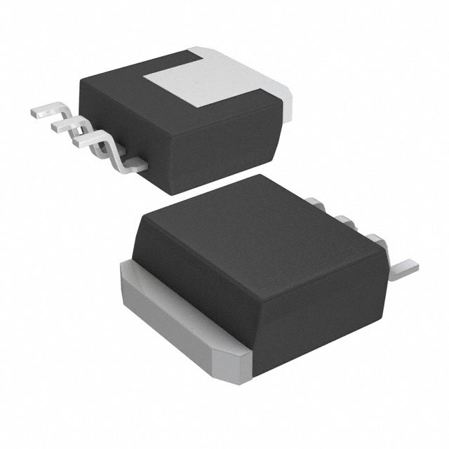
Fixed outputs of 5V and 8V are available in the
plastic TO-220 and SFM power packages.
Connection Diagrams
TO-220 Plastic Package
Figure 1. Front View
See Package Number NDE
SFM Plastic Surface-Mount Package
Figure 2. Top View
See Package Number KTT
Figure 3. Side View
See Package Number KTT
1
2
Please be aware that an important notice concerning availability, standard warranty, and use in critical applications of
Texas Instruments semiconductor products and disclaimers thereto appears at the end of this data sheet.
All trademarks are the property of their respective owners.
PRODUCTION DATA information is current as of publication date.
Products conform to specifications per the terms of the Texas
Instruments standard warranty. Production processing does not
necessarily include testing of all parameters.
Copyright © 1998–2013, Texas Instruments Incorporated
�LM2930
SNVS745D – APRIL 1998 – REVISED APRIL 2013
www.ti.com
These devices have limited built-in ESD protection. The leads should be shorted together or the device placed in conductive foam
during storage or handling to prevent electrostatic damage to the MOS gates.
Absolute Maximum Ratings (1) (2)
Input Voltage
Operating Range
26V
Overvoltage Protection
40V
−12V
Reverse Voltage (100 ms)
−6V
Reverse Voltage (DC)
Internal Power Dissipation
(3)
Internally Limited
−40°C to +85°C
Operating Temperature Range
Maximum Junction Temperature
125°C
−65°C to +150°C
Storage Temperature Range
Lead Temp. (Soldering, 10 seconds)
(1)
(2)
(3)
230°C
Absolute Maximum Ratings indicate limits beyond which damage to the device may occur. Operating ratings indicate conditions for
which the device is functional, but do not ensure specific performance limits. Electrical Characteristics state DC and AC electrical
specifications under particular test conditions which ensure specific performance limits. This assumes that the device is within the
Operating Ratings. Specifications are not ensured for parameters where no limit is given, however, the typical value is a good indication
of device performance.
If Military/Aerospace specified devices are required, please contact the Texas Instruments Sales Office/Distributors for availability and
specifications.
Thermal resistance without a heat sink for junction to case temperature is 3°C/W and for case to ambient temperature is 50°C/W for the
TO-220, 73°C/W for the SFM. If the SFM package is used, the thermal resistance can be reduced by increasing the P.C. board copper
area thermally connected to the package. Using 0.5 square inches of copper area, θJA is 50°C/W; with 1 square inch of copper area, θJA
is 37°C/W; and with 1.6 or more square inches of copper area, θJA is 32°C/W.
Electrical Characteristics (1)
LM2930-5.0 VIN=14V, IO=150 mA, Tj=25°C
Parameter
(2)
, C2=10 μF, unless otherwise specified
Conditions
Output Voltage
Typ
Tested
Limit (3)
5
5.3
VMAX
4.7
VMIN
6V≤VIN≤26V, 5 mA≤IO≤150 mA
−40°C≤TJ≤125°C
Line Regulation
Design
Limit (4)
5.5
4.5
Unit
VMAX
VMIN
9V≤VIN≤16V, IO=5 mA
7
25
mVMAX
6V≤VIN≤26V, IO=5 mA
30
80
mVMAX
Load Regulation
5 mA≤IO≤150 mA
14
50
mVMAX
Output Impedance
100 mADC & 10 mArms, 100 Hz−10 kHz
200
Quiescent Current
IO=10 mA
4
7
mAMAX
IO=150 mA
18
40
mAMAX
10 Hz−100 kHz
140
μVrms
20
mV/1000 hr
Output Noise Voltage
Long Term Stability
Ripple Rejection
fO=120 Hz
56
Current Limit
400
Dropout Voltage
IO=150 mA
Output Voltage Under
−12V≤VIN≤40V, RL=100Ω
0.32
Transient Conditions
(1)
(2)
(3)
(4)
2
mΩ
dB
700
mAMAX
150
mAMIN
0.6
VMAX
5.5
VMAX
−0.3
VMIN
All characteristics are measured with a capacitor across the input of 0.1 μF and a capacitor across the output of 10 μF. All
characteristics except noise voltage and ripple rejection ratio are measured using pulse techniques (tW≤10 ms, duty cycle≤5%). Output
voltage changes due to changes in internal temperature must be taken into account separately.
To ensure constant junction temperature, low duty cycle pulse testing is used.
Ensured and 100% production tested.
Ensured (but not 100% production tested) over the operating temperature and input current ranges. These limits are not used to
calculate outgoing quality levels.
Submit Documentation Feedback
Copyright © 1998–2013, Texas Instruments Incorporated
Product Folder Links: LM2930
�LM2930
www.ti.com
SNVS745D – APRIL 1998 – REVISED APRIL 2013
Electrical Characteristics (1)
(2)
, C2=10 μF, unless otherwise specified)
LM2930-8.0 (VIN=14V, IO=150 mA, Tj=25°C
Parameter
Conditions
Output Voltage
Typ
Tested
Limit (3)
8
8.5
Design
Limit (4)
Unit
VMAX
7.5
VMIN
9.4V≤VIN≤26V, 5 mA≤IO≤150 mA,
−40°C≤TJ≤125°C
Line Regulation
8.8
VMAX
7.2
VMIN
9.4V≤VIN≤16V, IO=5 mA
12
50
mVMAX
9.4V≤VIN≤26V, IO=5 mA
50
100
mVMAX
50
mVMAX
Load Regulation
5 mA≤IO≤150 mA
25
Output Impedance
100 mADC & 10 mArms, 100 Hz−10 kHz
300
Quiescent Current
IO=10 mA
4
7
mAMAX
IO=150 mA
18
40
mAMAX
10 Hz−100 kHz
170
μVrms
30
mV/1000 hr
52
dB
Output Noise Voltage
Long Term Stability
Ripple Rejection
fO=120 Hz
Current Limit
400
Dropout Voltage
IO=150 mA
0.32
Output Voltage Under
−12V≤VIN≤40V, RL=100Ω
Transient Conditions
(1)
(2)
(3)
(4)
mΩ
700
mAMAX
150
mAMIN
0.6
VMAX
8.8
VMAX
−0.3
VMIN
All characteristics are measured with a capacitor across the input of 0.1 μF and a capacitor across the output of 10 μF. All
characteristics except noise voltage and ripple rejection ratio are measured using pulse techniques (tW≤10 ms, duty cycle≤5%). Output
voltage changes due to changes in internal temperature must be taken into account separately.
To ensure constant junction temperature, low duty cycle pulse testing is used.
Ensured and 100% production tested.
Ensured (but not 100% production tested) over the operating temperature and input current ranges. These limits are not used to
calculate outgoing quality levels.
Typical Application
*Required if regulator is located far from power supply filter.
**COUT must be at least 10 μF to maintain stability. May be increased without bound to maintain regulation during
transients. Locate as close as possible to the regulator. This capacitor must be rated over the same operating
temperature range as the regulator. The equivalent series resistance (ESR) of this capacitor should be less than 1Ω
over the expected operating temperature range.
Submit Documentation Feedback
Copyright © 1998–2013, Texas Instruments Incorporated
Product Folder Links: LM2930
3
�LM2930
SNVS745D – APRIL 1998 – REVISED APRIL 2013
www.ti.com
Typical Performance Characteristics
4
Output Impedance
Overvoltage Supply Current
Figure 4.
Figure 5.
Reverse Supply Current
Output at Reverse
Supply
Figure 6.
Figure 7.
Output at Overvoltage
Output Voltage (Normalized to 1V at Tj=25°C)
Figure 8.
Figure 9.
Submit Documentation Feedback
Copyright © 1998–2013, Texas Instruments Incorporated
Product Folder Links: LM2930
�LM2930
www.ti.com
SNVS745D – APRIL 1998 – REVISED APRIL 2013
Typical Performance Characteristics (continued)
Dropout Voltage
Dropout Voltage
Figure 10.
Figure 11.
Low Voltage Behavior
High Voltage Behavior
Figure 12.
Figure 13.
Line Transient Response
Load Transient Response
Figure 14.
Figure 15.
Submit Documentation Feedback
Copyright © 1998–2013, Texas Instruments Incorporated
Product Folder Links: LM2930
5
�LM2930
SNVS745D – APRIL 1998 – REVISED APRIL 2013
www.ti.com
Typical Performance Characteristics (continued)
6
Peak Output Current
Quiescent Current
Figure 16.
Figure 17.
Quiescent Current
Quiescent Current
Figure 18.
Figure 19.
Ripple Rejection
Ripple Rejection
Figure 20.
Figure 21.
Submit Documentation Feedback
Copyright © 1998–2013, Texas Instruments Incorporated
Product Folder Links: LM2930
�LM2930
www.ti.com
SNVS745D – APRIL 1998 – REVISED APRIL 2013
Definition of Terms
Dropout Voltage: The input-output voltage differential at which the circuit ceases to regulate against further
reduction in input voltage. Measured when the output voltage has dropped 100 mV from the nominal value
obtained at 14V input, dropout voltage is dependent upon load current and junction temperature.
Input Voltage: The DC voltage applied to the input terminals with respect to ground.
Input-Output Differential: The voltage difference between the unregulated input voltage and the regulated
output voltage for which the regulator will operate.
Line Regulation: The change in output voltage for a change in the input voltage. The measurement is made
under conditions of low dissipation or by using pulse techniques such that the average chip temperature is not
significantly affected.
Load Regulation: The change in output voltage for a change in load current at constant chip temperature.
Long Term Stability: Output voltage stability under accelerated life-test conditions after 1000 hours with
maximum rated voltage and junction temperature.
Output Noise Voltage: The rms AC voltage at the output, with constant load and no input ripple, measured over
a specified frequency range.
Quiescent Current: That part of the positive input current that does not contribute to the positive load current.
The regulator ground lead current.
Ripple Rejection: The ratio of the peak-to-peak input ripple voltage to the peak-to-peak output ripple voltage.
Temperature Stability of VO: The percentage change in output voltage for a thermal variation from room
temperature to either temperature extreme.
Maximum Power Dissipation (TO-220)
(1)
Maximum Power Dissipation (SFM)
(1)
Thermal resistance without a heat sink for junction to case temperature is 3°C/W and for case to ambient temperature is 50°C/W for the
TO-220, 73°C/W for the SFM. If the SFM package is used, the thermal resistance can be reduced by increasing the P.C. board copper
area thermally connected to the package. Using 0.5 square inches of copper area, θJA is 50°C/W; with 1 square inch of copper area, θJA
is 37°C/W; and with 1.6 or more square inches of copper area, θJA is 32°C/W.
Submit Documentation Feedback
Copyright © 1998–2013, Texas Instruments Incorporated
Product Folder Links: LM2930
7
�LM2930
SNVS745D – APRIL 1998 – REVISED APRIL 2013
www.ti.com
Schematic Diagram
8
Submit Documentation Feedback
Copyright © 1998–2013, Texas Instruments Incorporated
Product Folder Links: LM2930
�LM2930
www.ti.com
SNVS745D – APRIL 1998 – REVISED APRIL 2013
REVISION HISTORY
Changes from Revision C (April 2013) to Revision D
•
Page
Changed layout of National Data Sheet to TI format ............................................................................................................ 8
Submit Documentation Feedback
Copyright © 1998–2013, Texas Instruments Incorporated
Product Folder Links: LM2930
9
�PACKAGE OPTION ADDENDUM
www.ti.com
1-Oct-2016
PACKAGING INFORMATION
Orderable Device
Status
(1)
Package Type Package Pins Package
Drawing
Qty
Eco Plan
Lead/Ball Finish
MSL Peak Temp
(2)
(6)
(3)
Op Temp (°C)
Device Marking
TBD
Call TI
Call TI
-40 to 85
LM2930T
-5.0 P+
Green (RoHS
& no Sb/Br)
CU SN
Level-1-NA-UNLIM
-40 to 85
LM2930T
-5.0 P+
(4/5)
LM2930T-5.0
OBSOLETE
TO-220
NDE
3
LM2930T-5.0/NOPB
ACTIVE
TO-220
NDE
3
LM2930T-8.0
OBSOLETE
TO-220
NDE
3
TBD
Call TI
Call TI
-40 to 85
LM2930T
8.0 P+
LM2930T-8.0/NOPB
OBSOLETE
TO-220
NDE
3
TBD
Call TI
Call TI
-40 to 85
LM2930T
8.0 P+
45
(1)
The marketing status values are defined as follows:
ACTIVE: Product device recommended for new designs.
LIFEBUY: TI has announced that the device will be discontinued, and a lifetime-buy period is in effect.
NRND: Not recommended for new designs. Device is in production to support existing customers, but TI does not recommend using this part in a new design.
PREVIEW: Device has been announced but is not in production. Samples may or may not be available.
OBSOLETE: TI has discontinued the production of the device.
(2)
Eco Plan - The planned eco-friendly classification: Pb-Free (RoHS), Pb-Free (RoHS Exempt), or Green (RoHS & no Sb/Br) - please check http://www.ti.com/productcontent for the latest availability
information and additional product content details.
TBD: The Pb-Free/Green conversion plan has not been defined.
Pb-Free (RoHS): TI's terms "Lead-Free" or "Pb-Free" mean semiconductor products that are compatible with the current RoHS requirements for all 6 substances, including the requirement that
lead not exceed 0.1% by weight in homogeneous materials. Where designed to be soldered at high temperatures, TI Pb-Free products are suitable for use in specified lead-free processes.
Pb-Free (RoHS Exempt): This component has a RoHS exemption for either 1) lead-based flip-chip solder bumps used between the die and package, or 2) lead-based die adhesive used between
the die and leadframe. The component is otherwise considered Pb-Free (RoHS compatible) as defined above.
Green (RoHS & no Sb/Br): TI defines "Green" to mean Pb-Free (RoHS compatible), and free of Bromine (Br) and Antimony (Sb) based flame retardants (Br or Sb do not exceed 0.1% by weight
in homogeneous material)
(3)
MSL, Peak Temp. - The Moisture Sensitivity Level rating according to the JEDEC industry standard classifications, and peak solder temperature.
(4)
There may be additional marking, which relates to the logo, the lot trace code information, or the environmental category on the device.
(5)
Multiple Device Markings will be inside parentheses. Only one Device Marking contained in parentheses and separated by a "~" will appear on a device. If a line is indented then it is a continuation
of the previous line and the two combined represent the entire Device Marking for that device.
(6)
Lead/Ball Finish - Orderable Devices may have multiple material finish options. Finish options are separated by a vertical ruled line. Lead/Ball Finish values may wrap to two lines if the finish
value exceeds the maximum column width.
Addendum-Page 1
Samples
�PACKAGE OPTION ADDENDUM
www.ti.com
1-Oct-2016
Important Information and Disclaimer:The information provided on this page represents TI's knowledge and belief as of the date that it is provided. TI bases its knowledge and belief on information
provided by third parties, and makes no representation or warranty as to the accuracy of such information. Efforts are underway to better integrate information from third parties. TI has taken and
continues to take reasonable steps to provide representative and accurate information but may not have conducted destructive testing or chemical analysis on incoming materials and chemicals.
TI and TI suppliers consider certain information to be proprietary, and thus CAS numbers and other limited information may not be available for release.
In no event shall TI's liability arising out of such information exceed the total purchase price of the TI part(s) at issue in this document sold by TI to Customer on an annual basis.
Addendum-Page 2
�MECHANICAL DATA
NDE0003B
www.ti.com
�IMPORTANT NOTICE
Texas Instruments Incorporated and its subsidiaries (TI) reserve the right to make corrections, enhancements, improvements and other
changes to its semiconductor products and services per JESD46, latest issue, and to discontinue any product or service per JESD48, latest
issue. Buyers should obtain the latest relevant information before placing orders and should verify that such information is current and
complete. All semiconductor products (also referred to herein as “components”) are sold subject to TI’s terms and conditions of sale
supplied at the time of order acknowledgment.
TI warrants performance of its components to the specifications applicable at the time of sale, in accordance with the warranty in TI’s terms
and conditions of sale of semiconductor products. Testing and other quality control techniques are used to the extent TI deems necessary
to support this warranty. Except where mandated by applicable law, testing of all parameters of each component is not necessarily
performed.
TI assumes no liability for applications assistance or the design of Buyers’ products. Buyers are responsible for their products and
applications using TI components. To minimize the risks associated with Buyers’ products and applications, Buyers should provide
adequate design and operating safeguards.
TI does not warrant or represent that any license, either express or implied, is granted under any patent right, copyright, mask work right, or
other intellectual property right relating to any combination, machine, or process in which TI components or services are used. Information
published by TI regarding third-party products or services does not constitute a license to use such products or services or a warranty or
endorsement thereof. Use of such information may require a license from a third party under the patents or other intellectual property of the
third party, or a license from TI under the patents or other intellectual property of TI.
Reproduction of significant portions of TI information in TI data books or data sheets is permissible only if reproduction is without alteration
and is accompanied by all associated warranties, conditions, limitations, and notices. TI is not responsible or liable for such altered
documentation. Information of third parties may be subject to additional restrictions.
Resale of TI components or services with statements different from or beyond the parameters stated by TI for that component or service
voids all express and any implied warranties for the associated TI component or service and is an unfair and deceptive business practice.
TI is not responsible or liable for any such statements.
Buyer acknowledges and agrees that it is solely responsible for compliance with all legal, regulatory and safety-related requirements
concerning its products, and any use of TI components in its applications, notwithstanding any applications-related information or support
that may be provided by TI. Buyer represents and agrees that it has all the necessary expertise to create and implement safeguards which
anticipate dangerous consequences of failures, monitor failures and their consequences, lessen the likelihood of failures that might cause
harm and take appropriate remedial actions. Buyer will fully indemnify TI and its representatives against any damages arising out of the use
of any TI components in safety-critical applications.
In some cases, TI components may be promoted specifically to facilitate safety-related applications. With such components, TI’s goal is to
help enable customers to design and create their own end-product solutions that meet applicable functional safety standards and
requirements. Nonetheless, such components are subject to these terms.
No TI components are authorized for use in FDA Class III (or similar life-critical medical equipment) unless authorized officers of the parties
have executed a special agreement specifically governing such use.
Only those TI components which TI has specifically designated as military grade or “enhanced plastic” are designed and intended for use in
military/aerospace applications or environments. Buyer acknowledges and agrees that any military or aerospace use of TI components
which have not been so designated is solely at the Buyer's risk, and that Buyer is solely responsible for compliance with all legal and
regulatory requirements in connection with such use.
TI has specifically designated certain components as meeting ISO/TS16949 requirements, mainly for automotive use. In any case of use of
non-designated products, TI will not be responsible for any failure to meet ISO/TS16949.
Products
Applications
Audio
www.ti.com/audio
Automotive and Transportation
www.ti.com/automotive
Amplifiers
amplifier.ti.com
Communications and Telecom
www.ti.com/communications
Data Converters
dataconverter.ti.com
Computers and Peripherals
www.ti.com/computers
DLP® Products
www.dlp.com
Consumer Electronics
www.ti.com/consumer-apps
DSP
dsp.ti.com
Energy and Lighting
www.ti.com/energy
Clocks and Timers
www.ti.com/clocks
Industrial
www.ti.com/industrial
Interface
interface.ti.com
Medical
www.ti.com/medical
Logic
logic.ti.com
Security
www.ti.com/security
Power Mgmt
power.ti.com
Space, Avionics and Defense
www.ti.com/space-avionics-defense
Microcontrollers
microcontroller.ti.com
Video and Imaging
www.ti.com/video
RFID
www.ti-rfid.com
OMAP Applications Processors
www.ti.com/omap
TI E2E Community
e2e.ti.com
Wireless Connectivity
www.ti.com/wirelessconnectivity
Mailing Address: Texas Instruments, Post Office Box 655303, Dallas, Texas 75265
Copyright © 2016, Texas Instruments Incorporated
�


 工商网监
湘ICP备2023018690号
工商网监
湘ICP备2023018690号
