LM2931-N
www.ti.com
SNOSBE5G – MARCH 2000 – REVISED APRIL 2013
LM2931-N Series Low Dropout Regulators
Check for Samples: LM2931-N
FEATURES
DESCRIPTION
•
•
•
•
•
•
•
•
•
•
The LM2931-N positive voltage regulator features a
very low quiescent current of 1mA or less when
supplying 10mA loads. This unique characteristic and
the extremely low input-output differential required for
proper regulation (0.2V for output currents of 10mA)
make the LM2931-N the ideal regulator for standby
power systems. Applications include memory standby
circuits, CMOS and other low power processor power
supplies as well as systems demanding as much as
100mA of output current.
1
2
•
Very Low Quiescent Current
Output Current in Excess of 100 mA
Input-output Differential Less than 0.6V
Reverse Battery Protection
60V Load Dump Protection
−50V Reverse Transient Protection
Short Circuit Protection
Internal Thermal Overload Protection
Mirror-image Insertion Protection
Available in TO-220, TO-92, TO-263, or SOIC-8
Packages
Available as Adjustable with TTL Compatible
Switch
Designed originally for automotive applications, the
LM2931-N and all regulated circuitry are protected
from reverse battery installations or 2 battery jumps.
During line transients, such as a load dump (60V)
when the input voltage to the regulator can
momentarily exceed the specified maximum
operating voltage, the regulator will automatically shut
down to protect both internal circuits and the load.
The LM2931-N cannot be harmed by temporary
mirror-image insertion. Familiar regulator features
such as short circuit and thermal overload protection
are also provided.
The LM2931-N family includes a fixed 5V output
(±3.8% tolerance for A grade) or an adjustable output
with ON/OFF pin. Both versions are available in a
TO-220 power package, DDPAK/TO-263 surface
mount package, and an 8-lead SOIC package. The
fixed output version is also available in the TO-92
plastic package.
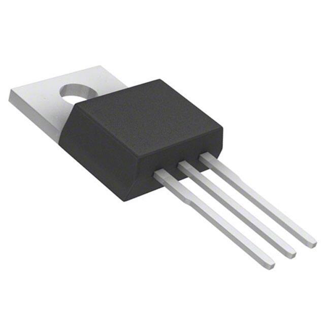
Connection Diagrams
FIXED VOLTAGE OUTPUT
Figure 1. TO-220 3-Lead Power Package
Front View
Figure 2. DDPAK/TO-263 Surface-Mount Package
Top View
Figure 3. Side View
1
2
Please be aware that an important notice concerning availability, standard warranty, and use in critical applications of
Texas Instruments semiconductor products and disclaimers thereto appears at the end of this data sheet.
All trademarks are the property of their respective owners.
PRODUCTION DATA information is current as of publication date.
Products conform to specifications per the terms of the Texas
Instruments standard warranty. Production processing does not
necessarily include testing of all parameters.
Copyright © 2000–2013, Texas Instruments Incorporated
�LM2931-N
SNOSBE5G – MARCH 2000 – REVISED APRIL 2013
www.ti.com
*NC = Not internally connected. Must be electrically isolated from the rest of the circuit for the DSBGA package.
Figure 4. 8-Pin SOIC
Top View
Figure 5. TO-92 Plastic Package
Bottom View
Figure 6. 6-Bump DSBGA
Top View
(Bump Side Down)
Figure 7. DSBGA Laser Mark
ADJUSTABLE OUTPUT VOLTAGE
Figure 8. TO-220 5-Lead Power Package
Front View
Figure 9. DDPAK/TO-263
5-Lead Surface-Mount Package
Top View
2
Submit Documentation Feedback
Figure 10. Side View
Copyright © 2000–2013, Texas Instruments Incorporated
Product Folder Links: LM2931-N
�LM2931-N
www.ti.com
SNOSBE5G – MARCH 2000 – REVISED APRIL 2013
Figure 11. 8-Pin SOIC
Top View
Typical Applications
*Required if regulator is located far from power supply filter.
**C2 must be at least 100 μF to maintain stability. May be increased without bound to maintain regulation during
transients. Locate as close as possible to the regulator. This capacitor must be rated over the same operating
temperature range as the regulator. The equivalent series resistance (ESR) of this capacitor is critical; see curve.
Figure 12. LM2931-N Fixed Output
Note: Using 27k for R1 will automatically compensate for errors in VOUT due to the input bias current of the ADJ pin
(approximately 1 μA).
Figure 13. LM2931-N Adjustable Output
Submit Documentation Feedback
Copyright © 2000–2013, Texas Instruments Incorporated
Product Folder Links: LM2931-N
3
�LM2931-N
SNOSBE5G – MARCH 2000 – REVISED APRIL 2013
www.ti.com
These devices have limited built-in ESD protection. The leads should be shorted together or the device placed in conductive foam
during storage or handling to prevent electrostatic damage to the MOS gates.
ABSOLUTE MAXIMUM RATINGS (1) (2)
Input Voltage
Operating Range
26V
Overvoltage Protection
LM2931A, LM2931C (Adjustable)
60V
LM2931-N
50V
Internal Power Dissipation
(3) (4)
Internally Limited
Operating Ambient Temperature
−40°C to +85°C
Range
Maximum Junction Temperature
125°C
−65°C to +150°C
Storage Temperature Range
Lead Temp. (Soldering, 10 seconds)
ESD Tolerance
(1)
(2)
(3)
(4)
(5)
230°C
(5)
2000V
Absolute Maximum Ratings indicate limits beyond which damage to the device may occur. Electrical specifications do not apply when
operating the device beyond its rated operating conditions.
If Military/Aerospace specified devices are required, please contact the Texas Instruments Sales Office/Distributors for availability and
specifications.
See circuit in Typical Applications. To ensure constant junction temperature, low duty cycle pulse testing is used.
The maximum power dissipation is a function of maximum junction temperature TJmax, total thermal resistance θJA, and ambient
temperature TA. The maximum allowable power dissipation at any ambient temperature is PD = (TJmax − TA)/θJA. If this dissipation is
exceeded, the die temperature will rise above 150°C and the LM2931-N will go into thermal shutdown. For the LM2931-N in the TO-92
package, θJA is 195°C/W; in the SOIC-8 package, θJA is 160°C/W, and in the TO-220 package, θJA is 50°C/W; in the DDPAK/TO-263
package, θJA is 73°C/W; and in the 6-Bump DSBGA package θJA is 290°C/W. If the TO-220 package is used with a heat sink, θJA is the
sum of the package thermal resistance junction-to-case of 3°C/W and the thermal resistance added by the heat sink and thermal
interface.If the TO-263 package is used, the thermal resistance can be reduced by increasing the P.C. board copper area thermally
connected to the package: Using 0.5 square inches of copper area, θJA is 50°C/W; with 1 square inch of copper area, θJA is 37°C/W;
and with 1.6 or more square inches of copper area, θJA is 32°C/W.
Human body model, 100 pF discharged through 1.5 kΩ.
ELECTRICAL CHARACTERISTICS FOR FIXED 3.3V VERSION
VIN = 14V, IO = 10mA, TJ = 25°C, C2 = 100μF (unless otherwise specified)
(1)
LM2931-N-3.3
Parameter
Conditions
Output Voltage
Typ
3.3
4V ≤ VIN ≤ 26V, IO = 100 mA
−40°C ≤ TJ ≤ 125°C
Limit
Units
3.465
3.135
VMAX
VMIN
3.630
2.970
VMAX
VMIN
(2)
Line Regulation
4V ≤ VIN ≤ 26V
4
33
mVMAX
Load Regulation
5mA ≤ IO ≤ 100mA
10
50
mVMAX
Output Impedance
100mADC and 10mArms,
100Hz - 10kHz
200
Quiescent Current
IO ≤ 10mA, 4V ≤ VIN ≤ 26V
0.4
mΩ
1.0
mAMAX
−40°C ≤ TJ ≤ 125°C
Output Noise Voltage
IO = 100mA, VIN = 14V, TJ = 25°C
15
10Hz -100kHz, COUT = 100μF
330
μVrms
13
mV/1000 hr
80
dB
Long Term Stability
Ripple Rejection
(1)
(2)
4
fO = 120Hz
mA
See circuit in Typical Applications. To ensure constant junction temperature, low duty cycle pulse testing is used.
All limits are specified for TJ = 25°C (standard type face) or over the full operating junction temperature range of −40°C to +125°C (bold
type face).
Submit Documentation Feedback
Copyright © 2000–2013, Texas Instruments Incorporated
Product Folder Links: LM2931-N
�LM2931-N
www.ti.com
SNOSBE5G – MARCH 2000 – REVISED APRIL 2013
ELECTRICAL CHARACTERISTICS FOR FIXED 3.3V VERSION (continued)
VIN = 14V, IO = 10mA, TJ = 25°C, C2 = 100μF (unless otherwise specified) (1)
LM2931-N-3.3
Parameter
Conditions
Dropout Voltage
Limit
Units
0.05
0.30
0.2
0.6
VMAX
Typ
IO = 10mA
IO = 100mA
Maximum Operational Input Voltage
(2)
33
26
VMIN
Maximum Line Transient
RL = 500Ω, VO ≤ 5.5V,
T = 1ms, τ ≤ 100ms
70
50
VMIN
Reverse Polarity Input Voltage, DC
VO ≥ −0.3V, RL = 500Ω
−30
−15
VMIN
Reverse Polarity Input Voltage,
Transient
T = 1ms, τ ≤ 100ms, RL = 500Ω
−80
−50
VMIN
ELECTRICAL CHARACTERISTICS FOR FIXED 5V VERSION
VIN = 14V, IO = 10mA, TJ = 25°C, C2 = 100 μF (unless otherwise specified)
(1)
LM2931A-5.0
Parameter
Conditions
Output Voltage
Typ
5
6.0V ≤ VIN ≤ 26V, IO = 100mA
−40°C ≤ TJ ≤ 125°C
Line Regulation
9V ≤ VIN ≤ 16V
6V ≤ VIN ≤ 26V
Load Regulation
Output Impedance
Quiescent Current
LM2931-N-5.0
Limit
Limit
Units
5.25
4.75
VMAX
VMIN
5.5
4.5
VMAX
VMIN
2
4
10
30
mVMAX
14
50
mVMAX
(2)
Typ
5.19
4.81
5
5.25
4.75
(2)
2
4
10
30
5 mA ≤ IO ≤ 100mA
14
50
100mADC and 10mArms,
100Hz -10kHz
200
IO ≤ 10mA, 6V ≤ VIN ≤ 26V
0.4
1.0
IO = 100mA, VIN = 14V, TJ = 25°C
15
30
10Hz -100kHz, COUT = 100μF
500
500
μVrms
20
20
mV/1000
hr
200
0.4
mΩ
1.0
mAMAX
−40°C ≤ TJ ≤ 125°C
Output Noise Voltage
Long Term Stability
15
mAMAX
Ripple Rejection
fO = 120 Hz
80
55
80
Dropout Voltage
IO = 10mA
IO = 100mA
0.05
0.3
0.2
0.6
0.05
0.3
0.2
0.6
VMAX
33
26
33
26
VMIN
Maximum Operational Input
Voltage
dBMIN
Maximum Line Transient
RL = 500Ω, VO ≤ 5.5V,
T = 1ms, τ ≤ 100ms
70
60
70
50
VMIN
Reverse Polarity Input Voltage,
DC
VO ≥ −0.3V, RL = 500Ω
−30
−15
−30
−15
VMIN
Reverse Polarity Input Voltage,
Transient
T = 1ms, τ ≤ 100ms, RL = 500Ω
−80
−50
−80
−50
VMIN
(1)
(2)
See circuit in Typical Applications. To ensure constant junction temperature, low duty cycle pulse testing is used.
All limits are specified for TJ = 25°C (standard type face) or over the full operating junction temperature range of −40°C to +125°C (bold
type face).
Submit Documentation Feedback
Copyright © 2000–2013, Texas Instruments Incorporated
Product Folder Links: LM2931-N
5
�LM2931-N
SNOSBE5G – MARCH 2000 – REVISED APRIL 2013
www.ti.com
ELECTRICAL CHARACTERISTICS FOR ADJUSTABLE VERSION
VIN = 14V, VOUT = 3V, IO = 10 mA, TJ = 25°C, R1 = 27k, C2 = 100 μF (unless otherwise specified)
Parameter
Conditions
Reference Voltage
(1)
Typ
Limit
Units Limit
1.20
1.26
VMAX
1.14
VMIN
IO ≤ 100 mA, −40°C ≤ Tj ≤ 125°C, R1 = 27k
1.32
VMAX
Measured from VOUT to Adjust Pin
1.08
VMIN
24
VMAX
Output Voltage Range
3
VMIN
mV/VMAX
Line Regulation
VOUT + 0.6V ≤ VIN ≤ 26V
0.2
1.5
Load Regulation
5 mA ≤ IO ≤ 100 mA
0.3
1
Output Impedance
100 mADC and 10 mArms, 100 Hz–10 kHz
40
Quiescent Current
IO = 10 mA
0.4
Output Noise Voltage
%MAX
mΩ/V
1
mAMAX
1
mAMAX
IO = 100 mA
15
During Shutdown RL = 500Ω
0.8
10 Hz–100 kHz
100
μVrms/V
0.4
%/1000 hr
Long Term Stability
mA
Ripple Rejection
fO = 120 Hz
0.02
Dropout Voltage
IO ≤ 10 mA
0.05
0.2
VMAX
%/V
IO = 100 mA
0.3
0.6
VMAX
33
26
VMIN
70
60
VMIN
−30
−15
VMIN
−80
−50
VMIN
On
2.0
1.2
VMAX
Off
2.2
3.25
VMIN
20
50
μAMAX
Maximum Operational Input
Voltage
Maximum Line Transient
IO = 10 mA, Reference Voltage ≤ 1.5V
T = 1 ms, τ ≤ 100 ms
Reverse Polarity Input
VO ≥ −0.3V, RL = 500Ω
Voltage, DC
Reverse Polarity Input
T = 1 ms, τ ≤ 100 ms, RL = 500Ω
Voltage, Transient
On/Off Threshold Voltage
VO=3V
On/Off Threshold Current
(1)
6
See circuit in Typical Applications. To ensure constant junction temperature, low duty cycle pulse testing is used.
Submit Documentation Feedback
Copyright © 2000–2013, Texas Instruments Incorporated
Product Folder Links: LM2931-N
�LM2931-N
www.ti.com
SNOSBE5G – MARCH 2000 – REVISED APRIL 2013
TYPICAL PERFORMANCE CHARACTERISTICS
Dropout Voltage
Dropout Voltage
Figure 14.
Figure 15.
Low Voltage Behavior
Output at Voltage Extremes
Figure 16.
Figure 17.
Line Transient Response
Load Transient Response
Figure 18.
Figure 19.
Submit Documentation Feedback
Copyright © 2000–2013, Texas Instruments Incorporated
Product Folder Links: LM2931-N
7
�LM2931-N
SNOSBE5G – MARCH 2000 – REVISED APRIL 2013
www.ti.com
TYPICAL PERFORMANCE CHARACTERISTICS (continued)
8
Peak Output Current
Quiescent Current
Figure 20.
Figure 21.
Quiescent Current
Quiescent Current
Figure 22.
Figure 23.
Ripple Rejection
Ripple Rejection
Figure 24.
Figure 25.
Submit Documentation Feedback
Copyright © 2000–2013, Texas Instruments Incorporated
Product Folder Links: LM2931-N
�LM2931-N
www.ti.com
SNOSBE5G – MARCH 2000 – REVISED APRIL 2013
TYPICAL PERFORMANCE CHARACTERISTICS (continued)
Output Impedance
Operation During Load
Dump
Figure 26.
Figure 27.
Reference Voltage
Maximum Power Dissipation
(SOIC-8)
Figure 28.
Figure 29.
Maximum Power Dissipation
(TO-220)
Maximum Power Dissipation
(TO-92)
Figure 30.
Figure 31.
Submit Documentation Feedback
Copyright © 2000–2013, Texas Instruments Incorporated
Product Folder Links: LM2931-N
9
�LM2931-N
SNOSBE5G – MARCH 2000 – REVISED APRIL 2013
www.ti.com
TYPICAL PERFORMANCE CHARACTERISTICS (continued)
Maximum Power Dissipation
(TO-263) (1)
On/Off Threshold
Figure 32.
Figure 33.
Output Capacitor ESR
Figure 34.
(1)
10
The maximum power dissipation is a function of maximum junction temperature TJmax, total thermal resistance θJA, and ambient
temperature TA. The maximum allowable power dissipation at any ambient temperature is PD = (TJmax − TA)/θJA. If this dissipation is
exceeded, the die temperature will rise above 150°C and the LM2931-N will go into thermal shutdown. For the LM2931-N in the TO-92
package, θJA is 195°C/W; in the SOIC-8 package, θJA is 160°C/W, and in the TO-220 package, θJA is 50°C/W; in the DDPAK/TO-263
package, θJA is 73°C/W; and in the 6-Bump DSBGA package θJA is 290°C/W. If the TO-220 package is used with a heat sink, θJA is the
sum of the package thermal resistance junction-to-case of 3°C/W and the thermal resistance added by the heat sink and thermal
interface.If the TO-263 package is used, the thermal resistance can be reduced by increasing the P.C. board copper area thermally
connected to the package: Using 0.5 square inches of copper area, θJA is 50°C/W; with 1 square inch of copper area, θJA is 37°C/W;
and with 1.6 or more square inches of copper area, θJA is 32°C/W.
Submit Documentation Feedback
Copyright © 2000–2013, Texas Instruments Incorporated
Product Folder Links: LM2931-N
�LM2931-N
www.ti.com
SNOSBE5G – MARCH 2000 – REVISED APRIL 2013
SCHEMATIC DIAGRAM
Submit Documentation Feedback
Copyright © 2000–2013, Texas Instruments Incorporated
Product Folder Links: LM2931-N
11
�LM2931-N
SNOSBE5G – MARCH 2000 – REVISED APRIL 2013
www.ti.com
APPLICATION HINTS
One of the distinguishing factors of the LM2931-N series regulators is the requirement of an output capacitor for
device stability. The value required varies greatly depending upon the application circuit and other factors. Thus
some comments on the characteristics of both capacitors and the regulator are in order.
High frequency characteristics of electrolytic capacitors depend greatly on the type and even the manufacturer.
As a result, a value of capacitance that works well with the LM2931-N for one brand or type may not necessary
be sufficient with an electrolytic of different origin. Sometimes actual bench testing, as described later, will be the
only means to determine the proper capacitor type and value. Experience has shown that, as a rule of thumb, the
more expensive and higher quality electrolytics generally allow a smaller value for regulator stability. As an
example, while a high-quality 100 μF aluminum electrolytic covers all general application circuits, similar stability
can be obtained with a tantalum electrolytic of only 47μF. This factor of two can generally be applied to any
special application circuit also.
Another critical characteristic of electrolytics is their performance over temperature. While the LM2931-N is
designed to operate to −40°C, the same is not always true with all electrolytics (hot is generally not a problem).
The electrolyte in many aluminum types will freeze around −30°C, reducing their effective value to zero. Since
the capacitance is needed for regulator stability, the natural result is oscillation (and lots of it) at the regulator
output. For all application circuits where cold operation is necessary, the output capacitor must be rated to
operate at the minimum temperature. By coincidence, worst-case stability for the LM2931-N also occurs at
minimum temperatures. As a result, in applications where the regulator junction temperature will never be less
than 25°C, the output capacitor can be reduced approximately by a factor of two over the value needed for the
entire temperature range. To continue our example with the tantalum electrolytic, a value of only 22μF would
probably thus suffice. For high-quality aluminum, 47μF would be adequate in such an application.
Another regulator characteristic that is noteworthy is that stability decreases with higher output currents. This
sensible fact has important connotations. In many applications, the LM2931-N is operated at only a few milliamps
of output current or less. In such a circuit, the output capacitor can be further reduced in value. As a rough
estimation, a circuit that is required to deliver a maximum of 10mA of output current from the regulator would
need an output capacitor of only half the value compared to the same regulator required to deliver the full output
current of 100mA. If the example of the tantalum capacitor in the circuit rated at 25°C junction temperature and
above were continued to include a maximum of 10mA of output current, then the 22μF output capacitor could be
reduced to only 10μF.
In the case of the LM2931CT adjustable regulator, the minimum value of output capacitance is a function of the
output voltage. As a general rule, the value decreases with higher output voltages, since internal loop gain is
reduced.
At this point, the procedure for bench testing the minimum value of an output capacitor in a special application
circuit should be clear. Since worst-case occurs at minimum operating temperatures and maximum operating
currents, the entire circuit, including the electrolytic, should be cooled to the minimum temperature. The input
voltage to the regulator should be maintained at 0.6V above the output to keep internal power dissipation and die
heating to a minimum. Worst-case occurs just after input power is applied and before the die has had a chance
to heat up. Once the minimum value of capacitance has been found for the brand and type of electrolytic in
question, the value should be doubled for actual use to account for production variations both in the capacitor
and the regulator. (All the values in this section and the remainder of the data sheet were determined in this
fashion.)
LM2931-N DSBGA Light Sensitivity
When the LM2931-N DSBGA package is exposed to bright sunlight, normal office fluorescent light, and other
LED's, it operates within the limits specified in the electrical characteristic table.
12
Submit Documentation Feedback
Copyright © 2000–2013, Texas Instruments Incorporated
Product Folder Links: LM2931-N
�LM2931-N
www.ti.com
SNOSBE5G – MARCH 2000 – REVISED APRIL 2013
Definition of Terms
Dropout Voltage: The input-output voltage differential at which the circuit ceases to regulate against further
reduction in input voltage. Measured when the output voltage has dropped 100 mV from the nominal value
obtained at 14V input, dropout voltage is dependent upon load current and junction temperature.
Input Voltage: The DC voltage applied to the input terminals with respect to ground.
Input-Output Differential: The voltage difference between the unregulated input voltage and the regulated
output voltage for which the regulator will operate.
Line Regulation: The change in output voltage for a change in the input voltage. The measurement is made
under conditions of low dissipation or by using pulse techniques such that the average chip temperature is
not significantly affected.
Load Regulation: The change in output voltage for a change in load current at constant chip temperature.
Long Term Stability: Output voltage stability under accelerated life-test conditions after 1000 hours with
maximum rated voltage and junction temperature.
Output Noise Voltage: The rms AC voltage at the output, with constant load and no input ripple, measured
over a specified frequency range.
Quiescent Current: That part of the positive input current that does not contribute to the positive load current.
The regulator ground lead current.
Ripple Rejection: The ratio of the peak-to-peak input ripple voltage to the peak-to-peak output ripple voltage at
a specified frequency.
Temperature Stability of VO: The percentage change in output voltage for a thermal variation from room
temperature to either temperature extreme.
Submit Documentation Feedback
Copyright © 2000–2013, Texas Instruments Incorporated
Product Folder Links: LM2931-N
13
�LM2931-N
SNOSBE5G – MARCH 2000 – REVISED APRIL 2013
www.ti.com
REVISION HISTORY
Changes from Revision F (April 2013) to Revision G
•
14
Page
Changed layout of National Data Sheet to TI format .......................................................................................................... 13
Submit Documentation Feedback
Copyright © 2000–2013, Texas Instruments Incorporated
Product Folder Links: LM2931-N
�PACKAGE OPTION ADDENDUM
www.ti.com
9-Apr-2022
PACKAGING INFORMATION
Orderable Device
Status
(1)
Package Type Package Pins Package
Drawing
Qty
Eco Plan
(2)
Lead finish/
Ball material
MSL Peak Temp
Op Temp (°C)
Device Marking
(3)
(4/5)
(6)
LM2931AM-5.0
NRND
SOIC
D
8
95
Non-RoHS
& Green
Call TI
Level-1-235C-UNLIM
-40 to 85
2931A
M-5.0
LM2931AM-5.0/NOPB
ACTIVE
SOIC
D
8
95
RoHS & Green
SN
Level-1-260C-UNLIM
-40 to 85
2931A
M-5.0
LM2931AMX-5.0/NOPB
ACTIVE
SOIC
D
8
2500
RoHS & Green
SN
Level-1-260C-UNLIM
-40 to 85
2931A
M-5.0
LM2931AS-5.0
NRND
DDPAK/
TO-263
KTT
3
45
Non-RoHS
& Green
Call TI
Level-3-235C-168 HR
-40 to 85
LM2931
AS5.0
LM2931AS-5.0/NOPB
ACTIVE
DDPAK/
TO-263
KTT
3
45
RoHS-Exempt
& Green
SN
Level-3-245C-168 HR
-40 to 85
LM2931
AS5.0
LM2931ASX-5.0
NRND
DDPAK/
TO-263
KTT
3
500
Non-RoHS
& Green
Call TI
Level-3-235C-168 HR
-40 to 85
LM2931
AS5.0
LM2931ASX-5.0/NOPB
ACTIVE
DDPAK/
TO-263
KTT
3
500
RoHS-Exempt
& Green
SN
Level-3-245C-168 HR
-40 to 85
LM2931
AS5.0
LM2931AT-5.0
NRND
TO-220
NDE
3
45
Non-RoHS
& Green
Call TI
Level-1-NA-UNLIM
-40 to 85
LM2931
AT5.0
LM2931AT-5.0/NOPB
ACTIVE
TO-220
NDE
3
45
RoHS & Green
SN
Level-1-NA-UNLIM
-40 to 85
LM2931
AT5.0
LM2931AZ-5.0/LFT1
ACTIVE
TO-92
LP
3
2000
RoHS & Green
Call TI
N / A for Pkg Type
-40 to 85
LM293
1AZ-5
LM2931AZ-5.0/LFT3
ACTIVE
TO-92
LP
3
2000
RoHS & Green
Call TI
N / A for Pkg Type
-40 to 85
LM293
1AZ-5
LM2931AZ-5.0/LFT4
ACTIVE
TO-92
LP
3
2000
RoHS & Green
Call TI
N / A for Pkg Type
-40 to 85
LM293
1AZ-5
LM2931AZ-5.0/NOPB
ACTIVE
TO-92
LP
3
1800
RoHS & Green
Call TI
N / A for Pkg Type
-40 to 85
LM293
1AZ-5
LM2931CM
NRND
SOIC
D
8
95
Non-RoHS
& Green
Call TI
Level-1-235C-UNLIM
-40 to 85
LM29
31CM
LM2931CM/NOPB
ACTIVE
SOIC
D
8
95
RoHS & Green
SN
Level-1-260C-UNLIM
-40 to 85
LM29
31CM
LM2931CMX
NRND
SOIC
D
8
2500
Non-RoHS
& Green
Call TI
Level-1-235C-UNLIM
-40 to 85
LM29
31CM
LM2931CMX/NOPB
ACTIVE
SOIC
D
8
2500
RoHS & Green
SN
Level-1-260C-UNLIM
-40 to 85
LM29
Addendum-Page 1
Samples
�PACKAGE OPTION ADDENDUM
www.ti.com
9-Apr-2022
Orderable Device
Status
(1)
Package Type Package Pins Package
Drawing
Qty
Eco Plan
(2)
Lead finish/
Ball material
MSL Peak Temp
Op Temp (°C)
Device Marking
(3)
(4/5)
(6)
31CM
LM2931CS
NRND
DDPAK/
TO-263
KTT
5
45
Non-RoHS
& Green
Call TI
Level-3-235C-168 HR
-40 to 85
LM2931CS
LM2931CS/NOPB
ACTIVE
DDPAK/
TO-263
KTT
5
45
RoHS-Exempt
& Green
SN
Level-3-245C-168 HR
-40 to 85
LM2931CS
LM2931CT/NOPB
ACTIVE
TO-220
KC
5
45
RoHS & Green
SN
Level-1-NA-UNLIM
-40 to 85
LM2931CT
LM2931M-5.0
NRND
SOIC
D
8
95
Non-RoHS
& Green
Call TI
Level-1-235C-UNLIM
-40 to 85
2931
M-5.0
LM2931M-5.0/NOPB
ACTIVE
SOIC
D
8
95
RoHS & Green
SN
Level-1-260C-UNLIM
-40 to 85
2931
M-5.0
LM2931MX-5.0
NRND
SOIC
D
8
2500
Non-RoHS
& Green
Call TI
Level-1-235C-UNLIM
-40 to 85
2931
M-5.0
LM2931MX-5.0/NOPB
ACTIVE
SOIC
D
8
2500
RoHS & Green
SN
Level-1-260C-UNLIM
-40 to 85
2931
M-5.0
LM2931S-5.0/NOPB
ACTIVE
DDPAK/
TO-263
KTT
3
45
RoHS-Exempt
& Green
SN
Level-3-245C-168 HR
-40 to 85
LM2931S
5.0
LM2931T-5.0/NOPB
ACTIVE
TO-220
NDE
3
45
RoHS & Green
SN
Level-1-NA-UNLIM
-40 to 85
LM2931T
5.0
LM2931Z-5.0/LFT2
ACTIVE
TO-92
LP
3
2000
RoHS & Green
SN
N / A for Pkg Type
-40 to 85
LM293
1Z-5
LM2931Z-5.0/NOPB
ACTIVE
TO-92
LP
3
1800
RoHS & Green
Call TI
N / A for Pkg Type
-40 to 85
LM293
1Z-5
(1)
The marketing status values are defined as follows:
ACTIVE: Product device recommended for new designs.
LIFEBUY: TI has announced that the device will be discontinued, and a lifetime-buy period is in effect.
NRND: Not recommended for new designs. Device is in production to support existing customers, but TI does not recommend using this part in a new design.
PREVIEW: Device has been announced but is not in production. Samples may or may not be available.
OBSOLETE: TI has discontinued the production of the device.
(2)
RoHS: TI defines "RoHS" to mean semiconductor products that are compliant with the current EU RoHS requirements for all 10 RoHS substances, including the requirement that RoHS substance
do not exceed 0.1% by weight in homogeneous materials. Where designed to be soldered at high temperatures, "RoHS" products are suitable for use in specified lead-free processes. TI may
reference these types of products as "Pb-Free".
RoHS Exempt: TI defines "RoHS Exempt" to mean products that contain lead but are compliant with EU RoHS pursuant to a specific EU RoHS exemption.
Green: TI defines "Green" to mean the content of Chlorine (Cl) and Bromine (Br) based flame retardants meet JS709B low halogen requirements of


 工商网监
湘ICP备2023018690号
工商网监
湘ICP备2023018690号
