Sample &
Buy
Product
Folder
Support &
Community
Tools &
Software
Technical
Documents
LM2937
SNVS100F – MARCH 2000 – REVISED JULY 2014
LM2937 500-mA Low Dropout Regulator
1 Features
•
•
•
1
•
•
•
•
•
•
3 Description
Fully Specified for Operation Over −40°C to 125°C
Output Current in Excess of 500 mA
Output Trimmed for 5% Tolerance Under all
Operating Conditions
Typical Dropout Voltage of 0.5 V at Full Rated
Load Current
Wide Output Capacitor ESR Range, up to 3 Ω
Internal Short Circuit and Thermal Overload
Protection
Reverse Battery Protection
60-V Input Transient Protection
Mirror Image Insertion Protection
2 Applications
•
•
•
Automotive
Industrial Control
Point-of-Load regulation
space
space
space
Simplified Schematic
The LM2937 is a positive voltage regulator capable of
supplying up to 500 mA of load current. The use of a
PNP power transistor provides a low dropout voltage
characteristic. With a load current of 500 mA the
minimum input to output voltage differential required
for the output to remain in regulation is typically 0.5 V
(1-V ensured maximum over the full operating
temperature range). Special circuitry has been
incorporated to minimize the quiescent current to
typically only 10 mA with a full 500-mA load current
when the input to output voltage differential is greater
than 3 V.
The LM2937 requires an output bypass capacitor for
stability. As with most low dropout regulators, the
ESR of this capacitor remains a critical design
parameter, but the LM2937 includes special
compensation
circuitry
that
relaxes
ESR
requirements. The device is stable for all ESR below
3 Ω. This allows the use of low ESR chip capacitors.
Ideally suited for automotive applications, the LM2937
will protect itself and any load circuitry from reverse
battery connections, two-battery jumps, and up to 60V/−50-V load dump transients. Familiar regulator
features such as short circuit and thermal shutdown
protection are also built in.
Device Information(1)
PART
NUMBER
LM2937
PACKAGE
BODY SIZE (NOM)
TO-220 (3)
14.986 mm x 10.66 mm
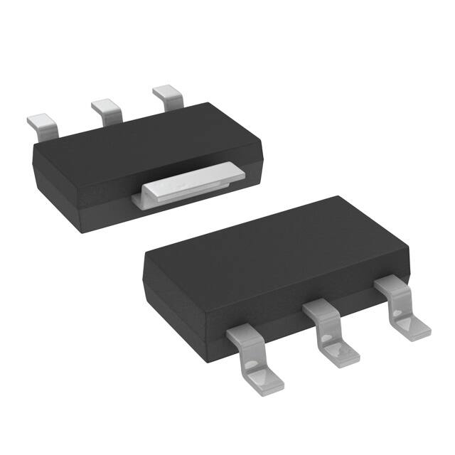
SOT (4)
6.50 mm x 3.5 mm
TO-263 (3)
10.18 mm x 8.41 mm
(1) For all available packages, see the orderable addendum at
the end of the datasheet.
1
An IMPORTANT NOTICE at the end of this data sheet addresses availability, warranty, changes, use in safety-critical applications,
intellectual property matters and other important disclaimers. PRODUCTION DATA.
�LM2937
SNVS100F – MARCH 2000 – REVISED JULY 2014
www.ti.com
Table of Contents
1
2
3
4
5
6
7
Features ..................................................................
Applications ...........................................................
Description .............................................................
Revision History.....................................................
Pin Configuration and Functions .........................
Specifications.........................................................
1
1
1
2
3
4
6.1
6.2
6.3
6.4
6.5
6.6
6.7
6.8
6.9
6.10
4
4
4
4
5
5
5
7
7
8
Absolute Maximum Ratings ......................................
Handling Ratings ......................................................
Recommended Operating Conditions.......................
Thermal Information ..................................................
Electrical Characteristics: LM2937-5 ........................
Electrical Characteristics: LM2937-8 ........................
Electrical Characteristics: LM2937-10 ......................
Electrical Characteristics: LM2937-12 ......................
Electrical Characteristics: LM2937-15 ......................
Typical Characteristics ............................................
Detailed Description ............................................ 11
7.1
7.2
7.3
7.4
8
Overview .................................................................
Functional Block Diagram .......................................
Feature Description.................................................
Device Functional Modes........................................
11
11
11
12
Application and Implementation ........................ 13
8.1 Application Information............................................ 13
8.2 Typical Application ................................................. 13
9 Power Supply Recommendations...................... 17
10 Layout................................................................... 18
10.1 Layout Guidelines ................................................. 18
10.2 Layout Example .................................................... 18
11 Device and Documentation Support ................. 19
11.1 Trademarks ........................................................... 19
11.2 Electrostatic Discharge Caution ............................ 19
11.3 Glossary ................................................................ 19
12 Mechanical, Packaging, and Orderable
Information ........................................................... 19
4 Revision History
NOTE: Page numbers for previous revisions may differ from page numbers in the current version.
Changes from Revision E (June 2013) to Revision F
•
2
Page
Changed format to meet new TI standards; added Device Information and Handling Ratings tables; updated
connection drawings; rename Functional Description and Applications sections, reformat and add new information,
add Devices and Documentation section .............................................................................................................................. 1
Submit Documentation Feedback
Copyright © 2000–2014, Texas Instruments Incorporated
Product Folder Links: LM2937
�LM2937
www.ti.com
SNVS100F – MARCH 2000 – REVISED JULY 2014
5 Pin Configuration and Functions
TO-220 Plastic Package (NDE)
3
Top View
INPUT
1
GND
2
OUTPUT
3
TAB
SOT-223 Plastic Package (DCY)
4
Top View
INPUT
1
GND
2
OUTPUT
3
4
(TAB)
DDPAK/TO-263 Surface-Mount Package (KTT)
3
Top View
1
GND
2
OUTPUT
3
TAB
INPUT
Pin Functions
PIN
I/O
DESCRIPTION
NAME
NDE
KTT
DCY
INPUT
1
1
1
I
GND
2
2
2
—
Ground
OUTPUT
3
3
3
O
Regulated voltage output. This pin requires an output capacitor to
maintain stability. See the Detailed Design Procedure section for output
capacitor details.
—
Thermal and ground connection. Connect the TAB to a large copper
area to remove heat from the device. The TAB is internally connected
to device pin 2 (GND). Connect the TAB to GND or leave floating. Do
not connect the TAB to any potential other than GND at device pin 2.
GND
TAB
TAB
4
Unregulated voltage input
Submit Documentation Feedback
Copyright © 2000–2014, Texas Instruments Incorporated
Product Folder Links: LM2937
3
�LM2937
SNVS100F – MARCH 2000 – REVISED JULY 2014
www.ti.com
6 Specifications
6.1 Absolute Maximum Ratings (1) (2)
over operating free-air temperature range (unless otherwise noted)
MIN
Input voltage (VIN)
MAX
Continuous
26
Transient (t ≤ 100 ms)
60
Internal power dissipation (3)
(2)
(3)
V
Internally limited
Maximum junction temperature
(1)
UNIT
150
°C
Stresses beyond those listed under Absolute Maximum Ratings may cause permanent damage to the device. These are stress ratings
only, which do not imply functional operation of the device at these or any other conditions beyond those indicated under Recommended
Operating Conditions. Exposure to absolute-maximum-rated conditions for extended periods may affect device reliability.
If Military/Aerospace specified devices are required, please contact the Texas Instruments Sales Office/Distributors for availability and
specifications.
The maximum allowable power dissipation at any ambient temperature is PMAX = (125°C − TA)/RθJA, where 125 is the maximum junction
temperature for operation, TA is the ambient temperature, and RθJA is the junction-to-ambient thermal resistance. If this dissipation is
exceeded, the die temperature will rise above 125°C and the electrical specifications do not apply. If the die temperature rises above
150°C, the LM2937 will go into thermal shutdown.
6.2 Handling Ratings
Tstg
Storage temperature range
V(ESD)
(1)
Electrostatic discharge
Human body model (HBM), per ANSI/ESDA/JEDEC JS-001, all
pins (1)
MIN
MAX
UNIT
−65
150
°C
–2000
2000
V
JEDEC document JEP155 states that 500-V HBM allows safe manufacturing with a standard ESD control process.
6.3 Recommended Operating Conditions (1)
over operating free-air temperature range (unless otherwise noted)
MIN
Junction temperature (TJ)
(2)
(2)
MAX
LM2937ET (NDE), LM2937ES (KTT)
−40
125
LM2937IMP (DCY)
−40
85
VOUT + 1V
26
Input voltage (VIN)
(1)
NOM
UNIT
°C
V
Stresses beyond those listed under Absolute Maximum Ratings may cause permanent damage to the device. These are stress ratings
only, which do not imply functional operation of the device at these or any other conditions beyond those indicated under Recommended
Operating Conditions. Exposure to absolute-maximum-rated conditions for extended periods may affect device reliability.
The maximum allowable power dissipation at any ambient temperature is PMAX = (125°C − TA)/RθJA, where 125°C is the maximum
junction temperature for operation, TA is the ambient temperature, and RθJA is the junction-to-ambient thermal resistance. If this
dissipation is exceeded, the die temperature will rise above 125°C and the electrical specifications do not apply. If the die temperature
rises above 150°C, the LM2937 will go into thermal shutdown.
6.4 Thermal Information
LM2937
THERMAL METRIC (1)
NDE (2)
KTT
DCY
3 PINS
3 PINS
4 PINS
RθJA
Junction-to-ambient thermal resistance
77.9
41.8
58.3
RθJC(top)
Junction-to-case (top) thermal resistance
35.5
43.5
39.2
RθJB
Junction-to-board thermal resistance
70.6
0.8
N/A
ψJT
Junction-to-top characterization parameter
13
23.5
7
ψJB
Junction-to-board characterization parameter
70.6
10.3
1.6
RθJC(bot)
Junction-to-case (bottom) thermal resistance
1
22.5
22.5
(1)
(2)
4
UNIT
°C/W
For more information about traditional and new thermal metrics, see the IC Package Thermal Metrics application report, SPRA953.
Thermal information for the TO-220 package is for a free-standing package vertically mounted in the middle of a PCB which is compliant
to the JEDEC HIGH-K 2s2p (JESD51-7) specifications. No additional heat sink is attached. See Heatsinking TO-220 Package Parts
section for more information.
Submit Documentation Feedback
Copyright © 2000–2014, Texas Instruments Incorporated
Product Folder Links: LM2937
�LM2937
www.ti.com
SNVS100F – MARCH 2000 – REVISED JULY 2014
6.5 Electrical Characteristics: LM2937-5
Unless otherwise specified: VIN = VOUT(NOM) + 5 V; IOUT(MAX) = 500 mA for the TO-220 and DDPAK/TO-263 packages; IOUT(MAX)
= 400 mA for the SOT-223 package; and COUT = 10 μF. Conditions and the associated minimum and maximum limits apply
over the Recommended Operating temperature range for the specific package, unless otherwise noted.
PARAMETER
Output voltage
MIN
TYP
MAX
UNIT
TA = TJ = 25°C, 5 mA ≤ IOUT ≤ IOUT(MAX)
CONDITIONS
4.85
5
5.15
V
5 mA ≤ IOUT ≤ IOUT(MAX)
4.75
5
5.25
V
Line regulation
(VOUT + 2 V) ≤ VIN ≤ 26 V, IOUT = 5 mA
15
50
mV
Load regulation
5 mA ≤ IOUT ≤ IOUT(MAX)
5
50
mV
Quiescent Current
(VOUT + 2 V) ≤ VIN ≤ 26 V, IOUT = 5 mA
2
10
mA
10
20
VIN = (VOUT + 5 V), IOUT = IOUT(MAX)
10 Hz to 100 kHz, IOUT = 5 mA
Long-term stability
1000 Hrs.
20
Dropout voltage
IOUT = IOUT(MAX)
0.5
1
150
110
250
IOUT = 50 mA
Short-circuit current
Peak line transient voltage
tf < 100 ms, RL = 100 Ω
Maximum operational input voltage
mA
μVrms
Output noise voltage
mV
V
mV
0.6
1
A
60
75
V
26
V
Reverse DC input voltage
VOUT ≥ −0.6 V, RL = 100 Ω
–15
–30
V
Reverse transient input voltage
tr < 1 ms, RL = 100 Ω
–50
–75
V
6.6 Electrical Characteristics: LM2937-8
Unless otherwise specified: VIN = VOUT(NOM) + 5 V; IOUT(MAX) = 500 mA for the TO-220 and DDPAK/TO-263 packages; IOUT(MAX)
= 400 mA for the SOT-223 package; and COUT = 10 μF. Conditions and the associated Minimum and Maximum limits apply
over the Recommended Operating temperature range for the specific package, unless otherwise noted.
PARAMETER
Output voltage
CONDITIONS
TA = TJ = 25°C, 5 mA ≤ IOUT ≤ IOUT(MAX)
5 mA ≤ IOUT ≤ IOUT(MAX)
Line regulation
(VOUT + 2 V) ≤ VIN ≤ 26 V, IOUT = 5 mA
Load regulation
5 mA ≤ IOUT ≤ IOUT(MAX)
Quiescent Current
(VOUT + 2 V) ≤ VIN ≤ 26 V, IOUT = 5 mA
MIN
TYP
MAX
UNIT
7.76
8
8.24
V
7.6
8
8.4
V
24
80
mV
8
80
mV
2
10
mA
10
20
VIN = (VOUT + 5 V), IOUT = IOUT(MAX)
10 Hz to 100 kHz, IOUT = 5 mA
Long-term stability
1000 Hrs.
32
Dropout voltage
IOUT = IOUT(MAX)
0.5
1
IOUT = 50 mA
110
250
Short-circuit current
Peak line transient voltage
tf < 100 ms, RL = 100 Ω
Maximum operational input voltage
mA
μVrms
Output noise voltage
240
mV
V
mV
0.6
1
A
60
75
V
26
V
Reverse DC input voltage
VOUT ≥ −0.6 V, RL = 100 Ω
–15
–30
V
Reverse transient input voltage
tr < 1 ms, RL = 100 Ω
–50
–75
V
6.7 Electrical Characteristics: LM2937-10
Unless otherwise specified: VIN = VOUT(NOM) + 5 V; IOUT(MAX) = 500 mA for the TO-220 and DDPAK/TO-263 packages; IOUT(MAX)
= 400 mA for the SOT-223 package; and COUT = 10 μF. Conditions and the associated Minimum and Maximum limits apply
over the Recommended Operating temperature range for the specific package, unless otherwise noted.
PARAMETER
Output voltage
Line regulation
MIN
TYP
MAX
UNIT
TA = TJ = 25°C, 5 mA ≤ IOUT ≤ IOUT(MAX)
CONDITIONS
9.7
10
10.3
V
5 mA ≤ IOUT ≤ IOUT(MAX)
9.5
10
10.5
V
30
100
mV
(VOUT + 2V) ≤ VIN ≤ 26V, IOUT = 5 mA
Submit Documentation Feedback
Copyright © 2000–2014, Texas Instruments Incorporated
Product Folder Links: LM2937
5
�LM2937
SNVS100F – MARCH 2000 – REVISED JULY 2014
www.ti.com
Electrical Characteristics: LM2937-10 (continued)
Unless otherwise specified: VIN = VOUT(NOM) + 5 V; IOUT(MAX) = 500 mA for the TO-220 and DDPAK/TO-263 packages; IOUT(MAX)
= 400 mA for the SOT-223 package; and COUT = 10 μF. Conditions and the associated Minimum and Maximum limits apply
over the Recommended Operating temperature range for the specific package, unless otherwise noted.
PARAMETER
CONDITIONS
Load regulation
5 mA ≤ IOUT ≤ IOUT(MAX)
Quiescent Current
(VOUT + 2V) ≤ VIN ≤ 26V, IOUT = 5 mA
MIN
VIN = (VOUT + 5V), IOUT = IOUT(MAX)
TYP
MAX
UNIT
10
100
mV
2
10
mA
10
20
μVrms
40
mV
10 Hz to 100 kHz, IOUT = 5 mA
Long-term stability
1000 Hrs.
Dropout voltage
IOUT = IOUT(MAX)
0.5
1
IOUT = 50 mA
110
250
Short-circuit current
Peak line transient voltage
tf < 100 ms, RL = 100 Ω
Maximum operational input voltage
mA
300
Output noise voltage
V
mV
0.6
1
A
60
75
V
26
V
Reverse DC input voltage
VOUT ≥ −0.6 V, RL = 100 Ω
–15
–30
V
Reverse transient input voltage
tr < 1 ms, RL = 100 Ω
–50
–75
V
6
Submit Documentation Feedback
Copyright © 2000–2014, Texas Instruments Incorporated
Product Folder Links: LM2937
�LM2937
www.ti.com
SNVS100F – MARCH 2000 – REVISED JULY 2014
6.8 Electrical Characteristics: LM2937-12
Unless otherwise specified: VIN = VOUT(NOM) + 5 V; IOUT(MAX) = 500 mA for the TO-220 and DDPAK/TO-263 packages; IOUT(MAX)
= 400 mA for the SOT-223 package; and COUT = 10 μF. Conditions and the associated Minimum and Maximum limits apply
over the Recommended Operating temperature range for the specific package, unless otherwise noted.
PARAMETER
Output voltage
CONDITIONS
TA = TJ = 25°C, 5 mA ≤ IOUT ≤ IOUT(MAX)
5 mA ≤ IOUT ≤ IOUT(MAX)
MIN
TYP
MAX
UNIT
11.64
12
12.36
V
11.4
12
12.6
V
Line regulation
(VOUT + 2V) ≤ VIN ≤ 26V, IOUT = 5 mA
36
120
mV
Load regulation
5 mA ≤ IOUT ≤ IOUT(MAX)
12
120
mV
Quiescent Current
(VOUT + 2V) ≤ VIN ≤ 26V, IOUT = 5 mA
2
10
mA
10
20
VIN = (VOUT + 5V), IOUT = IOUT(MAX)
10 Hz to 100 kHz, IOUT = 5 mA
Long-term stability
1000 Hrs.
44
Dropout voltage
IOUT = IOUT(MAX)
0.5
1
360
110
250
IOUT = 50 mA
Short-circuit current
Peak line transient voltage
tf < 100 ms, RL = 100 Ω
Maximum operational input voltage
mA
μVrms
Output noise voltage
mV
V
mV
0.6
1
A
60
75
V
26
V
Reverse DC input voltage
VOUT ≥ −0.6 V, RL = 100 Ω
–15
–30
V
Reverse transient input voltage
tr < 1 ms, RL = 100 Ω
–50
–75
V
6.9 Electrical Characteristics: LM2937-15
Unless otherwise specified: VIN = VOUT(NOM) + 5 V; IOUT(MAX) = 500 mA for the TO-220 and DDPAK/TO-263 packages; IOUT(MAX)
= 400 mA for the SOT-223 package; and COUT = 10 μF. Conditions and the associated Minimum and Maximum limits apply
over the Recommended Operating temperature range for the specific package, unless otherwise noted.
PARAMETER
Output voltage
CONDITIONS
MIN
TYP
MAX
UNIT
TA = TJ = 25°C, 5 mA ≤ IOUT ≤ IOUT(MAX)
14.55
15
15.45
V
5 mA ≤ IOUT ≤ IOUT(MAX)
14.25
15
15.75
V
Line regulation
(VOUT + 2V) ≤ VIN ≤ 26V, IOUT = 5 mA
45
150
mV
Load regulation
5 mA ≤ IOUT ≤ IOUT(MAX)
15
150
mV
Quiescent Current
(VOUT + 2V) ≤ VIN ≤ 26V, IOUT = 5 mA
2
10
mA
10
20
VIN = (VOUT + 5V), IOUT = IOUT(MAX)
10 Hz to 100 kHz, IOUT = 5 mA
Long-term stability
1000 Hrs.
56
Dropout voltage
IOUT = IOUT(MAX)
0.5
1
IOUT = 50 mA
110
250
Short-circuit current
Peak line transient voltage
tf < 100 ms, RL = 100 Ω
Maximum operational input voltage
mA
μVrms
Output noise voltage
450
mV
V
mV
0.6
1
A
60
75
V
26
V
Reverse DC input voltage
VOUT ≥ −0.6 V, RL = 100 Ω
–15
–30
V
Reverse transient input voltage
tr < 1 ms, RL = 100 Ω
–50
–75
V
Submit Documentation Feedback
Copyright © 2000–2014, Texas Instruments Incorporated
Product Folder Links: LM2937
7
�LM2937
SNVS100F – MARCH 2000 – REVISED JULY 2014
www.ti.com
6.10 Typical Characteristics
8
Figure 1. Dropout Voltage vs. Output Current
Figure 2. Dropout Voltage vs. Temperature
Figure 3. Output Voltage vs. Temperature
Figure 4. Quiescent Current vs. Temperature
Figure 5. Quiescent Current vs. Input Voltage
Figure 6. Quiescent Current vs. Output Current
Submit Documentation Feedback
Copyright © 2000–2014, Texas Instruments Incorporated
Product Folder Links: LM2937
�LM2937
www.ti.com
SNVS100F – MARCH 2000 – REVISED JULY 2014
Typical Characteristics (continued)
Figure 7. Line Transient Response
Figure 8. Load Transient Response
Figure 9. Ripple Rejection
Figure 10. Output Impedence
Figure 11. Maximum Power Dissipation (TO-220)1
Figure 12. Maximum Power Dissipation (DDPAK/TO-263)
1. The maximum allowable power dissipation at any ambient temperature is PMAX = (125°C − TA)/RθJA, where 125 is
the maximum junction temperature for operation, TA is the ambient temperature, and RθJA is the junction-to-ambient
thermal resistance. If this dissipation is exceeded, the die temperature will rise above 125°C and the electrical
specifications do not apply. If the die temperature rises above 150°C, the LM2937 will go into thermal shutdown.
Submit Documentation Feedback
Copyright © 2000–2014, Texas Instruments Incorporated
Product Folder Links: LM2937
9
�LM2937
SNVS100F – MARCH 2000 – REVISED JULY 2014
www.ti.com
Typical Characteristics (continued)
Figure 13. Low-Voltage Behavior
Figure 14. Low-Voltage Behavior
Figure 15. Output at Voltage Extremes
Figure 16. Output Capacitor ESR
Figure 17. Peak Output Current
10
Submit Documentation Feedback
Copyright © 2000–2014, Texas Instruments Incorporated
Product Folder Links: LM2937
�LM2937
www.ti.com
SNVS100F – MARCH 2000 – REVISED JULY 2014
7 Detailed Description
7.1 Overview
The LM2937 is a positive voltage regulator capable of supplying up to 500 mA of load current. The use of a PNP
power transistor provides a low dropout voltage characteristic. With a load current of 500 mA the minimum input
to output voltage differential required for the output to remain in regulation is typically 0.5 V (1 V ensured
maximum over the full operating temperature range). Special circuitry has been incorporated to minimize the
quiescent current to typically only 10 mA with a full 500-mA load current when the input to output voltage
differential is greater than 3 V.
7.2 Functional Block Diagram
INPUT
OUTPUT
PNP
OVSD
(§�32V)
Current Limit
Thermal
Shutdown
+
Bandgap
Reference
LM2937
GND
7.3 Feature Description
7.3.1 Thermal Shutdown (TSD)
The Thermal Shutdown circuitry of the LM2937 has been designed to protect the device against temporary
thermal overload conditions. The TSD circuitry is not intended to replace proper heat-sinking. Continuously
running the LM2937 device at thermal shutdown may degrade device reliability as the junction temperature will
be exceeding the absolute maximum junction temperature rating.
7.3.2 Short Circuit Current Limit
The output current limiting circuitry of the LM2937 has been designed to limit the output current in cases where
the load impedance is unusually low. This includes situations where the output may be shorted directly to ground.
Continuous operation of the LM2937 at the current limit will typically result in the LM2937 transitioning into
Thermal Shutdown mode.
7.3.3 Overvoltage Shutdown (OVSD)
Input voltages greater than typically 32 V will cause the LM2937 output to be disabled. When operating with the
input voltage greater than the maximum recommended input voltage of 26 V the device performance is not
ensured. Continuous operation with the input voltage greater than the maximum recommended input voltage is
discouraged.
Submit Documentation Feedback
Copyright © 2000–2014, Texas Instruments Incorporated
Product Folder Links: LM2937
11
�LM2937
SNVS100F – MARCH 2000 – REVISED JULY 2014
www.ti.com
7.4 Device Functional Modes
The LM2937 design does not include any undervoltage lock-out (UVLO), or enable functions. Generally, the
output voltage will track the input voltage until the input voltage is greater than VOUT + 1V. When the input
voltage is greater than VOUT + 1V the LM2937 will be in linear operation, and the output voltage will be regulated;
however, the device will be sensitive to any small perturbation of the input voltage. Device dynamic performance
is improved when the input voltage is at least 2 V greater than the output voltage.
12
Submit Documentation Feedback
Copyright © 2000–2014, Texas Instruments Incorporated
Product Folder Links: LM2937
�LM2937
www.ti.com
SNVS100F – MARCH 2000 – REVISED JULY 2014
8 Application and Implementation
8.1 Application Information
Figure 18 shows the typical application circuit for the LM2937. The output capacitor, COUT, must have a
capacitance value of at least 10 µF with an ESR of at least 10 mΩ, but no more than 3 Ω. The minimum
capacitance value, and the ESR requirements apply across the entire expected operating ambient temperature
range.
8.2 Typical Application
Figure 18. LM2937 Typical Application
*Required if the regulator is located more than 3 inches from the power-supply-filter capacitors.
**Required for stability. COUT must be at least 10 µF (over full expected operating temperature range) and
located as close as possible to the regulator. The equivalent series resistance, ESR, of this capacitor may be
as high as 3 Ω.
8.2.1 Design Requirements
For this design example, use the parameters listed in Table 1:
Table 1. Design Parameters
DESIGN PARAMETER
EXAMPLE VALUE
Output voltage
8V
Input voltage
10 V to 26 V
Output current requirement
5 mA to IOUT(MAX) (see Electrical Characteristics: LM2937-5, Electrical
Characteristics: LM2937-8, Electrical Characteristics: LM2937-10,
Electrical Characteristics: LM2937-12, Electrical Characteristics:
LM2937-15 for details)
Input capacitor value
0.1 µF
Output capacitor capacitance
value
10 µF minimum
Output capacitor ESR value
0.01 Ω to 3 Ω
8.2.2 Detailed Design Procedure
8.2.2.1 External Capacitors
The output capacitor is critical to maintaining regulator stability, and must meet the required conditions for both
Equivalent Series Resistance (ESR) and minimum amount of capacitance.
Minimum Capacitance:
The minimum output capacitance required to maintain stability is 10 μF. (This value may be increased without
limit.) Larger values of output capacitance will give improved transient response.
ESR Limits:
The ESR of the output capacitor will cause loop instability if it is too high or too low. The acceptable range of
ESR plotted versus load current is shown in the graph below. It is essential that the output capacitor meet
these requirements, or oscillations can result.
Submit Documentation Feedback
Copyright © 2000–2014, Texas Instruments Incorporated
Product Folder Links: LM2937
13
�LM2937
SNVS100F – MARCH 2000 – REVISED JULY 2014
www.ti.com
8.2.2.2 Output Capacitor ESR
Figure 19. ESR Limits
It is important to note that for most capacitors, ESR is specified only at room temperature. However, the designer
must ensure that the ESR will stay inside the limits shown over the entire operating temperature range for the
design.
For aluminum electrolytic capacitors, ESR will increase by about 30X as the temperature is reduced from 25°C to
−40°C. This type of capacitor is not well-suited for low temperature operation.
Solid tantalum capacitors have a more stable ESR over temperature, but are more expensive than aluminum
electrolytics. A cost-effective approach sometimes used is to parallel an aluminum electrolytic with a solid
Tantalum, with the total capacitance split about 75/25% with the Aluminum being the larger value.
If two capacitors are paralleled, the effective ESR is the parallel of the two individual values. The “flatter” ESR of
the Tantalum will keep the effective ESR from rising as quickly at low temperatures.
8.2.2.3 Heatsinking
A heatsink may be required depending on the maximum power dissipation and maximum ambient temperature of
the application. Under all possible operating conditions, the junction temperature must be within the range
specified under Absolute Maximum Ratings.
To determine if a heatsink is required, the power dissipated by the regulator, PD, must be calculated.
Figure 20 below shows the voltages and currents which are present in the circuit, as well as the formula for
calculating the power dissipated in the regulator:
IIN = IL + IG
PD = (VIN − VOUT) IL + (VIN) IG
Figure 20. Power Dissipation Diagram
The next parameter which must be calculated is the maximum allowable temperature rise, TR (max). This is
calculated by using the formula:
TR (max) = TJ(max) − TA (max)
14
Submit Documentation Feedback
Copyright © 2000–2014, Texas Instruments Incorporated
Product Folder Links: LM2937
�LM2937
www.ti.com
SNVS100F – MARCH 2000 – REVISED JULY 2014
where
•
TJ (max) is the maximum allowable junction temperature, which is 125°C for the TO-220 and TO-263
packages, and 85°C for the SOT-223 package.
TA (max) is the maximum ambient temperature which will be encountered in the application.
•
(1)
Using the calculated values for TR(max) and PD, the maximum allowable value for the junction-to-ambient
thermal resistance, RθJA, can now be found:
RθJA = TR (max)/PD
(2)
NOTE
IMPORTANT: If the maximum allowable value for RθJA is found to be ≥ 53°C/W for the
TO-220 package, ≥ 80°C/W for the DDPAK/TO-263 package, or ≥ 174°C/W for the SOT223 package, no heatsink is needed since the package alone will dissipate enough heat to
satisfy these requirements.
If the calculated value for R θJA falls below these limits, a heatsink is required.
8.2.2.4 Heatsinking TO-220 Package Parts
The TO-220 can be attached to a typical heatsink, or secured to a copper plane on a PC board. If a copper plane
is to be used, the values of RθJA will be the same as shown in the next section for the DDPAK/TO-263.
If a manufactured heatsink is to be selected, the value of heatsink-to-ambient thermal resistance, RθHA, must first
be calculated:
RθHA = RθJA − RθCH − RθJC
where
•
•
RθJC is defined as the thermal resistance from the junction to the surface of the case. A value of 3°C/W can be
assumed for RθJC for this calculation
RθCH is defined as the thermal resistance between the case and the surface of the heatsink. The value of RθCH
will vary from about 1.5°C/W to about 2.5°C/W (depending on method of attachment, insulator, etc.). If the
exact value is unknown, 2°C/W should be assumed for RθCH
(3)
When a value for RθHA is found using the equation shown, a heatsink must be selected that has a value that is
less than or equal to this number.
RθHA is specified numerically by the heatsink manufacturer in the catalog, or shown in a curve that plots
temperature rise vs power dissipation for the heatsink.
8.2.2.5 Heatsinking DDPAK/TO-263 and SOT-223 Package Parts
Both the DDPAK/TO-263 and SOT-223 packages use a copper plane on the PCB and the PCB itself as a
heatsink. To optimize the heat sinking ability of the plane and PCB, solder the tab of the package to the plane.
Figure 21 shows for the DDPAK/TO-263 the measured values of RθJA for different copper area sizes using a
typical PCB with 1 ounce copper and no solder mask over the copper area used for heatsinking.
Submit Documentation Feedback
Copyright © 2000–2014, Texas Instruments Incorporated
Product Folder Links: LM2937
15
�LM2937
SNVS100F – MARCH 2000 – REVISED JULY 2014
www.ti.com
Figure 21. RθJA vs. Copper (1 ounce) Area for the DDPAK/TO-263 Package
As shown in Figure 21, increasing the copper area beyond 1 square inch produces very little improvement. It
should also be observed that the minimum value of RθJA for the DDPAK/TO-263 package mounted to a PCB is
32°C/W.
As a design aid, Figure 22 shows the maximum allowable power dissipation compared to ambient temperature
for the DDPAK/TO-263 device (assuming RθJA is 35°C/W and the maximum junction temperature is 125°C).
Figure 22. Maximum Power Dissipation vs. TAMB for the DDPAK/TO-263 Package
Figure 23 and Figure 24 show information for the SOT-223 package. Figure 24 assumes an RθJA of 74°C/W for 1
ounce copper and 51°C/W for 2 ounce copper and a maximum junction temperature of 85°C.
16
Submit Documentation Feedback
Copyright © 2000–2014, Texas Instruments Incorporated
Product Folder Links: LM2937
�LM2937
www.ti.com
SNVS100F – MARCH 2000 – REVISED JULY 2014
Figure 23. RθJA vs Copper (2 ounce) Area for the
SOT-223 Package
Figure 24. Maximum Power Dissipation vs TAMB for
the SOT-223 Package
8.2.2.6 SOT-223 Soldering Recommendations
It is not recommended to use hand soldering or wave soldering to attach the small SOT-223 package to a printed
circuit board. The excessive temperatures involved may cause package cracking.
Either vapor phase or infrared reflow techniques are preferred soldering attachment methods for the SOT-223
package.
8.2.3 Application Curves
Figure 25. Output at Voltage Extremes
Figure 26. Dropout Voltage vs. Temperature
9 Power Supply Recommendations
This device is designed to operate from an input supply voltage from at least VOUT + 1 V up to a maximum of 26
V. The input supply should be well regulated and free of spurious noise. To ensure that the LM2937 output
voltage is well regulated the input supply should be at least VOUT + 2 V. A capacitor at the INPUT pin may not be
specifically required if the bulk input supply filter capacitors are within three inches of the INPUT pin, but adding
one will not be detrimental to operation.
Submit Documentation Feedback
Copyright © 2000–2014, Texas Instruments Incorporated
Product Folder Links: LM2937
17
�LM2937
SNVS100F – MARCH 2000 – REVISED JULY 2014
www.ti.com
10 Layout
10.1 Layout Guidelines
The dynamic performance of the LM2937 is dependent on the layout of the PCB. PCB layout practices that are
adequate for typical LDO's may degrade the PSRR, noise, or transient performance of the LM2937. Best
performance is achieved by placing CIN and COUT on the same side of the PCB as the LM2937, and as close as
is practical to the package. The ground connections for CIN and COUT should be back to the LM2937 ground pin
using as wide, and as short, of a copper trace as is practical.
Connections using long trace lengths, narrow trace widths, and/or connections through vias should be avoided
as these will add parasitic inductances and resistances that will give inferior performance, especially during
transient conditions
10.2 Layout Example
3
2
INPUT
COUT
1
CIN
OUTPUT
GND
Figure 27. LM2937 SOT-223-4 Layout
18
Submit Documentation Feedback
Copyright © 2000–2014, Texas Instruments Incorporated
Product Folder Links: LM2937
�LM2937
www.ti.com
SNVS100F – MARCH 2000 – REVISED JULY 2014
11 Device and Documentation Support
11.1 Trademarks
All trademarks are the property of their respective owners.
11.2 Electrostatic Discharge Caution
These devices have limited built-in ESD protection. The leads should be shorted together or the device placed in conductive foam
during storage or handling to prevent electrostatic damage to the MOS gates.
11.3 Glossary
SLYZ022 — TI Glossary.
This glossary lists and explains terms, acronyms, and definitions.
12 Mechanical, Packaging, and Orderable Information
The following pages include mechanical, packaging, and orderable information. This information is the most
current data available for the designated devices. This data is subject to change without notice and revision of
this document. For browser-based versions of this data sheet, refer to the left-hand navigation.
Submit Documentation Feedback
Copyright © 2000–2014, Texas Instruments Incorporated
Product Folder Links: LM2937
19
�PACKAGE OPTION ADDENDUM
www.ti.com
30-Jun-2025
PACKAGING INFORMATION
Orderable part number
Status
Material type
(1)
(2)
Package | Pins
Package qty | Carrier
RoHS
(3)
Lead finish/
Ball material
MSL rating/
Peak reflow
(4)
(5)
Op temp (°C)
Part marking
(6)
LM2937ES-10/NOPB
Active
Production
DDPAK/
TO-263 (KTT) | 3
45 | TUBE
ROHS Exempt
SN
Level-3-245C-168 HR
-40 to 125
LM2937ES
-10
LM2937ES-10/NOPB.B
Active
Production
DDPAK/
TO-263 (KTT) | 3
45 | TUBE
ROHS Exempt
SN
Level-3-245C-168 HR
-40 to 125
LM2937ES
-10
LM2937ES-12/NOPB
Active
Production
DDPAK/
TO-263 (KTT) | 3
45 | TUBE
ROHS Exempt
SN
Level-3-245C-168 HR
-40 to 125
LM2937ES
-12
LM2937ES-12/NOPB.B
Active
Production
DDPAK/
TO-263 (KTT) | 3
45 | TUBE
ROHS Exempt
SN
Level-3-245C-168 HR
-40 to 125
LM2937ES
-12
LM2937ES-15/NOPB
Active
Production
DDPAK/
TO-263 (KTT) | 3
45 | TUBE
ROHS Exempt
SN
Level-3-245C-168 HR
-40 to 125
LM2937ES
-15
LM2937ES-15/NOPB.B
Active
Production
DDPAK/
TO-263 (KTT) | 3
45 | TUBE
ROHS Exempt
SN
Level-3-245C-168 HR
-40 to 125
LM2937ES
-15
LM2937ES-2.5/NOPB
Active
Production
DDPAK/
TO-263 (KTT) | 3
45 | TUBE
ROHS Exempt
SN
Level-3-245C-168 HR
-40 to 125
LM2937ES
-2.5
LM2937ES-2.5/NOPB.B
Active
Production
DDPAK/
TO-263 (KTT) | 3
45 | TUBE
ROHS Exempt
SN
Level-3-245C-168 HR
-40 to 125
LM2937ES
-2.5
LM2937ES-3.3/NOPB
Active
Production
DDPAK/
TO-263 (KTT) | 3
45 | TUBE
ROHS Exempt
SN
Level-3-245C-168 HR
-40 to 125
LM2937ES
-3.3
LM2937ES-3.3/NOPB.B
Active
Production
DDPAK/
TO-263 (KTT) | 3
45 | TUBE
ROHS Exempt
SN
Level-3-245C-168 HR
-40 to 125
LM2937ES
-3.3
LM2937ES-5.0/NOPB
Active
Production
DDPAK/
TO-263 (KTT) | 3
45 | TUBE
ROHS Exempt
SN
Level-3-245C-168 HR
-40 to 125
LM2937ES
-5.0
LM2937ES-5.0/NOPB.B
Active
Production
DDPAK/
TO-263 (KTT) | 3
45 | TUBE
ROHS Exempt
SN
Level-3-245C-168 HR
-40 to 125
LM2937ES
-5.0
LM2937ES-8.0/NOPB
Active
Production
DDPAK/
TO-263 (KTT) | 3
45 | TUBE
ROHS Exempt
SN
Level-3-245C-168 HR
-40 to 125
LM2937ES
-8.0
LM2937ES-8.0/NOPB.B
Active
Production
DDPAK/
TO-263 (KTT) | 3
45 | TUBE
ROHS Exempt
SN
Level-3-245C-168 HR
-40 to 125
LM2937ES
-8.0
LM2937ESX-12/NOPB
Active
Production
DDPAK/
TO-263 (KTT) | 3
500 | LARGE T&R
ROHS Exempt
SN
Level-3-245C-168 HR
-40 to 125
LM2937ES
-12
LM2937ESX-12/NOPB.B
Active
Production
DDPAK/
TO-263 (KTT) | 3
500 | LARGE T&R
ROHS Exempt
SN
Level-3-245C-168 HR
-40 to 125
LM2937ES
-12
Addendum-Page 1
�PACKAGE OPTION ADDENDUM
www.ti.com
Orderable part number
30-Jun-2025
Status
Material type
(1)
(2)
Package | Pins
Package qty | Carrier
RoHS
(3)
Lead finish/
Ball material
MSL rating/
Peak reflow
(4)
(5)
Op temp (°C)
Part marking
(6)
LM2937ESX-15/NOPB
Active
Production
DDPAK/
TO-263 (KTT) | 3
500 | LARGE T&R
ROHS Exempt
SN
Level-3-245C-168 HR
-40 to 125
LM2937ES
-15
LM2937ESX-15/NOPB.B
Active
Production
DDPAK/
TO-263 (KTT) | 3
500 | LARGE T&R
ROHS Exempt
SN
Level-3-245C-168 HR
-40 to 125
LM2937ES
-15
LM2937ESX-3.3/NOPB
Active
Production
DDPAK/
TO-263 (KTT) | 3
500 | LARGE T&R
ROHS Exempt
SN
Level-3-245C-168 HR
-40 to 125
LM2937ES
-3.3
LM2937ESX-3.3/NOPB.B
Active
Production
DDPAK/
TO-263 (KTT) | 3
500 | LARGE T&R
ROHS Exempt
SN
Level-3-245C-168 HR
-40 to 125
LM2937ES
-3.3
LM2937ESX-5.0/NOPB
Active
Production
DDPAK/
TO-263 (KTT) | 3
500 | LARGE T&R
ROHS Exempt
SN
Level-3-245C-168 HR
-40 to 125
LM2937ES
-5.0
LM2937ESX-5.0/NOPB.B
Active
Production
DDPAK/
TO-263 (KTT) | 3
500 | LARGE T&R
ROHS Exempt
SN
Level-3-245C-168 HR
-40 to 125
LM2937ES
-5.0
LM2937ESX-8.0/NOPB
Active
Production
DDPAK/
TO-263 (KTT) | 3
500 | LARGE T&R
ROHS Exempt
SN
Level-3-245C-168 HR
-40 to 125
LM2937ES
-8.0
LM2937ESX-8.0/NOPB.B
Active
Production
DDPAK/
TO-263 (KTT) | 3
500 | LARGE T&R
ROHS Exempt
SN
Level-3-245C-168 HR
-40 to 125
LM2937ES
-8.0
LM2937ET-10/NOPB
Active
Production
TO-220 (NDE) | 3
45 | TUBE
Yes
SN
Level-1-NA-UNLIM
-40 to 125
LM2937ET
-10
LM2937ET-10/NOPB.B
Active
Production
TO-220 (NDE) | 3
45 | TUBE
Yes
SN
Level-1-NA-UNLIM
-40 to 125
LM2937ET
-10
LM2937ET-12/NOPB
Active
Production
TO-220 (NDE) | 3
45 | TUBE
Yes
SN
Level-1-NA-UNLIM
-40 to 125
LM2937ET
-12
LM2937ET-12/NOPB.B
Active
Production
TO-220 (NDE) | 3
45 | TUBE
Yes
SN
Level-1-NA-UNLIM
-40 to 125
LM2937ET
-12
LM2937ET-15/NOPB
Active
Production
TO-220 (NDE) | 3
45 | TUBE
Yes
SN
Level-1-NA-UNLIM
-40 to 125
LM2937ET
-15
LM2937ET-15/NOPB.B
Active
Production
TO-220 (NDE) | 3
45 | TUBE
Yes
SN
Level-1-NA-UNLIM
-40 to 125
LM2937ET
-15
LM2937ET-2.5/NOPB
Active
Production
TO-220 (NDE) | 3
45 | TUBE
Yes
SN
Level-1-NA-UNLIM
-40 to 125
LM2937ET
-2.5
LM2937ET-2.5/NOPB.B
Active
Production
TO-220 (NDE) | 3
45 | TUBE
Yes
SN
Level-1-NA-UNLIM
-40 to 125
LM2937ET
-2.5
LM2937ET-3.3/NOPB
Active
Production
TO-220 (NDE) | 3
45 | TUBE
Yes
SN
Level-1-NA-UNLIM
-40 to 125
LM2937ET
-3.3
Addendum-Page 2
�PACKAGE OPTION ADDENDUM
www.ti.com
Orderable part number
30-Jun-2025
Status
Material type
(1)
(2)
Package | Pins
Package qty | Carrier
RoHS
(3)
Lead finish/
Ball material
MSL rating/
Peak reflow
(4)
(5)
Op temp (°C)
Part marking
(6)
LM2937ET-3.3/NOPB.B
Active
Production
TO-220 (NDE) | 3
45 | TUBE
Yes
SN
Level-1-NA-UNLIM
-40 to 125
LM2937ET
-3.3
LM2937ET-5.0/NOPB
Active
Production
TO-220 (NDE) | 3
45 | TUBE
ROHS Exempt
SN
Level-1-NA-UNLIM
-40 to 125
LM2937ET
-5.0
LM2937ET-5.0/NOPB.B
Active
Production
TO-220 (NDE) | 3
45 | TUBE
ROHS Exempt
SN
Level-1-NA-UNLIM
-40 to 125
LM2937ET
-5.0
LM2937ET-8.0/NOPB
Active
Production
TO-220 (NDE) | 3
45 | TUBE
Yes
SN
Level-1-NA-UNLIM
-40 to 125
LM2937ET
-8.0
LM2937ET-8.0/NOPB.B
Active
Production
TO-220 (NDE) | 3
45 | TUBE
Yes
SN
Level-1-NA-UNLIM
-40 to 125
LM2937ET
-8.0
LM2937IMP-10/NOPB
Active
Production
SOT-223 (DCY) | 4
1000 | SMALL T&R
Yes
SN
Level-1-260C-UNLIM
-40 to 85
L73B
LM2937IMP-10/NOPB.B
Active
Production
SOT-223 (DCY) | 4
1000 | SMALL T&R
Yes
SN
Level-1-260C-UNLIM
-40 to 85
L73B
LM2937IMP-12/NOPB
Active
Production
SOT-223 (DCY) | 4
1000 | SMALL T&R
Yes
SN
Level-1-260C-UNLIM
-40 to 85
L74B
LM2937IMP-12/NOPB.B
Active
Production
SOT-223 (DCY) | 4
1000 | SMALL T&R
Yes
SN
Level-1-260C-UNLIM
-40 to 85
L74B
LM2937IMP-2.5/NOPB
Active
Production
SOT-223 (DCY) | 4
1000 | SMALL T&R
Yes
SN
Level-1-260C-UNLIM
-40 to 85
L68B
LM2937IMP-2.5/NOPB.B
Active
Production
SOT-223 (DCY) | 4
1000 | SMALL T&R
Yes
SN
Level-1-260C-UNLIM
-40 to 85
L68B
LM2937IMP-3.3/NOPB
Active
Production
SOT-223 (DCY) | 4
1000 | SMALL T&R
Yes
SN
Level-1-260C-UNLIM
-40 to 85
L69B
LM2937IMP-3.3/NOPB.B
Active
Production
SOT-223 (DCY) | 4
1000 | SMALL T&R
Yes
SN
Level-1-260C-UNLIM
-40 to 85
L69B
LM2937IMP-5.0/NOPB
Active
Production
SOT-223 (DCY) | 4
1000 | SMALL T&R
Yes
SN
Level-1-260C-UNLIM
-40 to 85
L71B
LM2937IMP-5.0/NOPB.B
Active
Production
SOT-223 (DCY) | 4
1000 | SMALL T&R
Yes
SN
Level-1-260C-UNLIM
-40 to 85
L71B
LM2937IMP-8.0/NOPB
Active
Production
SOT-223 (DCY) | 4
1000 | SMALL T&R
Yes
SN
Level-1-260C-UNLIM
-40 to 85
L72B
LM2937IMP-8.0/NOPB.B
Active
Production
SOT-223 (DCY) | 4
1000 | SMALL T&R
Yes
SN
Level-1-260C-UNLIM
-40 to 85
L72B
LM2937IMPX-10/NOPB
Active
Production
SOT-223 (DCY) | 4
2000 | LARGE T&R
Yes
SN
Level-1-260C-UNLIM
-40 to 85
L73B
LM2937IMPX-10/NOPB.B
Active
Production
SOT-223 (DCY) | 4
2000 | LARGE T&R
Yes
SN
Level-1-260C-UNLIM
-40 to 85
L73B
LM2937IMPX-12/NOPB
Active
Production
SOT-223 (DCY) | 4
2000 | LARGE T&R
Yes
SN
Level-1-260C-UNLIM
-40 to 85
L74B
LM2937IMPX-12/NOPB.B
Active
Production
SOT-223 (DCY) | 4
2000 | LARGE T&R
Yes
SN
Level-1-260C-UNLIM
-40 to 85
L74B
LM2937IMPX-15/NOPB
Active
Production
SOT-223 (DCY) | 4
2000 | LARGE T&R
Yes
SN
Level-1-260C-UNLIM
-40 to 85
L75B
LM2937IMPX-15/NOPB.B
Active
Production
SOT-223 (DCY) | 4
2000 | LARGE T&R
Yes
SN
Level-1-260C-UNLIM
-40 to 85
L75B
LM2937IMPX-2.5/NOPB
Active
Production
SOT-223 (DCY) | 4
2000 | LARGE T&R
Yes
SN
Level-1-260C-UNLIM
-40 to 85
L68B
LM2937IMPX-3.3/NOPB
Active
Production
SOT-223 (DCY) | 4
2000 | LARGE T&R
Yes
SN
Level-1-260C-UNLIM
-40 to 85
L69B
LM2937IMPX-5.0/NOPB
Active
Production
SOT-223 (DCY) | 4
2000 | LARGE T&R
Yes
SN
Level-1-260C-UNLIM
-40 to 85
L71B
LM2937IMPX-8.0/NOPB
Active
Production
SOT-223 (DCY) | 4
2000 | LARGE T&R
Yes
SN
Level-1-260C-UNLIM
-40 to 85
L72B
Addendum-Page 3
�PACKAGE OPTION ADDENDUM
www.ti.com
(1)
30-Jun-2025
Status: For more details on status, see our product life cycle.
(2)
Material type: When designated, preproduction parts are prototypes/experimental devices, and are not yet approved or released for full production. Testing and final process, including without limitation quality assurance,
reliability performance testing, and/or process qualification, may not yet be complete, and this item is subject to further changes or possible discontinuation. If available for ordering, purchases will be subject to an additional
waiver at checkout, and are intended for early internal evaluation purposes only. These items are sold without warranties of any kind.
(3)
RoHS values: Yes, No, RoHS Exempt. See the TI RoHS Statement for additional information and value definition.
(4)
Lead finish/Ball material: Parts may have multiple material finish options. Finish options are separated by a vertical ruled line. Lead finish/Ball material values may wrap to two lines if the finish value exceeds the maximum
column width.
(5)
MSL rating/Peak reflow: The moisture sensitivity level ratings and peak solder (reflow) temperatures. In the event that a part has multiple moisture sensitivity ratings, only the lowest level per JEDEC standards is shown.
Refer to the shipping label for the actual reflow temperature that will be used to mount the part to the printed circuit board.
(6)
Part marking: There may be an additional marking, which relates to the logo, the lot trace code information, or the environmental category of the part.
Multiple part markings will be inside parentheses. Only one part marking contained in parentheses and separated by a "~" will appear on a part. If a line is indented then it is a continuation of the previous line and the two
combined represent the entire part marking for that device.
Important Information and Disclaimer:The information provided on this page represents TI's knowledge and belief as of the date that it is provided. TI bases its knowledge and belief on information provided by third parties, and
makes no representation or warranty as to the accuracy of such information. Efforts are underway to better integrate information from third parties. TI has taken and continues to take reasonable steps to provide representative
and accurate information but may not have conducted destructive testing or chemical analysis on incoming materials and chemicals. TI and TI suppliers consider certain information to be proprietary, and thus CAS numbers
and other limited information may not be available for release.
In no event shall TI's liability arising out of such information exceed the total purchase price of the TI part(s) at issue in this document sold by TI to Customer on an annual basis.
Addendum-Page 4
�PACKAGE MATERIALS INFORMATION
www.ti.com
23-May-2025
TAPE AND REEL INFORMATION
REEL DIMENSIONS
TAPE DIMENSIONS
K0
P1
B0 W
Reel
Diameter
Cavity
A0
B0
K0
W
P1
A0
Dimension designed to accommodate the component width
Dimension designed to accommodate the component length
Dimension designed to accommodate the component thickness
Overall width of the carrier tape
Pitch between successive cavity centers
Reel Width (W1)
QUADRANT ASSIGNMENTS FOR PIN 1 ORIENTATION IN TAPE
Sprocket Holes
Q1
Q2
Q1
Q2
Q3
Q4
Q3
Q4
User Direction of Feed
Pocket Quadrants
*All dimensions are nominal
Device
Package Package Pins
Type Drawing
SPQ
Reel
Reel
A0
Diameter Width (mm)
(mm) W1 (mm)
B0
(mm)
K0
(mm)
P1
(mm)
W
Pin1
(mm) Quadrant
LM2937ESX-12/NOPB
DDPAK/
TO-263
KTT
3
500
330.0
24.4
10.75
14.85
5.0
16.0
24.0
Q2
LM2937ESX-15/NOPB
DDPAK/
TO-263
KTT
3
500
330.0
24.4
10.75
14.85
5.0
16.0
24.0
Q2
LM2937ESX-3.3/NOPB
DDPAK/
TO-263
KTT
3
500
330.0
24.4
10.75
14.85
5.0
16.0
24.0
Q2
LM2937ESX-5.0/NOPB
DDPAK/
TO-263
KTT
3
500
330.0
24.4
10.75
14.85
5.0
16.0
24.0
Q2
LM2937ESX-8.0/NOPB
DDPAK/
TO-263
KTT
3
500
330.0
24.4
10.75
14.85
5.0
16.0
24.0
Q2
LM2937IMP-10/NOPB
SOT-223
LM2937IMP-12/NOPB
SOT-223
DCY
4
1000
330.0
16.4
7.0
7.5
2.2
12.0
16.0
Q3
DCY
4
1000
330.0
16.4
7.0
7.5
2.2
12.0
16.0
Q3
LM2937IMP-2.5/NOPB
LM2937IMP-3.3/NOPB
SOT-223
DCY
4
1000
330.0
16.4
7.0
7.5
2.2
12.0
16.0
Q3
SOT-223
DCY
4
1000
330.0
16.4
7.0
7.5
2.2
12.0
16.0
Q3
LM2937IMP-5.0/NOPB
SOT-223
DCY
4
1000
330.0
16.4
7.0
7.5
2.2
12.0
16.0
Q3
LM2937IMP-8.0/NOPB
SOT-223
DCY
4
1000
330.0
16.4
7.0
7.5
2.2
12.0
16.0
Q3
LM2937IMPX-10/NOPB SOT-223
DCY
4
2000
330.0
16.4
7.0
7.5
2.2
12.0
16.0
Q3
Pack Materials-Page 1
�PACKAGE MATERIALS INFORMATION
www.ti.com
23-May-2025
Device
Package Package Pins
Type Drawing
SPQ
Reel
Reel
A0
Diameter Width (mm)
(mm) W1 (mm)
B0
(mm)
K0
(mm)
P1
(mm)
W
Pin1
(mm) Quadrant
LM2937IMPX-12/NOPB SOT-223
DCY
4
2000
330.0
16.4
7.0
7.5
2.2
12.0
16.0
Q3
LM2937IMPX-15/NOPB SOT-223
DCY
4
2000
330.0
16.4
7.0
7.5
2.2
12.0
16.0
Q3
LM2937IMPX-2.5/NOPB SOT-223
DCY
4
2000
330.0
16.4
7.0
7.5
2.2
12.0
16.0
Q3
LM2937IMPX-3.3/NOPB SOT-223
DCY
4
2000
330.0
16.4
7.0
7.5
2.2
12.0
16.0
Q3
LM2937IMPX-5.0/NOPB SOT-223
DCY
4
2000
330.0
16.4
7.0
7.5
2.2
12.0
16.0
Q3
LM2937IMPX-8.0/NOPB SOT-223
DCY
4
2000
330.0
16.4
7.0
7.5
2.2
12.0
16.0
Q3
Pack Materials-Page 2
�PACKAGE MATERIALS INFORMATION
www.ti.com
23-May-2025
TAPE AND REEL BOX DIMENSIONS
Width (mm)
W
L
H
*All dimensions are nominal
Device
Package Type
Package Drawing
Pins
SPQ
Length (mm)
Width (mm)
Height (mm)
LM2937ESX-12/NOPB
DDPAK/TO-263
KTT
3
500
356.0
356.0
45.0
LM2937ESX-15/NOPB
DDPAK/TO-263
KTT
3
500
356.0
356.0
45.0
LM2937ESX-3.3/NOPB
DDPAK/TO-263
KTT
3
500
356.0
356.0
45.0
LM2937ESX-5.0/NOPB
DDPAK/TO-263
KTT
3
500
356.0
356.0
45.0
LM2937ESX-8.0/NOPB
DDPAK/TO-263
KTT
3
500
356.0
356.0
45.0
LM2937IMP-10/NOPB
SOT-223
DCY
4
1000
367.0
367.0
35.0
LM2937IMP-12/NOPB
SOT-223
DCY
4
1000
367.0
367.0
35.0
LM2937IMP-2.5/NOPB
SOT-223
DCY
4
1000
367.0
367.0
35.0
LM2937IMP-3.3/NOPB
SOT-223
DCY
4
1000
367.0
367.0
35.0
LM2937IMP-5.0/NOPB
SOT-223
DCY
4
1000
367.0
367.0
35.0
LM2937IMP-8.0/NOPB
SOT-223
DCY
4
1000
367.0
367.0
35.0
LM2937IMPX-10/NOPB
SOT-223
DCY
4
2000
367.0
367.0
35.0
LM2937IMPX-12/NOPB
SOT-223
DCY
4
2000
367.0
367.0
35.0
LM2937IMPX-15/NOPB
SOT-223
DCY
4
2000
367.0
367.0
35.0
LM2937IMPX-2.5/NOPB
SOT-223
DCY
4
2000
367.0
367.0
35.0
LM2937IMPX-3.3/NOPB
SOT-223
DCY
4
2000
367.0
367.0
35.0
LM2937IMPX-5.0/NOPB
SOT-223
DCY
4
2000
367.0
367.0
35.0
LM2937IMPX-8.0/NOPB
SOT-223
DCY
4
2000
367.0
367.0
35.0
Pack Materials-Page 3
�PACKAGE MATERIALS INFORMATION
www.ti.com
23-May-2025
TUBE
T - Tube
height
L - Tube length
W - Tube
width
B - Alignment groove width
*All dimensions are nominal
Device
Package Name
Package Type
Pins
SPQ
L (mm)
W (mm)
T (µm)
B (mm)
LM2937ES-10/NOPB
KTT
TO-263
3
45
502
25
8204.2
9.19
LM2937ES-10/NOPB.B
KTT
TO-263
3
45
502
25
8204.2
9.19
LM2937ES-12/NOPB
KTT
TO-263
3
45
502
25
8204.2
9.19
LM2937ES-12/NOPB.B
KTT
TO-263
3
45
502
25
8204.2
9.19
LM2937ES-15/NOPB
KTT
TO-263
3
45
502
25
8204.2
9.19
LM2937ES-15/NOPB.B
KTT
TO-263
3
45
502
25
8204.2
9.19
LM2937ES-2.5/NOPB
KTT
TO-263
3
45
502
25
8204.2
9.19
LM2937ES-2.5/NOPB.B
KTT
TO-263
3
45
502
25
8204.2
9.19
LM2937ES-3.3/NOPB
KTT
TO-263
3
45
502
25
8204.2
9.19
LM2937ES-3.3/NOPB.B
KTT
TO-263
3
45
502
25
8204.2
9.19
LM2937ES-5.0/NOPB
KTT
TO-263
3
45
502
25
8204.2
9.19
LM2937ES-5.0/NOPB.B
KTT
TO-263
3
45
502
25
8204.2
9.19
LM2937ES-8.0/NOPB
KTT
TO-263
3
45
502
25
8204.2
9.19
LM2937ES-8.0/NOPB.B
KTT
TO-263
3
45
502
25
8204.2
9.19
LM2937ET-10/NOPB
NDE
TO-220
3
45
502
33
6985
4.06
LM2937ET-10/NOPB.B
NDE
TO-220
3
45
502
33
6985
4.06
LM2937ET-12/NOPB
NDE
TO-220
3
45
502
33
6985
4.06
LM2937ET-12/NOPB.B
NDE
TO-220
3
45
502
33
6985
4.06
LM2937ET-15/NOPB
NDE
TO-220
3
45
502
33
6985
4.06
LM2937ET-15/NOPB.B
NDE
TO-220
3
45
502
33
6985
4.06
LM2937ET-2.5/NOPB
NDE
TO-220
3
45
502
33
6985
4.06
LM2937ET-2.5/NOPB.B
NDE
TO-220
3
45
502
33
6985
4.06
LM2937ET-3.3/NOPB
NDE
TO-220
3
45
502
33
6985
4.06
LM2937ET-3.3/NOPB.B
NDE
TO-220
3
45
502
33
6985
4.06
LM2937ET-5.0/NOPB
NDE
TO-220
3
45
502
33
6985
4.06
LM2937ET-5.0/NOPB.B
NDE
TO-220
3
45
502
33
6985
4.06
LM2937ET-8.0/NOPB
NDE
TO-220
3
45
502
33
6985
4.06
LM2937ET-8.0/NOPB.B
NDE
TO-220
3
45
502
33
6985
4.06
Pack Materials-Page 4
�MECHANICAL DATA
NDE0003B
www.ti.com
�PACKAGE OUTLINE
KTT0003B
TO-263 - 4.83 mm max height
SCALE 1.000
TRANSISTOR OUTLINE
B
A
8.64
OPTIONAL
1
2X 2.54
10.41
9.91
0.97
0.71
3
3X
0.25
C A B
14.35 MAX
1.27 MAX
0.76
0.38
0.25
GAGE PLANE
4.64
4.45
2.24
1.24
0 -8
C
1.32
1.22
0.25
0.00
5.08 MIN
0 -8
3
4
2.24
1.24
0.25
GAGE PLANE
5.08 MIN
1
OPTIONAL LEAD FORM
EXPOSED
THERMAL PAD
NOTE 3
NOTE 3
4215105/C 08/2024
NOTES:
1. All linear dimensions are in millimeters. Any dimensions in parenthesis are for reference only. Dimensioning and tolerancing
per ASME Y14.5M.
2. This drawing is subject to change without notice.
3. Features may not exist and shape may vary per different assembly sites.
4. Reference JEDEC registration TO-263, except minimum lead thickness and minimum exposed pad length.
www.ti.com
�EXAMPLE BOARD LAYOUT
KTT0003B
TO-263 - 4.83 mm max height
TRANSISTOR OUTLINE
(6.99)
(1.91)
3X (1.07)
3X (2.16)
1
(2.54)
4
(10.8)
SYMM
(8.33)
3
(R0.05) TYP
(14.17)
LAND PATTERN EXAMPLE
EXPOSED METAL SHOWN
SCALE:5X
0.07 MAX
ALL AROUND
0.07 MIN
ALL AROUND
EXPOSED
METAL
EXPOSED
METAL
SOLDER MASK
OPENING
METAL
METAL UNDER
SOLDER MASK
SOLDER MASK
OPENING
SOLDER MASK
DEFINED
NON SOLDER MASK
DEFINED
SOLDER MASK DETAILS
4215105/C 08/2024
NOTES: (continued)
5. This package is designed to be soldered to a thermal pad on the board. For more information, see Texas Instruments literature numbers
SLMA002(www.ti.com/lit/slm002) and SLMA004 (www.ti.com/lit/slma004).
6. Vias are optional depending on application, refer to device data sheet. It is recommended that vias under paste be filled, plugged or tented.
www.ti.com
�EXAMPLE STENCIL DESIGN
KTT0003B
TO-263 - 4.83 mm max height
TRANSISTOR OUTLINE
(1.29) TYP
32X (
(0.91)
(1.29)
1.09)
3X (2.16)
3X (1.07)
1
(1.29) TYP
(4.515)
(2.54)
SYMM
4
EXPOSED METAL
TYP
3
(R0.05) TYP
14.17
SOLDER PASTE EXAMPLE
BASED ON 0.125 mm THICK STENCIL
EXPOSED PAD
60% PRINTED SOLDER COVERAGE BY AREA
SCALE:6X
4215105/C 08/2024
NOTES: (continued)
7. Laser cutting apertures with trapezoidal walls and rounded corners may offer better paste release. IPC-7525 may have alternate
design recommendations.
8. Board assembly site may have different recommendations for stencil design.
www.ti.com
�MECHANICAL DATA
MPDS094A – APRIL 2001 – REVISED JUNE 2002
DCY (R-PDSO-G4)
PLASTIC SMALL-OUTLINE
6,70 (0.264)
6,30 (0.248)
3,10 (0.122)
2,90 (0.114)
4
0,10 (0.004) M
3,70 (0.146)
3,30 (0.130)
7,30 (0.287)
6,70 (0.264)
Gauge Plane
1
2
0,84 (0.033)
0,66 (0.026)
2,30 (0.091)
4,60 (0.181)
1,80 (0.071) MAX
3
0°–10°
0,10 (0.004) M
0,25 (0.010)
0,75 (0.030) MIN
1,70 (0.067)
1,50 (0.059)
0,35 (0.014)
0,23 (0.009)
Seating Plane
0,08 (0.003)
0,10 (0.0040)
0,02 (0.0008)
4202506/B 06/2002
NOTES: A.
B.
C.
D.
All linear dimensions are in millimeters (inches).
This drawing is subject to change without notice.
Body dimensions do not include mold flash or protrusion.
Falls within JEDEC TO-261 Variation AA.
POST OFFICE BOX 655303
• DALLAS, TEXAS 75265
��IMPORTANT NOTICE AND DISCLAIMER
TI PROVIDES TECHNICAL AND RELIABILITY DATA (INCLUDING DATA SHEETS), DESIGN RESOURCES (INCLUDING REFERENCE
DESIGNS), APPLICATION OR OTHER DESIGN ADVICE, WEB TOOLS, SAFETY INFORMATION, AND OTHER RESOURCES “AS IS”
AND WITH ALL FAULTS, AND DISCLAIMS ALL WARRANTIES, EXPRESS AND IMPLIED, INCLUDING WITHOUT LIMITATION ANY
IMPLIED WARRANTIES OF MERCHANTABILITY, FITNESS FOR A PARTICULAR PURPOSE OR NON-INFRINGEMENT OF THIRD
PARTY INTELLECTUAL PROPERTY RIGHTS.
These resources are intended for skilled developers designing with TI products. You are solely responsible for (1) selecting the appropriate
TI products for your application, (2) designing, validating and testing your application, and (3) ensuring your application meets applicable
standards, and any other safety, security, regulatory or other requirements.
These resources are subject to change without notice. TI grants you permission to use these resources only for development of an
application that uses the TI products described in the resource. Other reproduction and display of these resources is prohibited. No license
is granted to any other TI intellectual property right or to any third party intellectual property right. TI disclaims responsibility for, and you
will fully indemnify TI and its representatives against, any claims, damages, costs, losses, and liabilities arising out of your use of these
resources.
TI’s products are provided subject to TI’s Terms of Sale or other applicable terms available either on ti.com or provided in conjunction with
such TI products. TI’s provision of these resources does not expand or otherwise alter TI’s applicable warranties or warranty disclaimers for
TI products.
TI objects to and rejects any additional or different terms you may have proposed. IMPORTANT NOTICE
Mailing Address: Texas Instruments, Post Office Box 655303, Dallas, Texas 75265
Copyright © 2025, Texas Instruments Incorporated
�