LM2940
1-A LOW-DROPOUT VOLTAGE REGULATOR
www.ti.com
SLVS634 – MAY 2006
FEATURES
DCY (SOT-223) PACKAGE
(TOP VIEW)
Dropout Voltage 0.385 V (Typ) at IO = 1 A
Output Current in Excess of 1 A
Output Voltage Trimmed Before Assembly
Reverse-Battery Protection
Internal Short-Circuit Current Limit
Mirror-Image Insertion Protection
Available in
– Commercial Temperature (0°C to 125°C)
– Extended Temperature (–40°C to 125°C)
3
OUT
1
KTT (TO-263) PACKAGE
(TOP VIEW)
GND
DESCRIPTION/ORDERING
INFORMATION
The LM2940 positive-voltage regulator features the
ability to source 1 A of output current, with a typical
dropout voltage of 0.385 V and a maximum of
800 mV over the entire temperature range.
Furthermore, a quiescent current reduction circuit
has been included, which reduces the ground current
when the differential between the input voltage and
the output voltage exceeds approximately 3 V. The
quiescent current with 1 A of output current and an
input-output differential of 5 V is, therefore, only
30 mA. Higher quiescent currents only exist when
the regulator is in the dropout mode (VI – VO ≤ 3 V).
2
GND
GND
IN
•
•
•
•
•
•
•
3
OUT
2
GND
1
IN
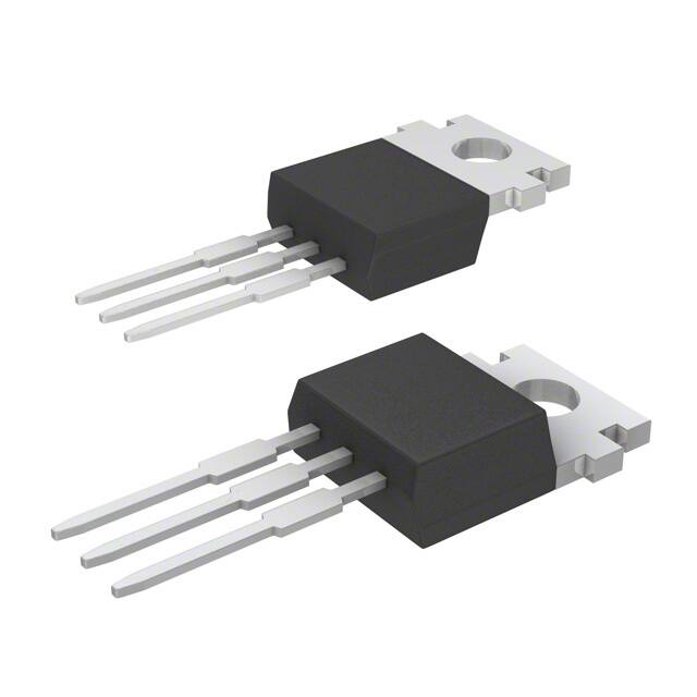
KCS (TO-220) PACKAGE
(TOP VIEW)
GND
OUT
GND
IN
Also designed for vehicular applications, the LM2940
and all regulated circuitry are protected from reverse
battery installations or two-battery jumps. During line
transients, such as load dump when the input
voltage can momentarily exceed the specified
maximum
operating
voltage,
the
regulator
automatically shuts down to protect both the internal
circuits and the load. The LM2940 is not harmed by
temporary mirror-image insertion. Familiar regulator
features, such as short-circuit and thermal-overload
protection, also are provided.
Please be aware that an important notice concerning availability, standard warranty, and use in critical applications of Texas
Instruments semiconductor products and disclaimers thereto appears at the end of this data sheet.
PRODUCTION DATA information is current as of publication date.
Products conform to specifications per the terms of the Texas
Instruments standard warranty. Production processing does not
necessarily include testing of all parameters.
Copyright © 2006, Texas Instruments Incorporated
�LM2940
1-A LOW-DROPOUT VOLTAGE REGULATOR
www.ti.com
SLVS634 – MAY 2006
ORDERING INFORMATION
TA
PACKAGE (1)
VZ
5V
0°C to 125°C
8V
12 V
5V
–40°C to 125°C
8V
12 V
(1)
ORDERABLE PART NUMBER
TOP-SIDE MARKING
SOT-223 (DCY)
Reel of 2500
LM2940-50CDCYR
PREVIEW
TO-220 (KCS)
Tube of 50
LM2940-50CKCSE3
LM2940-50C
TO-263 (KTT)
Reel of 1000
LM2940-50CKTTR
PREVIEW
SOT-223 (DCY)
Reel of 2500
LM2940-80CDCYR
PREVIEW
TO-220 (KCS)
Tube of 50
LM2940-80CKCS
PREVIEW
TO-263 (KTT)
Reel of 1000
LM2940-80CKTTR
PREVIEW
SOT-223 (DCY)
Reel of 2500
LM2940-120CDCYR
PREVIEW
TO-220 (KCS)
Tube of 50
LM2940-120CKCS
PREVIEW
TO-263 (KTT)
Reel of 1000
LM2940-120CKTTR
PREVIEW
SOT-223 (DCY)
Reel of 2500
LM2940-50IDCYR
PREVIEW
TO-220 (KCS)
Tube of 50
LM2940-50IKCSE3
LM2940-50I
TO-263 (KTT)
Reel of 1000
LM2940-50IKTTR
PREVIEW
SOT-223 (DCY)
Reel of 2500
LM2940-80IDCYR
PREVIEW
TO-220 (KCS)
Tube of 50
LM2940-80IKCS
PREVIEW
TO-263 (KTT)
Reel of 1000
LM2940-80IKTTR
PREVIEW
SOT-223 (DCY)
Reel of 2500
LM2940-120IDCYR
PREVIEW
TO-220 (KCS)
Tube of 50
LM2940-120IKCS
PREVIEW
TO-263 (KTT)
Reel of 1000
LM2940-120IKTTR
PREVIEW
Package drawings, standard packing quantities, thermal data, symbolization, and PCB design guidelines are available at
www.ti.com/sc/package.
SIMPLIFIED SCHEMATIC
VIN
X
4X
X
2 kW
350X
70X
.5X
.3X
2.5X
4X
X
.5X
VOUT
20 pF
4 pF
13 kW
15 kW
5.6 V
6 kW
19 kW
3 kW
2 kW
3X
X
100 W
50 W
3X
X
2.7 kW
4 kW
X
1.8 kW
2.4 kW
4X
2.4 kW
GND
2
Submit Documentation Feedback
�LM2940
1-A LOW-DROPOUT VOLTAGE REGULATOR
www.ti.com
SLVS634 – MAY 2006
Absolute Maximum Ratings
(1)
over free-air temperature range (unless otherwise noted)
VI
θJA
Input voltage range (2)
Package thermal impedance (3) (4)
TJ
Operating virtual junction temperature
Tstg
Storage temperature range
TL
(1)
(2)
(3)
(4)
MIN
MAX
–0.3
45
DCY package
52.8
KCS package
24.8
KTT package
25.3
–65
Maximum lead temperature, time for wave soldering
UNIT
V
°C/W
150
°C
150
°C
DCY package
4s
260
KCS package
10 s
260
KTT package
4s
245
°C
Stresses beyond those listed under Absolute Maximum Ratings may cause permanent damage to the device. These are stress ratings
only, and functional operation of the device at these or any other conditions beyond those indicated under Recommended Operating
Conditions is not implied. Exposure to absolute-maximum-rated conditions for extended periods may affect device reliability.
If load is returned to a negative power supply, the output must be diode clamped to GND.
Maximum power dissipation is a function of TJ(max), θJA, and TA. The maximum allowable power dissipation at any allowable ambient
temperature is PD = (TJ(max) – TA)/θJA. Operating at the absolute maximum TJ of 150°C can affect reliability.
The package thermal impedance is calculated in accordance with JESD 51-7.
Recommended Operating Conditions
MIN
VI
TA
Input voltage
Free-air temperature range
MAX
26
Commercial temperature
Extended temperature
Submit Documentation Feedback
0
125
–40
125
UNIT
V
°C
3
�LM2940
1-A LOW-DROPOUT VOLTAGE REGULATOR
www.ti.com
SLVS634 – MAY 2006
LM2940x Electrical Characteristics
VI = VO + 5 V, IO = 1 A, CO = 22 µF (unless otherwise noted)
PARAMETER
VO
TEST CONDITIONS
Output voltage
5 mA ≤ IO ≤ 1 A,
5 V: 6.25 V ≤ VI ≤ 26 V,
8 V: 9.4 V ≤ VI ≤ 26 V
Line regulation
VO + 2 V ≤ VI ≤ 26 V, IO = 5 mA
Load regulation
50 mA ≤ IO ≤ 1 A
LM2940I
LM2940C
ZO
Output impedance
IQ
Quiescent current
100 mAdc, 20 mArms, fO = 120 Hz
VO + 2 V ≤ VI ≤ 26 V,
IO = 5 mA
LM2940I
LM2940C
VI = VO + 5 V, IO = 1 A
Vn
Output noise
voltage
fO = 10 Hz to 100 kHz, IO = 5 mA
Ripple rejection
fO = 120 Hz, 1 Vrms,
IO = 100 mA
LM2940I
LM2940C
IO = 1 A
Dropout voltage
Reverse polarity
dc input voltage
IO = 500 mA
(1)
4
MIN
TYP
MAX
25°C
4.85
5
5.15
7.76
8
8.24
Full range
4.75
5.25
7.6
8.4
25°C
20
50
20
25°C
35
50
55
Full range
80
25°C
35
25°C
35
25°C
10
Full range
50
55
15
10
20
10
15
25°C
30
45
30
45
60
54
25°C
60
54
66
48
72
25°C
20
25°C
385
54
dB
66
500
385
800
250
RO = 100 Ω, t ≤ 1 ms
LM2940C
LM2940I
RO = 100 Ω
RO = 100 Ω,
t ≤ 100 ms
LM2940I
RO = 100 Ω, t ≤ 1 ms
LM2940C
500
800
300
mV
600
110
150
200
25°C
1.6
1.9
1.6
1.9
25°C
60
75
60
75
Full range
60
25°C
45
55
45
55
25°C
–15
–30
–15
–30
Full range
–15
25°C
–15
–30
–15
–30
–75
–50
–75
25°C
–50
Full range
–50
25°C
–45
Full range
–45
Full range TA is –40°C to 125°C for the LM2940I and 0°C to 125°C for the LM2940C.
Submit Documentation Feedback
mV/
1000 h
32
Full range
LM2940I
µVrms
240
72
mA
60
150
60
mV
15
15
25°C
mV
mΩ
10
Full range
V
80
25°C
25°C
UNIT
80
55
25°C
RO = 100 Ω,
t ≤ 100 ms
80
130
20
Full range
LM2940C
Reverse polarity
transient input
voltage
MAX
25°C
Short-circuit current
Maximum line
transient
8V
TYP
Full range
IO = 100 mA
IO(MAX)
5V
MIN
Full range
Long-term stability
VI – VO
TA (1)
60
V
–15
V
–50
–55
–50
–50
A
–50
V
�LM2940
1-A LOW-DROPOUT VOLTAGE REGULATOR
www.ti.com
SLVS634 – MAY 2006
LM2940x Electrical Characteristics
VI = VO + 5 V, IO = 1 A, CO = 22 µF (unless otherwise noted)
PARAMETER
VO
TEST CONDITIONS
Output voltage
5 mA ≤ IO ≤ 1 A,
9 V: 10.5 V ≤ VI ≤ 26 V,
12 V: 13.6 V ≤ VI ≤ 26 V
Line regulation
VO + 2 V ≤ VI ≤ 26 V, IO = 5 mA
Load regulation
50 mA ≤ IO ≤ 1 A
LM2940I
LM2940C
ZO
Output impedance
IQ
Quiescent current
100 mAdc, 20 mArms, fO = 120 Hz
VO + 2 V ≤ VI ≤ 26 V,
IO = 5 mA
LM2940I
LM2940C
VI = VO + 5 V, IO = 1 A
Vn
Output noise voltage
fO = 10 Hz to 100 kHz, IO = 5 mA
Ripple rejection
fO = 120 Hz, 1 Vrms,
IO = 100 mA
LM2940I
LM2940C
IO = 1 A
Dropout voltage
Reverse polarity
dc input voltage
LM2940I
RO = 100 Ω, t ≤ 1 ms
LM2940C
LM2940I
LM2940C
Reverse polarity transient input
voltage
(1)
RO = 100 Ω, t ≤ 100 ms
RO = 100 Ω, t ≤ 1 ms
25°C
11.64
12
12.36
Full range
11.4
12.6
25°C
20
120
25°C
55
120
Full range
200
25°C
55
25°C
80
25°C
10
Full range
LM2940I
LM2940C
UNIT
V
mV
mV
120
mΩ
15
20
25°C
10
15
25°C
30
45
mA
60
25°C
µVrms
360
25°C
54
Full range
48
25°C
54
66
dB
66
25°C
48
25°C
400
mV/
1000 h
500
800
110
Full range
RO = 100 Ω, t ≤ 100 ms
RO = 100 Ω
MAX
25°C
Short-circuit current
Maximum line transient
TYP
Full range
IO = 100 mA
IO(MAX)
12 V
MIN
Full range
Long-term stability
VI – VO
TA (1)
150
mV
200
25°C
1.6
1.9
25°C
60
75
Full range
60
25°C
45
55
25°C
–15
–30
Full range
–15
25°C
–15
–30
25°C
–50
–75
Full range
–50
25°C
–45
Full range
–45
A
V
V
–55
V
Full range TA is –40°C to 125°C for the LM2940I and 0°C to 125°C for the LM2940C.
Submit Documentation Feedback
5
�LM2940
1-A LOW-DROPOUT VOLTAGE REGULATOR
www.ti.com
SLVS634 – MAY 2006
TYPICAL CHARACTERISTICS
DROPOUT VOLTAGE
vs
OUTPUT CURRENT
DROPOUT VOLTAGE
vs
TEMPERATURE
600
500
550
(V I – V O) – Dropout Voltage – mV
(V I – V O) – Dropout Voltage – mV
450
400
350
300
250
200
150
100
500
450
400
IO = 1 A
350
300
250
200
150
IO = 100 mA
100
50
50
0
-40 -25 -10
0
0
0.1 0.2 0.3 0.4 0.5 0.6 0.7 0.8 0.9
1
OUTPUT VOLTAGE
vs
TEMPERATURE
40
IO = 5 mA
VI = VO + 5 V
35
VO = 5 V
IQ – Quiescent Current – mA
5.3
VO – Output Voltage – V
50 65 80 95 110 125
QUIESCENT CURRENT
vs
TEMPERATURE
5.5
5.2
5.1
5
4.9
4.8
4.7
30
25
4.5
-40 -25 -10 5
20 35 50 65 80 95 110 125
IO = 1 A
20
15
IO = 500 mA
10
5
4.6
IO = 10 mA
0
-40 -25 -10
TA – Temperature – °C
6
20 35
TA – Air Temperature – °C
IO – Output Current – A
5.4
5
5
20 35 50 65 80 95 110 125
TA – Temperature – °C
Submit Documentation Feedback
�LM2940
1-A LOW-DROPOUT VOLTAGE REGULATOR
www.ti.com
SLVS634 – MAY 2006
TYPICAL CHARACTERISTICS (continued)
QUIESCENT CURRENT
vs
INPUT VOLTAGE
QUIESCENT CURRENT
vs
LOAD CURRENT
100
40
VO = 5 V
VI = 10 V
VO = 5 V
35
TJ = 25°C
80
IQ – Quiescent Current – mA
70
60
IO = 1 A
50
40
IO = 500 mA
30
IO = 100 mA
20
30
25
20
15
10
5
10
0
0
0
5
10
15
20
25
0
0.1
VI – Input Voltage – V
VI = 10 V
16
14
IO = 0 mA
10
12
0
10
-10
8
-20
6
Input Voltage
-30
4
-40
2
-50
-40
0
-30
-20
-10
0
10
20
30
40
Output Voltage Deviation – V
VO = 5 V
Input Voltage Transient – V
Output Voltage Deviation – mV
0.5
0.4
0.3
18
Output Voltage
0.9
1
LOAD TRANSIENT RESPONSE
40
20
0.5 0.6 0.7 0.8
IL – Load Current – A
LINE TRANSIENT RESPONSE
30
0.2 0.3 0.4
VI = 10 V
VO = 5 V
0.2
0.1
0
-0.1
-0.2
Output Voltage
-0.3
-0.4
-0.5
-0.6
-0.7
Load Current
-0.8
-0.9
-1
0
CO = 22 µF
5.6
5.2
4.8
4.4
4
3.6
3.2
2.8
2.4
2
1.6
1.2
0.8
Load Current – A
IQ – Quiescent Current – mA
90
0.4
0
-0.4
10 20 30 40 50 60 70 80 90 100
t – Time – µs
t – Time – µs
Submit Documentation Feedback
7
�LM2940
1-A LOW-DROPOUT VOLTAGE REGULATOR
www.ti.com
SLVS634 – MAY 2006
TYPICAL CHARACTERISTICS (continued)
RIPPLE REJECTION
vs
FREQUENCY
LOW-VOLTAGE BEHAVIOR
OUTPUT VOLTAGE
vs
INPUT VOLTAGE
6
110
VI = 10 V
100
TJ = 25°C
Vripple = 1 Vrms
5
IO = 10 mA
80
VO – Output Voltage – V
Ripple Rejection – dB
90
70
60
50
IO = 100 mA
40
30
4
3.5
3
2.5
2
10
1.5
0
100
1k
1000
10k
10000
VO = 5 V
4.5
20
10
IO = 1 A
5.5
CO = 22 µF
1
100k
1M
100000
1000000
1
1.5
2
2.5
f – Frequency – Hz
OUTPUT AT VOLTAGE EXTREMES
OUTPUT VOLTAGE
vs
INPUT VOLTAGE
4.5
IO – Short-Circuit Current – A
VO – Output Voltage – V
7
6
5
4
3
2
1
0
4.5
5
5.5
6
VI – VO = 10 V
4
3.5
3
2.5
2
1.5
1
0.5
-1
-20
-10
0
10
20
30
40
0
-40 -25 -10
5
20
35 50
65 80 95 110 125
TA – Temperature – °C
VI – Input Voltage – V
8
4
5
RL = 100 Ω
VO = 5V
8
-2
-30
3.5
SHORT-CIRCUIT CURRENT
vs
TEMPERATURE
10
9
3
VI – Input Voltage – V
Submit Documentation Feedback
�LM2940
1-A LOW-DROPOUT VOLTAGE REGULATOR
www.ti.com
SLVS634 – MAY 2006
TYPICAL CHARACTERISTICS (continued)
OUTPUT IMPEDANCE
vs
FREQUENCY
10
VI = 10 V
ZO – Output Impedance – Ω
CO = 22 µF
IO = 10 mA
Vripple = 1 VPP
1
0.1
0.01
10
1.E+01
100
1.E+02
1k
1.E+03
10k
1.E+04
100k
1.E+05
1M
1.E+06
f – Frequency – Hz
Submit Documentation Feedback
9
�LM2940
1-A LOW-DROPOUT VOLTAGE REGULATOR
www.ti.com
SLVS634 – MAY 2006
APPLICATION INFORMATION
Typical Application
Figure 1 shows a typical circuit configuration for the LM2940.
VI
Unregulated Input
VO
Regulated Output
LM2940
C1
0.47 µF
(see Note A)
CO
22 µF
(see Note B)
IQ
A.
Required in regulator if located far from power-supply filter
B.
CO must be at least 22 µF to maintain stability. May be increased without bound to maintain regulation during
transients. Locate as close as possible to the regulator. This capacitor must be rated over the same operating
temperature range as the regulator, and proper ESR is critical.
Figure 1. Typical Application Circuit
External Capacitors
The output capacitor is critical to maintaining regulator stability and must meet the required conditions for both
equivalent series resistance (ESR) and minimum capacitance.
Minimum Capacitance
The minimum output capacitance required to maintain stability is 22 µF (this value may be increased without
limit). Larger values of output capacitance give improved transient response.
ESR Limits
The ESR of the output capacitor causes loop instability if it is too high or too low. The acceptable range of ESR
plotted versus load current is shown in Typical Characteristics. It is essential that the output capacitor meet
these requirements, or oscillations can result.
It is important to note that for most capacitors, ESR is specified only at room temperature. However, the
designer must ensure that the ESR stays inside the limits shown over the entire operating range for the design.
For aluminum electrolytic capacitors, ESR can increase by about 30 times as the temperature is reduced from
25°C to –40°C. This type of capacitor is not well suited for low-temperature operation.
Solid tantalum capacitors have a more stable ESR over temperature, but are more expensive than aluminum
electrolytics. A cost-effective approach sometimes used is to parallel an aluminum electrolytic with a solid
tantalum, with the total capacitance split about 75%/25% with the aluminum being the larger value.
ESR – Equivalent Series Resistance – Ω
If two capacitors are paralleled, the effective ESR is the parallel of the two individual values. The flatter ESR or
the tantalum keeps the effective ESR from rising as quickly at low temperatures.
100
CO = 22 µF
VO = 5 V
10
1
Stable Region
0.1
0.01
0
200
400
600
800
1000
IO – Output Current – mA
Figure 2. Output Capacitor ESR
10
Submit Documentation Feedback
�LM2940
1-A LOW-DROPOUT VOLTAGE REGULATOR
www.ti.com
SLVS634 – MAY 2006
APPLICATION INFORMATION (continued)
Heatsinking
A heatsink may be required, depending on the maximum power dissipation and maximum ambient temperature
of the application. Under all possible operating conditions, the junction temperature must be within the range
specified under absolute maximum ratings.
To determine if a heatsink is required, the power dissipated by the regulator, PD, must be calculated.
Figure 3 shows the voltages and currents that are present in the circuit, as well as the formula for calculating the
power dissipated in the regulator.
IIN
VIN
VOUT
IN
OUT
GND
IL
LOAD
IG
II = IL + IG
PD = (VIN – VOUT)IL + (VIN)IG
Figure 3. Power Dissipation
The next parameter that must be calculated is the maximum allowable temperature rise, TR(max). This is
calculated using the formula:
TR(max) = TJ(max) – TA(max)
Where
TJ(max) is the maximum allowable junction temperature, which is 125°C for commercial parts.
TA(max) is the maximum ambient temperature encountered in the application.
Using the calculated valued for TR(max) and PD, the maximum allowable value for the junction-to-ambient
thermal resistance, θJA, now can be found:
θJA = TR(max) ÷ PD
NOTE:
If the maximum allowable value for θJA is found to be ≥53°C/W for the TO-220
package, ≥80°C/W for the TO-263 package, or ≥174°C/W for the SOT-223 package,
no heatsink is needed, because the package alone dissipates enough heat to satisfy
these requirements.
If the calculated value for θJA falls below these limits, a heatsink is required.
Submit Documentation Feedback
11
�LM2940
1-A LOW-DROPOUT VOLTAGE REGULATOR
www.ti.com
SLVS634 – MAY 2006
APPLICATION INFORMATION (continued)
Heatsinking TO-220 Package Parts
The SOT-223 can be attached to a typical heatsink or secured to a copper plane on a PC board. If a copper
plane is use, the values of θJA are the same as shown in under Heatsinking TO-263 and SOT-223 Package
Parts.
If a manufactured heatsink is selected, the value of heatsink-to-ambient thermal resistance, θHA, must be
calculated:
θHA = θJA – θCH – θJC
Where
θJC is defined as the thermal resistance from the junction to the surface of the case. A value of 3°C/W can
be assumed for θJC for this calculation.
θCH is defined as the thermal resistance between the case and the surface of the heatsink. The value of θCH
varies from about 1.5°C/W to about 2.5°C/W, depending on the method of attachment, insulator, etc. If the
exact value is unknown, 2°C/W should be assumed for θCH.
Heatsinking TO-263 and SOT-223 Package Parts
Both the TO-263 and SOT-223 packages use a copper plane on the PCB and the PCB itself as a heatsink. To
optimize the heatsinking ability of the plane and PCB, solder the tab of the package to the plane.
qJA – Thermal Resistance – °C/W
Figure 4 shows the measured values of θJA for the TO-263 for different copper area sizes using a typical PCB
with 1-oz copper and no solder mask over the copper area used for heatsinking.
80
70
60
50
40
30
0
1
3
2
2
Copper Foil Area – in
Figure 4. θJA vs Copper (1 oz) Area for TO-263 Package
As shown in Figure 4, increasing the copper area beyond 1 in2 produces very little improvement. It should also
be observed that the minimum value of θJA for the TO-263 package mounted to a PCB is 32°C/W.
As a design aid, Figure 5 shows the maximum allowable power dissipation compared to ambient temperature for
the TO-263 device, assuming θJA is 35°C/W and the maximum junction temperature is 125°C.
12
Submit Documentation Feedback
�LM2940
1-A LOW-DROPOUT VOLTAGE REGULATOR
www.ti.com
SLVS634 – MAY 2006
PD – Maximum Power Dissipation – W
APPLICATION INFORMATION (continued)
5
4
3
2
TO-263 Package
PCB Mount
1-in2 Copper
1
0
-40
-25
75
25
125
TA – Ambient Temperature – °C
Figure 5. Maximum Power Dissipation vs Ambient Temperature for TO-263 Package
qJA – Thermal Resistance – °C/W
Figure 6 and Figure 7 show the information for the SOT-223 package. Figure 7 assumes a θJA of 74°C/W for
1-oz copper, 51°C/W for 2-oz copper, and a maximum junction temperature of 125°C.
200
170
140
110
80
50
0
1
3
2
2
Copper Foil Area – in
PD – Maximum Power Dissipation – W
Figure 6. θJA vs Copper (2 oz) Area for SOT-223 Package
5
4
SOT-223 Package
PCB Mount
2
1-in Copper
3
2-oz Copper
2
1
1-oz Copper
0
-40
-25
25
75
125
TA – Ambient Temperature – °C
Figure 7. Maximum Power Dissipation vs Ambient Temperature for SOT-223 Package
Submit Documentation Feedback
13
�PACKAGE OPTION ADDENDUM
www.ti.com
18-Jul-2006
PACKAGING INFORMATION
Orderable Device
Status (1)
Package
Type
Package
Drawing
Pins Package Eco Plan (2)
Qty
LM2940-50CKCSE3
ACTIVE
TO-220
KCS
3
50
Pb-Free
(RoHS)
CU SN
N / A for Pkg Type
LM2940-50IKCSE3
ACTIVE
TO-220
KCS
3
50
Pb-Free
(RoHS)
CU SN
N / A for Pkg Type
Lead/Ball Finish
MSL Peak Temp (3)
(1)
The marketing status values are defined as follows:
ACTIVE: Product device recommended for new designs.
LIFEBUY: TI has announced that the device will be discontinued, and a lifetime-buy period is in effect.
NRND: Not recommended for new designs. Device is in production to support existing customers, but TI does not recommend using this part in
a new design.
PREVIEW: Device has been announced but is not in production. Samples may or may not be available.
OBSOLETE: TI has discontinued the production of the device.
(2)
Eco Plan - The planned eco-friendly classification: Pb-Free (RoHS), Pb-Free (RoHS Exempt), or Green (RoHS & no Sb/Br) - please check
http://www.ti.com/productcontent for the latest availability information and additional product content details.
TBD: The Pb-Free/Green conversion plan has not been defined.
Pb-Free (RoHS): TI's terms "Lead-Free" or "Pb-Free" mean semiconductor products that are compatible with the current RoHS requirements
for all 6 substances, including the requirement that lead not exceed 0.1% by weight in homogeneous materials. Where designed to be soldered
at high temperatures, TI Pb-Free products are suitable for use in specified lead-free processes.
Pb-Free (RoHS Exempt): This component has a RoHS exemption for either 1) lead-based flip-chip solder bumps used between the die and
package, or 2) lead-based die adhesive used between the die and leadframe. The component is otherwise considered Pb-Free (RoHS
compatible) as defined above.
Green (RoHS & no Sb/Br): TI defines "Green" to mean Pb-Free (RoHS compatible), and free of Bromine (Br) and Antimony (Sb) based flame
retardants (Br or Sb do not exceed 0.1% by weight in homogeneous material)
(3)
MSL, Peak Temp. -- The Moisture Sensitivity Level rating according to the JEDEC industry standard classifications, and peak solder
temperature.
Important Information and Disclaimer:The information provided on this page represents TI's knowledge and belief as of the date that it is
provided. TI bases its knowledge and belief on information provided by third parties, and makes no representation or warranty as to the
accuracy of such information. Efforts are underway to better integrate information from third parties. TI has taken and continues to take
reasonable steps to provide representative and accurate information but may not have conducted destructive testing or chemical analysis on
incoming materials and chemicals. TI and TI suppliers consider certain information to be proprietary, and thus CAS numbers and other limited
information may not be available for release.
In no event shall TI's liability arising out of such information exceed the total purchase price of the TI part(s) at issue in this document sold by TI
to Customer on an annual basis.
Addendum-Page 1
��IMPORTANT NOTICE
Texas Instruments Incorporated and its subsidiaries (TI) reserve the right to make corrections, modifications,
enhancements, improvements, and other changes to its products and services at any time and to discontinue
any product or service without notice. Customers should obtain the latest relevant information before placing
orders and should verify that such information is current and complete. All products are sold subject to TI’s terms
and conditions of sale supplied at the time of order acknowledgment.
TI warrants performance of its hardware products to the specifications applicable at the time of sale in
accordance with TI’s standard warranty. Testing and other quality control techniques are used to the extent TI
deems necessary to support this warranty. Except where mandated by government requirements, testing of all
parameters of each product is not necessarily performed.
TI assumes no liability for applications assistance or customer product design. Customers are responsible for
their products and applications using TI components. To minimize the risks associated with customer products
and applications, customers should provide adequate design and operating safeguards.
TI does not warrant or represent that any license, either express or implied, is granted under any TI patent right,
copyright, mask work right, or other TI intellectual property right relating to any combination, machine, or process
in which TI products or services are used. Information published by TI regarding third-party products or services
does not constitute a license from TI to use such products or services or a warranty or endorsement thereof.
Use of such information may require a license from a third party under the patents or other intellectual property
of the third party, or a license from TI under the patents or other intellectual property of TI.
Reproduction of information in TI data books or data sheets is permissible only if reproduction is without
alteration and is accompanied by all associated warranties, conditions, limitations, and notices. Reproduction
of this information with alteration is an unfair and deceptive business practice. TI is not responsible or liable for
such altered documentation.
Resale of TI products or services with statements different from or beyond the parameters stated by TI for that
product or service voids all express and any implied warranties for the associated TI product or service and
is an unfair and deceptive business practice. TI is not responsible or liable for any such statements.
Following are URLs where you can obtain information on other Texas Instruments products and application
solutions:
Products
Applications
Amplifiers
amplifier.ti.com
Audio
www.ti.com/audio
Data Converters
dataconverter.ti.com
Automotive
www.ti.com/automotive
DSP
dsp.ti.com
Broadband
www.ti.com/broadband
Interface
interface.ti.com
Digital Control
www.ti.com/digitalcontrol
Logic
logic.ti.com
Military
www.ti.com/military
Power Mgmt
power.ti.com
Optical Networking
www.ti.com/opticalnetwork
Microcontrollers
microcontroller.ti.com
Security
www.ti.com/security
Low Power Wireless www.ti.com/lpw
Mailing Address:
Telephony
www.ti.com/telephony
Video & Imaging
www.ti.com/video
Wireless
www.ti.com/wireless
Texas Instruments
Post Office Box 655303 Dallas, Texas 75265
Copyright 2006, Texas Instruments Incorporated
�