Order
Now
Product
Folder
Support &
Community
Tools &
Software
Technical
Documents
LM2991
SNVS099I – MAY 1999 – REVISED OCTOBER 2016
LM2991 Negative Low-Dropout Adjustable Regulator
1 Features
•
1
•
•
•
•
•
•
•
3 Description
The LM2991 is a low dropout adjustable negative
regulator with a output voltage range between −3 V to
−24 V. The LM2991 provides up to 1 A of load
current and features a ON /OFF pin for remote
shutdown capability.
Output Voltage Adjustable from −3 V to −24 V,
Typically −2 V to −25 V
Output Current in Excess of 1 A
Dropout Voltage Typically 0.6 V at 1-A Load
Low Quiescent Current
Internal Short Circuit Current Limit
Internal Thermal Shutdown With Hysteresis
TTL, CMOS Compatible ON/OFF Switch
Functional Complement to the LM2941 Series
The LM2991 uses new circuit design techniques to
provide a low dropout voltage, low quiescent current
and low temperature coefficient precision reference.
The dropout voltage at 1-A load current is typically
0.6 V and an ensured worst-case maximum of 1 V
over the entire operating temperature range. The
quiescent current is typically 1 mA with a 1-A load
current and an input-output voltage differential greater
than 3 V. A unique circuit design of the internal bias
supply limits the quiescent current to only 9 mA
(typical) when the regulator is in the dropout mode
(VOUT − VIN ≤ 3 V).
2 Applications
•
•
•
•
•
Post Switcher Regulator
Local, On-Card, Regulation
Battery Operated Equipment
Industrial
Instrumentation
The LM2991 is short-circuit proof, and thermal
shutdown includes hysteresis to enhance the
reliability of the device when inadvertently overloaded
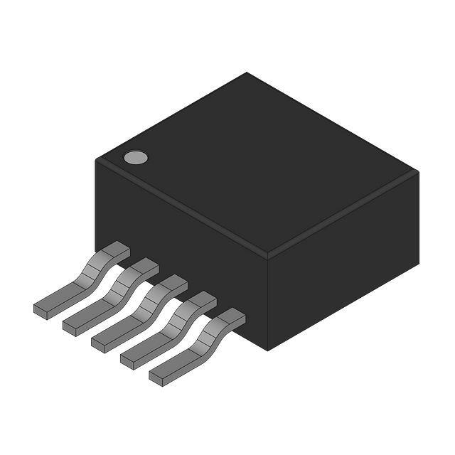
for extended periods. The LM2991 is available in 5lead TO-220 and DDPAK/TO-263 packages and is
rated for operation over the automotive temperature
range of −40°C to +125°C. Mil-Aero versions are also
available.
Device Information(1)
PART NUMBER
LM2991
PACKAGE
BODY SIZE (NOM)
DDPAK/TO-263 (5)
10.20 mm × 9.00 mm
TO-220 (5)
14.99 mm × 10.16 mm
(1) For all available packages, see the orderable addendum at
the end of the data sheet.
Typical Application
GND
R1
+
+
CIN*
COUT**
ADJ
Unregulated
Input
IN
LM2991
OUT
R2
Regulated
Input
ON/OFF
Copyright © 2016, Texas Instruments Incorporated
VOUT = VREF (1 + R2/R1)
* Required if the regulator is located further than 6 inches from the power supply filter capacitors. A 1-μF solid
tantalum or a 10-μF aluminum electrolytic capacitor is recommended.
** Required for stability. Must be at least a 10-μF aluminum electrolytic or a 1-μF solid tantalum to maintain stability.
May be increased without bound to maintain regulation during transients. Locate the capacitor as close as possible to
the regulator. The equivalent series resistance (ESR) is critical, and should be less than 10Ω over the same operating
temperature range as the regulator.
1
An IMPORTANT NOTICE at the end of this data sheet addresses availability, warranty, changes, use in safety-critical applications,
intellectual property matters and other important disclaimers. PRODUCTION DATA.
�LM2991
SNVS099I – MAY 1999 – REVISED OCTOBER 2016
www.ti.com
Table of Contents
1
2
3
4
5
6
7
Features ..................................................................
Applications ...........................................................
Description .............................................................
Revision History.....................................................
Pin Configuration and Functions .........................
Specifications.........................................................
1
1
1
2
3
4
6.1
6.2
6.3
6.4
6.5
6.6
4
4
4
4
5
6
Absolute Maximum Ratings ......................................
ESD Ratings..............................................................
Recommended Operating Conditions.......................
Thermal Information ..................................................
Electrical Characteristics...........................................
Typical Characteristics ..............................................
Detailed Description .............................................. 9
7.1
7.2
7.3
7.4
Overview ................................................................... 9
Functional Block Diagram ......................................... 9
Feature Description................................................... 9
Device Functional Modes........................................ 10
8
Application and Implementation ........................ 11
8.1 Application Information............................................ 11
8.2 Typical Application ................................................. 11
9 Power Supply Recommendations...................... 15
10 Layout................................................................... 16
10.1 Layout Guidelines ................................................. 16
10.2 Layout Example .................................................... 16
11 Device and Documentation Support ................. 17
11.1
11.2
11.3
11.4
11.5
11.6
11.7
Device Support ....................................................
Related Documentation .......................................
Receiving Notification of Documentation Updates
Community Resources..........................................
Trademarks ...........................................................
Electrostatic Discharge Caution ............................
Glossary ................................................................
17
17
17
17
17
18
18
12 Mechanical, Packaging, and Orderable
Information ........................................................... 18
4 Revision History
NOTE: Page numbers for previous revisions may differ from page numbers in the current version.
Changes from Revision H (June 2013) to Revision I
Page
•
Added Device Information and ESD Rating tables, Feature Description, Device Functional Modes, Application and
Implementation, Power Supply Recommendations, Layout, Device and Documentation Support, and Mechanical,
Packaging, and Orderable Information sections; moved some curves to Application Curves section .................................. 1
•
Changed footnote 4 of Abs Max table and footnote 1 to Typical Characteristics to eliminate obsolete thermal values
for thetaJA; updated values are in Thermal Information ....................................................................................................... 4
•
Changed Figure 14 as previous thermal values have been updated .................................................................................... 8
Changes from Revision G (April 2013) to Revision H
•
2
Page
Changed layout of National Semiconductor data sheet to TI format...................................................................................... 1
Submit Documentation Feedback
Copyright © 1999–2016, Texas Instruments Incorporated
Product Folder Links: LM2991
�LM2991
www.ti.com
SNVS099I – MAY 1999 – REVISED OCTOBER 2016
5 Pin Configuration and Functions
KC and NDH Packages
5-Pin TO-220
Top View
KTT Package
5-Pin DDPAK/TO-263
Top View
5 OUT
Input
4 GND
3 IN
Tab is input
5
OUT
4
GND
2 ON/OFF
3
IN
1 ADJ
2
ON/OFF
1
ADJ
Pin Functions
PIN
NO.
NAME
I/O
DESCRIPTION
1
ADJ
I
Feedback pin to the control loop for programming the output voltage.
2
ON/OFF
I
Logic high enable input
3
IN
I
Negative Input voltage. Internally connected directly to the thermal
tab.
4
GND
—
Ground
5
OUT
O
Regulated output voltage
I
Negative Input voltage. Internally connected directly to the device pin
3. The thermal tab must be connected to a copper area on the PCB
at the same potential as device pin 3 (IN) to assure thermal
performance, or leave the thermal tab floating. Do NOT connect the
thermal tab to any potential other than the same potential at device
pin 3. Do NOT connect the thermal tab to ground.
—
TAB
Submit Documentation Feedback
Copyright © 1999–2016, Texas Instruments Incorporated
Product Folder Links: LM2991
3
�LM2991
SNVS099I – MAY 1999 – REVISED OCTOBER 2016
www.ti.com
6 Specifications
6.1 Absolute Maximum Ratings
over operating free-air temperature range (unless otherwise noted) (1) (2)
Input voltage
Power dissipation
(2)
(3)
MAX
UNIT
–26
0.3
V
(3)
Internally limited
Storage temperature, Tstg
(1)
MIN
–65
150
°C
Stresses beyond those listed under Absolute Maximum Ratings may cause permanent damage to the device. These are stress ratings
only, which do not imply functional operation of the device at these or any other conditions beyond those indicated under Recommended
Operating Conditions. Exposure to absolute-maximum-rated conditions for extended periods may affect device reliability.
If Military/Aerospace specified devices are required, contact the Texas Instruments Sales Office/Distributors for availability and
specifications.
The maximum power dissipation is a function of TJ(MAX), RθJA, and TA. The maximum allowable power dissipation at any ambient
temperature is PD = (TJ(MAX) − TA)/RθJA. If this dissipation is exceeded, the die temperature will rise above 125°C, and the LM2991 will
eventually go into thermal shutdown at a TJ of approximately 160°C. Refer to Thermal Shutdown for more details.
6.2 ESD Ratings
V(ESD)
(1)
Electrostatic discharge
Human-body model (HBM), per ANSI/ESDA/JEDEC JS-001 (1)
VALUE
UNIT
±2000
V
JEDEC document JEP155 states that 500-V HBM allows safe manufacturing with a standard ESD control process.
6.3 Recommended Operating Conditions
over operating free-air temperature range (unless otherwise noted) (1)
MIN
Junction temperature, TJ
ON/OFF pin
Maximum input voltage (operational)
(1)
MAX
UNIT
–40
NOM
125
°C
0
5
V
–26
V
Stresses beyond those listed under Absolute Maximum Ratings may cause permanent damage to the device. These are stress ratings
only, which do not imply functional operation of the device at these or any other conditions beyond those indicated under Recommended
Operating Conditions. Exposure to absolute-maximum-rated conditions for extended periods may affect device reliability.
6.4 Thermal Information
LM2991
THERMAL METRIC (1)
TO-263 (KTT)
TO-220 (NDH) (2)
TO-220 (KC) (2)
5 PINS
5 PINS
5 PINS
UNIT
RθJA (3)
Junction-to-ambient thermal resistance, High-K
27.8
54.4
56.4
°C/W
RθJC(top)
Junction-to-case (top) thermal resistance
41.4
30.1
40.0
°C/W
RθJB
Junction-to-board thermal resistance
10.9
33.2
38.6
°C/W
ψJT
Junction-to-top characterization parameter
6.0
11.6
12.8
°C/W
ψJB
Junction-to-board characterization parameter
10.6
36.2
35.3
°C/W
RθJC(bot)
Junction-to-case (bottom) thermal resistance
0.7
0.5
0.6
°C/W
(1)
(2)
(3)
4
For more information about traditional and new thermal metrics, see Semiconductor and IC Package Thermal Metrics.
The TO-220 package is vertically mounted in center of a JEDEC High-K test board (JESD 51-7) with no additional heat sink attached.
This is a through-hole package; this is NOT a surface-mount package.
Thermal resistance value RθJA is based on the EIA/JEDEC High-K printed circuit board defined by JESD51-7 - High Effective Thermal
Conductivity Test Board for Leaded Surface Mount Packages.
Submit Documentation Feedback
Copyright © 1999–2016, Texas Instruments Incorporated
Product Folder Links: LM2991
�LM2991
www.ti.com
SNVS099I – MAY 1999 – REVISED OCTOBER 2016
6.5 Electrical Characteristics
VIN = −10 V, VOUT = −3 V, IOUT = 1 A, COUT = 47 μF, R1 = 2.7 kΩ, TJ = 25°C, unless otherwise specified.
PARAMETER
5 mA ≤ IOUT ≤ 1 A
Reference voltage
Output voltage (VOUT)
MIN
TYP (1)
MAX
–1.234
–1.210
–1.186
V
–1.15
V
–3
V
TEST CONDITIONS
5 mA ≤ IOUT ≤ 1 A, VOUT – 1 V ≥ VIN > −26 V
−40°C ≤ TJ ≤ 125°C
–1.27
–2
VIN = −26 V
–24
Line regulation
IOUT = 5 mA, VOUT −1 V > VIN > −26 V
Load regulation
50 mA ≤ IOUT ≤ 1 A
IOUT = 0.1 A, ΔVOUT ≤ 100 mV
Dropout voltage
–25
0.04
0.04%
0.4%
0.1
0.2
IOUT = 0.1 A, ΔVOUT ≤ 100 mV
−40°C ≤ TJ ≤ 125°C
IOUT = 1 A, ΔVOUT ≤ 100 mV
0.6
IOUT ≤ 1 A
0.8
0.7
IOUT = 1 A, −40°C ≤ TJ ≤ 125°C
5
Ripple rejection
Vripple = 1 VRMS,
ƒripple = 1 kHz, IOUT = 5 mA
Output noise
10 Hz to 100 kHz, IOUT = 5 mA
200
VOUT: ON
1.2
16
50
V
50
mA
mA
60
VOUT: ON −40°C ≤ TJ ≤ 125°C
dB
450
µV
V
0.8
VOUT: OFF
1.3
VOUT: OFF, −40°C ≤ TJ ≤ 125°C
V
2.4
VON/OFF = 0.8 V, VOUT: ON
0.1
10
VON/OFF = 2.4 V, VOUT: OFF
40
100
60
250
Output leakage current
VIN = −26 V, VON/OFF = 2.4 V, VOUT = 0 V
Current limit
VOUT = 0 V
(1)
V
1
VIN = VOUT, IOUT ≤ 1 A
ON/OFF input current
%/V
0.3
Dropout quiescent
current
ON/OFF input voltage
V
0.004
IOUT = 1 A, ΔVOUT ≤ 100 mV
−40°C ≤ TJ ≤ 125°C
Quiescent current
UNIT
1.5
µA
µA
2
A
Typicals are at TJ = 25°C and represent the most likely parametric norm.
Submit Documentation Feedback
Copyright © 1999–2016, Texas Instruments Incorporated
Product Folder Links: LM2991
5
�LM2991
SNVS099I – MAY 1999 – REVISED OCTOBER 2016
www.ti.com
6.6 Typical Characteristics
6
Figure 1. Dropout Voltage
Figure 2. Normalized Output Voltage
Figure 3. Output Voltage
Figure 4. Output Noise Voltage
Figure 5. Quiescent Current
Figure 6. Maximum Output Current
Submit Documentation Feedback
Copyright © 1999–2016, Texas Instruments Incorporated
Product Folder Links: LM2991
�LM2991
www.ti.com
SNVS099I – MAY 1999 – REVISED OCTOBER 2016
Typical Characteristics (continued)
Figure 7. Maximum Output Current
Figure 8. Ripple Rejection
Figure 9. Output Impedance
Figure 10. ON/OFF Control Voltage
Figure 12. Low Voltage Behavior
Figure 11. Adjust Pin Current
Submit Documentation Feedback
Copyright © 1999–2016, Texas Instruments Incorporated
Product Folder Links: LM2991
7
�LM2991
SNVS099I – MAY 1999 – REVISED OCTOBER 2016
www.ti.com
Typical Characteristics (continued)
5
4.5
Power Dissipation (W)
4
3.5
3
2.5
2
1.5
1
0.5
0
0
Figure 13. Maximum Power Dissipation (TO-220)
8
10
20
30
40
50
60
70
80
Ambient Temperature, TA (qC)
90
100
D001
Figure 14. Maximum Power Dissipation (DDPAK/TO-263)
Submit Documentation Feedback
Copyright © 1999–2016, Texas Instruments Incorporated
Product Folder Links: LM2991
�LM2991
www.ti.com
SNVS099I – MAY 1999 – REVISED OCTOBER 2016
7 Detailed Description
7.1 Overview
The LM2991 is a five-pin, low-dropout, 1-A negative adjustable voltage regulator and negative power supply,
ideally suited for a dual-supply system when using together with LM2941 series. The device may also be used as
an adjustable current-sink load.
7.2 Functional Block Diagram
7.3 Feature Description
7.3.1 ON/Off Pin
The LM2991 regulator can be turned off by applying a TTL or CMOS level high signal to the ON/OFF pin. The
impedance of the voltage source driving the ON/OFF pin must be low enough to source the ON/OFF pin input
current to meet the OFF threshold voltage level, 100 µA maximum at 2.4 V.
If the ON/OFF function is not needed, connect the pin to GND. The ON/OFF pin should not be left floating, as
this is not an ensured operating condition. See Figure 15.
7.3.2 Forcing The Output Positive
Due to an internal clamp circuit, the LM2991 can withstand positive voltages on its output. If the voltage source
pulling the output positive is DC, the current must be limited to 1.5 A. A current over 1.5 A fed back into the
LM2991 could damage the device. The LM2991 output can also withstand fast positive voltage transients up to
26 V, without any current limiting of the source. However, if the transients have a duration of over 1 ms, the
output should be clamped with a Schottky diode to ground.
7.3.3 Thermal Shutdown
The LM2991 has an internally set thermal shutdown point of typically 160°C, with approximately 10°C of
hysteresis. This thermal shutdown temperature point is outside the specified Recommended Operating
Conditions range, above the Absolute Maximum Ratings, and is intended as a safety feature for momentary fault
conditions only. Avoid continuous operation near the thermal shutdown temperature as it may have a negative
affect on the life of the device.
Submit Documentation Feedback
Copyright © 1999–2016, Texas Instruments Incorporated
Product Folder Links: LM2991
9
�LM2991
SNVS099I – MAY 1999 – REVISED OCTOBER 2016
www.ti.com
7.4 Device Functional Modes
7.4.1 Operation with VOUT(TARGET) –5 V ≥ VIN > –26 V
The device operates if the input voltage is within VOUT(TARGET) –5 V to –26 V range. At input voltages beyond the
VIN requirement, the devices do not operate correctly, and output voltage may not reach target value.
10
Submit Documentation Feedback
Copyright © 1999–2016, Texas Instruments Incorporated
Product Folder Links: LM2991
�LM2991
www.ti.com
SNVS099I – MAY 1999 – REVISED OCTOBER 2016
8 Application and Implementation
NOTE
Information in the following applications sections is not part of the TI component
specification, and TI does not warrant its accuracy or completeness. TI’s customers are
responsible for determining suitability of components for their purposes. Customers should
validate and test their design implementation to confirm system functionality.
8.1 Application Information
The LM2991 is a 1-A negative adjustable voltage regulator with an operating VIN range of –6 V to –26 V, and a
regulated VOUT having 5% accuracy with a maximum rated IOUT current of 1 A. Efficiency is defined by the ratio of
output voltage to input voltage because the LM2991 is a linear voltage regulator. To achieve high efficiency, the
dropout voltage (VIN – VOUT) must be as small as possible, thus requiring a very low dropout LDO.
Successfully implementing an LDO in an application depends on the application requirements. If the
requirements are simply input voltage and output voltage, compliance specifications (such as internal power
dissipation or stability) must be verified to ensure a solid design. If timing, start-up, noise, PSRR, or any other
transient specification is required, the design becomes more challenging.
8.2 Typical Application
Figure 15. LM2991 Typical Application With Adjustable Current Sink
8.2.1 Design Requirements
For this design example, use the parameters listed in Table 1 as the input parameters.
Table 1. Design Parameters
DESIGN PARAMETER
DESIGN REQUIREMENT
Input voltage
–26 V to –5 V
Output voltage
–2 V to –25 V (typical)
Output current
up to 1 A
Submit Documentation Feedback
Copyright © 1999–2016, Texas Instruments Incorporated
Product Folder Links: LM2991
11
�LM2991
SNVS099I – MAY 1999 – REVISED OCTOBER 2016
www.ti.com
8.2.2 Detailed Design Procedure
At 400-mA loading, the dropout of the LM2991 has 1-V maximum dropout over temperature, thus an –5 V
headroom is sufficient for operation over both input and output voltage accuracy. The efficiency of the LM2991 in
this configuration is VOUT / VIN = 50%.
To achieve the smallest form factor, the TO-263 (KTT) package is selected. Select input and output capacitors in
accordance with the External Capacitors section. Aluminum capacitances of 470 μF for the input and 50-μF
capacitors for the output are selected. With an efficiency of 50% and a 400-mA maximum load, the internal
power dissipation is 2000 mW, which corresponds to 82.5°C junction temperature rise for the TO-263 package.
With an 25°C ambient temperature, the junction temperature is at 107.5°C.
8.2.2.1 External Capacitors
The LM2991 regulator requires an output capacitor to maintain stability. The capacitor must be at least 10-μF
aluminum electrolytic or 1-μF solid tantalum. The equivalent series resistance (ESR) of the output capacitor must
be less than 10 Ω, or the zero added to the regulator frequency response by the ESR could reduce the phase
margin, creating oscillations. An input capacitor, of at least 1-μF solid tantalum or 10-μF aluminum electrolytic, is
also needed if the regulator is situated more than 6 inches from the input power supply filter.
8.2.2.1.1 Input Capacitor
TI recommends a solid tantalum or ceramic capacitor whose value is at least 1 μF, but an aluminum electrolytic
(≥ 10 μF) may be used. However, aluminum electrolytic types should not be used in applications where the
ambient temperature can drop below 0°C because their internal impedance increases significantly at cold
temperatures.
8.2.2.1.2 Output Capacitor
The output capacitor must meet the ESR limits shown in Figure 16, which means it must have an ESR between
about 25 mΩ and 10 Ω.
Figure 16. Output Capacitor ESR Range
A solid tantalum (value ≥ 1 µF) is the best choice for the output capacitor. An aluminum electrolytic (≥ 10 µF)
may be used if the ESR is in the stable range.
It should be noted that the ESR of a typical aluminum electrolytic will increase by as much as 50× as the
temperature is reduced from 25°C down to −40°C, while a tantalum exhibits an ESR increase of about 2× over
the same range. For this and other reasons, aluminum electrolytics should not be used in applications where low
operating temperatures occur.
The lower stable ESR limit of 25 mΩ means that ceramic capacitors can not be used directly on the output of an
LDO. A ceramic (≥ 2.2 µF) can be used on the output if some external resistance is placed in series with it (1 Ω
recommended). Dielectric types X7R or X5R must be used if the temperature range of the application varies
more than ± 25° from ambient to assure the amount of capacitance is sufficient.
12
Submit Documentation Feedback
Copyright © 1999–2016, Texas Instruments Incorporated
Product Folder Links: LM2991
�LM2991
www.ti.com
SNVS099I – MAY 1999 – REVISED OCTOBER 2016
8.2.2.2 Ceramic Bypass Capacitors
Many designers place distributed ceramic capacitors whose value is in the range of 1000 pF to 0.1 µF at the
power input pins of the IC's across a circuit board. These can cause reduced phase margin or oscillations in LDO
regulators.
The advent of multi-layer boards with dedicated power and ground planes has removed the trace inductance that
(previously) provided the necessary "de-coupling" to shield the output of the LDO from the effects of bypass
capacitors.
Avoid these capacitors, if possible; if ceramic bypass capacitors are used, keep them as far away from the LDO
output as is practical.
8.2.2.3 Minimum Load
A minimum load current of 500 μA is required for proper operation. The external resistor divider can provide the
minimum load, with the resistor from the adjust pin to ground set to 2.4 kΩ.
8.2.2.4 Setting The Output Voltage
The output voltage of the LM2991 is set externally by a resistor divider using Equation 1:
VOUT = VREF × (1 + R2/R1) − (IADJ × R2)
where
•
VREF = −1.21 V
(1)
The output voltage can be programmed within the range of −3 V to −24 V, typically an even greater range of −2
V to −25 V. The adjust pin current is about 60 nA, causing a slight error in the output voltage. However, using
resistors lower than 100 kΩ makes the error due to the adjust pin current negligible. For example, neglecting the
adjust pin current, and setting R2 to 100 kΩ and VOUT to −5 V, results in an output voltage error of only 0.16%.
8.2.2.5 Power Dissipation
Knowing the device power dissipation and proper sizing of the thermal plane connected to the thermal tab is
critical to ensuring reliable operation. Device power dissipation depends on input voltage, output voltage, and
load conditions and can be calculated with Equation 2.
PD(MAX) = (VIN(MAX) – VOUT) × IOUT
(2)
Power dissipation can be minimized, and greater efficiency can be achieved, by using the lowest available
voltage drop option that would still be greater than the dropout voltage (VDO). However, keep in mind that higher
voltage drops result in better dynamic (that is, PSRR and transient) performance.
Power dissipation and junction temperature are most often related by the junction-to-ambient thermal resistance
(RθJA) of the combined PCB and device package and the temperature of the ambient air (TA), according to
Equation 3 or Equation 4:
TJ(MAX) = TA(MAX) + (RθJA × PD(MAX))
PD(MAX) = (TJ(MAX) – TA(MAX)) / RθJA
(3)
(4)
Unfortunately, this RθJA is highly dependent on the heat-spreading capability of the particular PCB design, and
therefore varies according to the total copper area, copper weight, and location of the planes. The RθJA recorded
in Thermal Information is determined by the specific EIA/JEDEC JESD51-7 standard for PCB and copperspreading area, and is to be used only as a relative measure of package thermal performance. For a welldesigned thermal layout, RθJA is actually the sum of the package junction-to-case (bottom) thermal resistance
(RθJCbot) plus the thermal resistance contribution by the PCB copper area acting as a heat sink.
Submit Documentation Feedback
Copyright © 1999–2016, Texas Instruments Incorporated
Product Folder Links: LM2991
13
�LM2991
SNVS099I – MAY 1999 – REVISED OCTOBER 2016
www.ti.com
8.2.2.6 Estimating Junction Temperature
The EIA/JEDEC standard recommends the use of psi (Ψ) thermal characteristics to estimate the junction
temperatures of surface mount devices on a typical PCB board application. These characteristics are not true
thermal resistance values, but rather package specific thermal characteristics that offer practical and relative
means of estimating junction temperatures. These psi metrics are determined to be significantly independent of
copper-spreading area. The key thermal characteristics (ΨJT and ΨJB) are given in Thermal Information and are
used in accordance with Equation 5 or Equation 6.
TJ(MAX) = TTOP + (ΨJT × PD(MAX))
where
•
•
PD(MAX) is explained in Equation 4
TTOP is the temperature measured at the center-top of the device package.
TJ(MAX) = TBOARD + (ΨJB × PD(MAX))
(5)
where
•
•
PD(MAX) is explained in Equation 4
TBOARD is the PCB surface temperature measured 1-mm from the device package and centered on the
package edge.
(6)
For more information about the thermal characteristics ΨJT and ΨJB, see Semiconductor and IC Package Thermal
Metrics; for more information about measuring TTOP and TBOARD, see Using New Thermal Metrics; and for more
information about the EIA/JEDEC JESD51 PCB used for validating RθJA, see Thermal Characteristics of Linear
and Logic Packages Using JEDEC PCB Designs. These application notes are available at www.ti.com..
8.2.3 Application Curves
Figure 17. Line Transient Response
14
Submit Documentation Feedback
Figure 18. Load Transient Response
Copyright © 1999–2016, Texas Instruments Incorporated
Product Folder Links: LM2991
�LM2991
www.ti.com
SNVS099I – MAY 1999 – REVISED OCTOBER 2016
8.2.4 Additional Application Circuits
Figure 19. Fully Isolated Post-Switcher Regulator
9 Power Supply Recommendations
The LM2991 is designed to operate from an input voltage supply range between –6 V and –26 V. The input
voltage range must provide adequate headroom in order for the device to have a regulated output. This input
supply must be well regulated.
Submit Documentation Feedback
Copyright © 1999–2016, Texas Instruments Incorporated
Product Folder Links: LM2991
15
�LM2991
SNVS099I – MAY 1999 – REVISED OCTOBER 2016
www.ti.com
10 Layout
10.1 Layout Guidelines
The dynamic performance of the LM2991 is dependent on the layout of the PCB. PCB layout practices that are
adequate for typical LDOs may degrade the PSRR, noise, or transient performance of the device. Best
performance is achieved by placing CIN and COUT on the same side of the PCB as the LM2991, and as close as
is practical to the package. The ground connections for CIN and COUT must be back to the LM2991 GND pin
using as wide and short of a copper trace as is practical.
Good PC layout practices must be used or instability can be induced because of ground loops and voltage drops.
The input and output capacitors must be directly connected to the IN, OUT, and GND pins of the LM2991 using
traces which do not have other currents flowing in them (Kelvin connect). The best way to do this is to lay out CIN
and COUT near the device with short traces to the IN, OUT, and GND pins. The regulator ground pin must be
connected to the external circuit ground so that the regulator and its capacitors have a single-point ground.
Stability problems have been seen in applications where vias to an internal ground plane were used at the
ground points of the LM2991 device and the input and output capacitors. This was caused by varying ground
potentials at these nodes resulting from current flowing through the ground plane. Using a single point ground
technique for the regulator and its capacitors fixed the problem.
Because high current flows through the traces going into the IN pin and coming from the OUT pin, Kelvin connect
the capacitor leads to these pins so there is no voltage drop in series with the input and output capacitors.
10.2 Layout Example
Thermal
Vias
R1
ADJ
ON/OFF
IN
GND
OUT
VIN
1
2
3
4
5
CIN
R2
COUT VOUT
ON/OFF
GND
GND
Figure 20. LM2991 TO-263 Board Layout
16
Submit Documentation Feedback
Copyright © 1999–2016, Texas Instruments Incorporated
Product Folder Links: LM2991
�LM2991
www.ti.com
SNVS099I – MAY 1999 – REVISED OCTOBER 2016
11 Device and Documentation Support
11.1 Device Support
11.1.1 Device Nomenclature
Dropout Voltage: The input-output voltage differential at which the circuit ceases to regulate against further
reduction in input voltage. Measured when the output voltage has dropped 100 mV from the
nominal value obtained at (VOUT + 5 V) input, dropout voltage is dependent upon load current and
junction temperature.
Input Voltage: The DC voltage applied to the input terminals with respect to ground.
Input-Output Differential: The voltage difference between the unregulated input voltage and the regulated
output voltage for which the regulator will operate.
Line Regulation: The change in output voltage for a change in the input voltage. The measurement is made
under conditions of low dissipation or by using pulse techniques such that the average chip
temperature is not significantly affected.
Load Regulation: The change in output voltage for a change in load current at constant chip temperature.
Long Term Stability: Output voltage stability under accelerated life-test conditions after 1000 hours with
maximum rated voltage and junction temperature.
Output Noise Voltage: The rms AC voltage at the output, with constant load and no input ripple, measured over
a specified frequency range.
Quiescent Current: That part of the positive input current that does not contribute to the positive load current.
The regulator ground lead current.
Ripple Rejection: The ratio of the peak-to-peak input ripple voltage to the peak-to-peak output ripple voltage.
Temperature Stability of VOUT: The percentage change in output voltage for a thermal variation from room
temperature to either temperature extreme.
11.2 Related Documentation
For additional information, see the following:
• Semiconductor and IC Package Thermal Metrics
• Using New Thermal Metrics
• Thermal Characteristics of Linear and Logic Packages Using JEDEC PCB Designs
11.3 Receiving Notification of Documentation Updates
To receive notification of documentation updates, navigate to the device product folder on ti.com. In the upper
right corner, click on Alert me to register and receive a weekly digest of any product information that has
changed. For change details, review the revision history included in any revised document.
11.4 Community Resources
The following links connect to TI community resources. Linked contents are provided "AS IS" by the respective
contributors. They do not constitute TI specifications and do not necessarily reflect TI's views; see TI's Terms of
Use.
TI E2E™ Online Community TI's Engineer-to-Engineer (E2E) Community. Created to foster collaboration
among engineers. At e2e.ti.com, you can ask questions, share knowledge, explore ideas and help
solve problems with fellow engineers.
Design Support TI's Design Support Quickly find helpful E2E forums along with design support tools and
contact information for technical support.
11.5 Trademarks
E2E is a trademark of Texas Instruments.
Submit Documentation Feedback
Copyright © 1999–2016, Texas Instruments Incorporated
Product Folder Links: LM2991
17
�LM2991
SNVS099I – MAY 1999 – REVISED OCTOBER 2016
www.ti.com
11.5 Trademarks (continued)
All other trademarks are the property of their respective owners.
11.6 Electrostatic Discharge Caution
These devices have limited built-in ESD protection. The leads should be shorted together or the device placed in conductive foam
during storage or handling to prevent electrostatic damage to the MOS gates.
11.7 Glossary
SLYZ022 — TI Glossary.
This glossary lists and explains terms, acronyms, and definitions.
12 Mechanical, Packaging, and Orderable Information
The following pages include mechanical, packaging, and orderable information. This information is the most
current data available for the designated devices. This data is subject to change without notice and revision of
this document. For browser-based versions of this data sheet, refer to the left-hand navigation.
18
Submit Documentation Feedback
Copyright © 1999–2016, Texas Instruments Incorporated
Product Folder Links: LM2991
�PACKAGE OPTION ADDENDUM
www.ti.com
30-Sep-2021
PACKAGING INFORMATION
Orderable Device
Status
(1)
Package Type Package Pins Package
Drawing
Qty
Eco Plan
(2)
Lead finish/
Ball material
MSL Peak Temp
Op Temp (°C)
Device Marking
(3)
(4/5)
(6)
LM2991S
NRND
DDPAK/
TO-263
KTT
5
45
Non-RoHS
& Green
Call TI
Level-3-235C-168 HR
-40 to 125
LM2991S
P+
LM2991S/NOPB
ACTIVE
DDPAK/
TO-263
KTT
5
45
RoHS-Exempt
& Green
SN
Level-3-245C-168 HR
-40 to 125
LM2991S
P+
LM2991SX
NRND
DDPAK/
TO-263
KTT
5
500
Non-RoHS
& Green
Call TI
Level-3-235C-168 HR
-40 to 125
LM2991S
P+
LM2991SX/NOPB
ACTIVE
DDPAK/
TO-263
KTT
5
500
RoHS-Exempt
& Green
SN
Level-3-245C-168 HR
-40 to 125
LM2991S
P+
LM2991T
NRND
TO-220
KC
5
45
Non-RoHS
& Green
Call TI
Level-1-NA-UNLIM
-40 to 125
LM2991T
P+
LM2991T/LB03
ACTIVE
TO-220
NDH
5
45
Non-RoHS
& Green
Call TI
Level-1-NA-UNLIM
LM2991T
P+
LM2991T/LF03
ACTIVE
TO-220
NDH
5
45
RoHS-Exempt
& Green
SN
Level-1-NA-UNLIM
LM2991T
P+
LM2991T/NOPB
ACTIVE
TO-220
KC
5
45
RoHS-Exempt
& Green
SN
Level-1-NA-UNLIM
-40 to 125
LM2991T
P+
(1)
The marketing status values are defined as follows:
ACTIVE: Product device recommended for new designs.
LIFEBUY: TI has announced that the device will be discontinued, and a lifetime-buy period is in effect.
NRND: Not recommended for new designs. Device is in production to support existing customers, but TI does not recommend using this part in a new design.
PREVIEW: Device has been announced but is not in production. Samples may or may not be available.
OBSOLETE: TI has discontinued the production of the device.
(2)
RoHS: TI defines "RoHS" to mean semiconductor products that are compliant with the current EU RoHS requirements for all 10 RoHS substances, including the requirement that RoHS substance
do not exceed 0.1% by weight in homogeneous materials. Where designed to be soldered at high temperatures, "RoHS" products are suitable for use in specified lead-free processes. TI may
reference these types of products as "Pb-Free".
RoHS Exempt: TI defines "RoHS Exempt" to mean products that contain lead but are compliant with EU RoHS pursuant to a specific EU RoHS exemption.
Green: TI defines "Green" to mean the content of Chlorine (Cl) and Bromine (Br) based flame retardants meet JS709B low halogen requirements of