Product
Folder
Sample &
Buy
Support &
Community
Tools &
Software
Technical
Documents
LM317M
SLVS297P – APRIL 2000 – REVISED MARCH 2014
LM317M 3-Terminal Adjustable Regulator
1 Features
3 Description
•
The LM317M is an adjustable 3-terminal positive
voltage regulator capable of supplying more than
500-mA over an output-voltage range of 1.25-V to
37-V. The LM317M is exceptionally easy to use and
requires only two external resistors to set the output.
Furthermore, both line and load regulation are better
than standard fixed regulators.
1
•
•
•
•
•
•
Output Voltage Range Adjustable
from 1.25-V to 37-V
Output Current Greater Than 500-mA
Internal Short-Circuit Current Limiting
Thermal-Overload Protection
Output Safe-Area Compensation
Q Devices Meet Automotive Performance
Requirements
Customer-Specific Configuration Control Can Be
Supported for Q Devices Along With
Major-Change Approval
The LM317 is a floating regulator meaning there is no
device ground terminal. Quiescent current flows to
the load instead of being wasted flowing to ground.
Regulated output voltage of hundreds of volts is
possible if the maximum input to output differential
does not exceed 40-V at any time. Device can be
used as a floating current source controlled by a
single resistor.
2 Applications
•
•
•
•
•
In addition to having higher performance than fixed
regulators, the LM317M includes on-chip current
limiting, thermal-overload protection, and safeoperating-area protection. All overload protection
remains fully functional if the ADJUST terminal is
disconnected.
Electronic Point-of-Sales
Medical/Health/Fitness Applications
Printers
Appliances/White Goods
TV/Set-Top Box
Normally, no capacitors are needed unless the device
is more than six inches from the input filter
capacitors, in which case an input bypass capacitor
of any type is needed. An optional electrolytic or
tantalum output capacitor can be added to improve
transient response. Ceramic output capacitors can be
used but output ringing may be present on transients.
The ADJUST terminal can be bypassed with any type
of capacitor to achieve high ripple-rejection ratios,
which are difficult to achieve with standard threeterminal regulators.
Device Information
ORDER NUMBER
6,5mm x 3,5mm
LM317MKVURG3
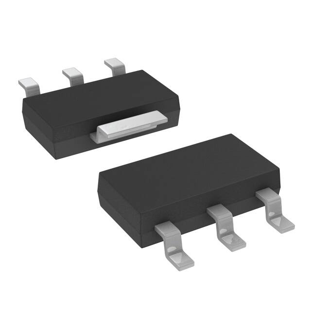
TO-252 (3)
6,6mm x 6,1mm
LM317MKTPR
PFM (3)
6,04mm x 6,15mm
KVU (TO-252) PACKAGE
(TOP VIEW)
INPUT
ADJUST
OUTPUT
OUTPUT
OUTPUT
OUTPUT
INPUT
BODY SIZE
SOT-223 (3)
KTP (PFM) PACKAGE
(TOP VIEW)
DCY (SOT-223) PACKAGE
(TOP VIEW)
PACKAGE
LM317MDCY
INPUT
OUTPUT
ADJUST
ADJUST
1
An IMPORTANT NOTICE at the end of this data sheet addresses availability, warranty, changes, use in safety-critical applications,
intellectual property matters and other important disclaimers. PRODUCTION DATA.
�LM317M
SLVS297P – APRIL 2000 – REVISED MARCH 2014
www.ti.com
Table of Contents
1
2
3
4
5
6
7
Features ..................................................................
Applications ...........................................................
Description .............................................................
Revision History.....................................................
Terminal Configuration and Functions................
Specifications.........................................................
1
1
1
2
3
3
6.1
6.2
6.3
6.4
6.5
6.6
3
3
3
4
4
5
Absolute Maximum Ratings .....................................
Handling Ratings.......................................................
Recommended Operating Conditions.......................
Thermal Information ..................................................
Electrical Characteristics...........................................
Typical Characteristics ..............................................
7.3 Feature Description................................................... 7
7.4 Device Functional Modes.......................................... 8
8
Applications and Implementation ........................ 9
8.1 Application Information.............................................. 9
8.2 Typical Application .................................................... 9
9 Power Supply Recommendations...................... 11
10 Layout................................................................... 11
10.1 Layout Guidelines ................................................. 11
10.2 Layout Example .................................................... 11
11 Device and Documentation Support ................. 12
Detailed Description .............................................. 7
11.1 Trademarks ........................................................... 12
11.2 Electrostatic Discharge Caution ............................ 12
11.3 Glossary ................................................................ 12
7.1 Overview ................................................................... 7
7.2 Functional Block Diagram ......................................... 7
12 Mechanical, Packaging, and Orderable
Information ........................................................... 12
4 Revision History
Changes from Revision O (July 2006) to Revision P
Page
•
Removed Ordering Information Table ................................................................................................................................... 1
•
Clarified TJ package field ....................................................................................................................................................... 3
2
Submit Documentation Feedback
Copyright © 2000–2014, Texas Instruments Incorporated
Product Folder Links: LM317M
�LM317M
www.ti.com
SLVS297P – APRIL 2000 – REVISED MARCH 2014
5 Terminal Configuration and Functions
ADJUST
INPUT
OUTPUT
OUTPUT
INPUT
OUTPUT
INPUT
OUTPUT
KVU (TO-252) PACKAGE
(TOP VIEW)
KTP (PFM) PACKAGE
(TOP VIEW)
DCY (SOT-223) PACKAGE
(TOP VIEW)
OUTPUT
ADJUST
ADJUST
Terminal Functions
TERMINAL
NAME
NO.
I/O
DESCRIPTION
ADJUST
1
I
Output feedback voltage
OUTPUT
2
O
Regulated output voltage
INPUT
3
–
Input supply voltage, 2.5 to 40V relative to OUTPUT terminal
6 Specifications
6.1 Absolute Maximum Ratings (1)
over operating temperature range (unless otherwise noted)
MIN
VI – VO
Input-to-output differential voltage
TJ
Operating virtual junction temperature
(1)
MAX
UNIT
40
V
150
°C
Stresses beyond those listed under "absolute maximum ratings" may cause permanent damage to the device. These are stress ratings
only, and functional operation of the device at these or any other conditions beyond those indicated under "recommended operating
conditions" is not implied. Exposure to absolute-maximum-rated conditions for extended periods may affect device reliability.
6.2 Handling Ratings
TSTG
Storage temperature range
MIN
MAX
UNIT
–65
150
°C
MIN
MAX
UNIT
2.5
37
V
0.01
0.5
A
0
125
–40
125
6.3 Recommended Operating Conditions
VI – VO
Input-to-output voltage differential
IO
Output current
LM317MKTPR
TJ
Operating virtual junction temperature
LM317MDCY,
LM317MDCYR,
LM317MKVURG3,
LM317MQKTPR,
LM317MQDCYR,
LM317MQDCYRG3
Submit Documentation Feedback
Copyright © 2000–2014, Texas Instruments Incorporated
Product Folder Links: LM317M
°C
3
�LM317M
SLVS297P – APRIL 2000 – REVISED MARCH 2014
www.ti.com
6.4 Thermal Information
LM317M
THERMAL METRIC (1)
DCY
UNIT
4 TERMINALS
RθJA
Junction-to-ambient thermal resistance
60.2
RθJCtop
Junction-to-case (top) thermal resistance
42.0
RθJB
Junction-to-board thermal resistance
9.4
ψJT
Junction-to-top characterization parameter
3.4
ψJB
Junction-to-board characterization parameter
9.3
RθJCbot
Junction-to-case (bottom) thermal resistance
n/a
(1)
°C/W
For more information about traditional and new thermal metrics, see the IC Package Thermal Metrics application report, SPRA953.
6.5 Electrical Characteristics
over recommended operating virtual-junction temperature range, VI – VO = 5 V, IO = 0.1 A (unless otherwise noted)
TEST CONDITIONS (1)
PARAMETER
Line regulation (2)
VI – VO = 3 V to 40 V
Load regulation
IO = 10 mA to 500 mA
TYP
MAX
TJ = 25°C
MIN
0.01
0.04
Full temperature range
0.02
0.07
TJ = 25°C
0.1
0.5
Full temperature range
0.3
1.5
50
100
μA
0.2
5
μA
1.25
1.3
V
ADJUST terminal current
Change in ADJUST terminal current
VI – VO = 3 V to 40 V,
IO = 10 mA to 500 mA
Reference voltage
VI – VO = 3 V to 40 V,
IO = 10 mA to 500 mA
1.2
Output-voltage temperature stability
0.7
Minimum load current
to maintain regulation
3.5
Maximum output current
VI – VO ≤ 15 V
VI – VO = 40 V, PD ≤ PD(max),
TJ = 25°C
f = 10 Hz to 10 kHz,
TJ = 25°C
Ripple rejection
VO = 10 V, f = 120 Hz,
TJ = 25°C
CADJ = 0 (3)
Long-term stability
TJ = 25°C
RMS output noise voltage (% of VO)
(1)
(2)
(3)
4
CADJ = 10 μF (3)
500
900
150
250
0.003
65
66
80
0.3
UNIT
%/V
%VO
%
10
mA
mA
%VO
dB
1 %/1k hrs
Pulse-testing techniques are used to maintain the junction temperature as close to the ambient temperature as possible.
Line voltage regulation is expressed here as the percentage change in output voltage per 1-V change at the input.
CADJ is connected between the ADJUST terminal and ground.
Submit Documentation Feedback
Copyright © 2000–2014, Texas Instruments Incorporated
Product Folder Links: LM317M
�LM317M
www.ti.com
SLVS297P – APRIL 2000 – REVISED MARCH 2014
6.6 Typical Characteristics
1.00
0.15
∆VO − Output Voltage Change − %
∆VO − Output Voltage Change − %
0.90
0.20
VI = 4.25 V to 41.25 V
VO = Vref
IL = 10 mA
0.80
0.70
0.60
0.50
0.40
0.30
0.20
0.10
0
VI = 45 V
VO = 5 V
IL = 10 mA to 100 mA
0.10
0.05
0.00
−0.05
−0.10
−0.15
VI = 10 V
VO = 5 V
IL = 10 mA to 40 mA
−0.20
−0.25
−0.30
−0.35
0
25
50
75
100
−0.40
125
0
25
TJ − Temperature − °C
Figure 1. Line Regulation vs Temperature
100
125
1.260
VI = 6.25 V
VO = Vref
1.255
VI = 4.25 V
VO = Vref
IL = 10 mA
51
IL = 100 mA
V ref − Reference Voltage − V
ADJUST Terminal Current − µA
75
Figure 2. Load Regulation vs Temperature
55
53
50
TJ − Temperature − °C
49
IL = 10 mA
47
45
43
41
39
1.245
1.240
1.235
1.230
1.225
37
35
1.250
0
25
75
50
100
1.220
125
0
TJ − Temperature − °C
25
50
75
100
125
TJ − Temperature − °C
Figure 3. Adjust Terminal Current vs Temperature
Figure 4. Temperature Stability vs Temperature
8
1.00
TJ = 125°C
6
TJ = 25°C
IO – Output Current – A
Minimum Operating Current − mA
7
5
TJ = 25°C
4
3
2
0.80
0.60
TJ = 125°C
0.40
0.20
1
0.00
0
0
5
10
15
20
25
30
35
0
40
5
10
15
20
25
30
35
40
VI – VO – Input-Output Differential – V
VI − VO − Input-Output Differential − V
Figure 5. Minimum Operating Current vs Input-output
Differential Voltage
Figure 6. Output Current Limit vs Input-output Differential
Voltage
Submit Documentation Feedback
Copyright © 2000–2014, Texas Instruments Incorporated
Product Folder Links: LM317M
5
�LM317M
SLVS297P – APRIL 2000 – REVISED MARCH 2014
www.ti.com
Typical Characteristics (continued)
0.004
90
VI = 15 Vdc and 1 VPP (120 Hz)
VO = 10 V
IL = 100 mA
CL = 1 µF
Ci = 0.1 µF
80
0.003
Ripple Rejection − dB
Ouput Noise Voltage − % VO
85
0.002
75
CADJ = 10 µF
70
65
60
0.001
CADJ = 0 µF
55
VI = 15 V
VO = 10 V
IL = 50 mA
Bandwidth = 10 Hz to 10 kHz
50
45
0.000
0
25
50
75
100
0
125
25
Figure 7. Output Noise Voltage vs Temperature
(VI − V O ) − Input-Output Voltage Differential − V
2.5
90
80
Ripple Rejection − dB
CADJ = 10 µF
70
60
50
CADJ = 0 µF
40
30
10
125
Figure 8. Ripple Rejection vs Temperature
100
20
85
70
TJ − Temperature − °C
TJ − Temperature − °C
VI = 15 Vdc and Vac = 1 VPP
VO = 10 V
IL = 100 mA
CL = 1 µF
Ci = 0.1 µF
0
10 Hz
100 Hz
2
IL = 500 mA
1.5
IL = 100 mA
1
0.5
0
1 kHz
10 kHz
0
100 kHz
25
50
75
100
125
TJ − Temperature − °C
Frequency
Figure 10. Input-output Voltage Differential vs Temperature
Figure 9. Ripple Rejection vs Frequency
10.00
VI = 15 V
VO = 10 V
IL = 100-mA dc and 10-mA RMS
Output Impedance − Ω
CADJ = 0 µF
1.00
CADJ = 10 µF
0.10
0.01
10 Hz
50 Hz
100 Hz
500 Hz
1 kHz
5 kHz
10 kHz
50 kHz
100 kHz
150 kHz
Frequency
Figure 11. Output Impedance vs Frequency
6
Submit Documentation Feedback
Copyright © 2000–2014, Texas Instruments Incorporated
Product Folder Links: LM317M
�LM317M
www.ti.com
SLVS297P – APRIL 2000 – REVISED MARCH 2014
7 Detailed Description
7.1 Overview
The LM317 is a 500-mA linear regulator with high voltage tolerance up to 40-V. The device has a feedback
voltage that is relative to the output instead of ground. This ungrounded design allows the LM317 to have
superior line and load regulation. It also allows the LM317 to be used as a current source or current sink using a
single resistor. Any output voltage output voltage from 1.25-V to 37-V can be obtained by using two resistors.
The bias current of the device, up to 10-mA, flows to the output; this current must be used by the load or the
feedback resistors. The power dissipation will be the product of pass element voltage and current,
mathematically:
(V[input] – V[output]) × I[output]
(1)
The application heat sink must be able to absorb this power.
7.2 Functional Block Diagram
Input
Iadj
+
1.25V
Adj.
Over Temp &
Over Current
Protection
Output
7.3 Feature Description
7.3.1 NPN Darlington Output Drive
NPN Darlington output topology provides naturally low output impedance and an output capacitor is optional. To
support maximum current and lowest temperature, 2.5-V headroom is recommended (VI – VO ).
7.3.2 Overload Block
Current limit scales with higher voltage to provide a safe operation area for the NPN pass elements. Over
temperature shutdown protects against overload or under heat sinking.
7.3.3 Programmable Feedback
Op amp with 1.25-V offset input at the ADJUST terminal provides easy output voltage or current (not both)
programming. For current regulation applications, a single resistor whose resistance value is 1.25V/IOUT and
power rating is greater than (1.25V)2/R should be used. For voltage regulation applications, two resistors set the
output voltage. See the Typical Application section for schematic and resistor formula.
Submit Documentation Feedback
Copyright © 2000–2014, Texas Instruments Incorporated
Product Folder Links: LM317M
7
�LM317M
SLVS297P – APRIL 2000 – REVISED MARCH 2014
www.ti.com
Feature Description (continued)
7.3.4 Current Sources
The two current sources represent the typical ‘adjust terminal current’ and typical ‘minimum current for
regulation'.
7.4 Device Functional Modes
7.4.1 Normal operation
The device OUTPUT terminal will source current necessary to make OUTPUT terminal 1.25-V greater than
ADJUST terminal to provide output regulation.
7.4.2 Operation With Low Input Voltage
The device requires up to 2.5-V headroom (Vin-Vout) to operate in regulation. With less headroom, the device
may drop out and OUTPUT voltage will be INPUT voltage minus drop out voltage.
7.4.3 Operation at Light Loads
The device passes its bias current to the OUTPUT terminal. The load or feedback must consume this minimum
current for regulation or the output may be too high.
7.4.4 Operation In Self Protection
When an overload occurs the device will shut down Darlington NPN output stage or reduce the output current to
prevent device damage. The device will automatically reset from the overload. The output may be reduced or
alternate between on and off until the overload is removed.
7.4.5 Operation at Light Loads
The device passes its bias current to the OUTPUT terminal. The load or feedback must consume this minimum
current for regulation or the output may be too high.
8
Submit Documentation Feedback
Copyright © 2000–2014, Texas Instruments Incorporated
Product Folder Links: LM317M
�LM317M
www.ti.com
SLVS297P – APRIL 2000 – REVISED MARCH 2014
8 Applications and Implementation
8.1 Application Information
The LM317M is a linear voltage regulator. The feedback is the output terminal to adjust terminal differential. The
output voltage can be set to any value from 1.25-V to Vout maximum with two resistors.
8.2 Typical Application
D1
1N4002
Input
VI
Output
LM317M
Adjust
IADJ
Vref=1.25V
VO
R1
240 Ω
D2
1N4002
CI
1.0 μF
CI
0.1 μF
R2
CADJ
8.2.1 Design Requirements
For this design example, use the parameters listed in Table 1.
Table 1. Design Parameters
DESIGN PARAMETER
EXAMPLE VALUE
Input voltage range
(Output Voltage + 2.5V) to 37V
Output voltage
Vref × (1 + R2/R1) + Iadj × R2
8.2.2 Detailed Design Procedure
8.2.2.1 Input Capacitor
An input capacitor is not required, but it is recommended, particularly if the regulator is not in close proximity to
the power-supply filter capacitors. A 0.1-µF ceramic or 1-µF tantalum provides sufficient bypassing for most
applications, especially when adjustment and output capacitors are used.
8.2.2.2 Output Capacitor
An output capacitor improves transient response, but it not needed for stability.
8.2.2.3 Feedback Resistors
The feedback resistor set the output voltage using Equation 2.
Vref × (1 + R2/R1) + Iadj × R2
(2)
8.2.2.4 Adjustment Terminal Capacitor
The optional adjustment terminal capacitor will improve ripple rejection by preventing the amplification of the
ripple. When capacitor is used and VOUT > 6V, a protection diode from adjust to output is recommended.
Submit Documentation Feedback
Copyright © 2000–2014, Texas Instruments Incorporated
Product Folder Links: LM317M
9
�LM317M
SLVS297P – APRIL 2000 – REVISED MARCH 2014
www.ti.com
8.2.2.5 Protection Diodes
If the input is shorted to ground during a fault condition, protection diode (D1) prevents discharge through the
LM317M. If the output is shorted to ground during a fault condition, protection diode (D2) prevents adjust terminal
capacitor discharge through the LM317M.
8.2.2.6 Design Options and Parameters
Common Linear Regulator designs are concerned with the following parameters:
•
•
•
•
•
•
•
•
Input voltage range
Input Capacitor range
Output voltage
Output current rating
Output capacitor range
Input Short Protection
Stability
Ripple Rejection
8.2.2.7 Output Voltage
Vo is calculated as shown:
Vo
V ref
R2
u (1 �
) � ( I adj u R 2 )
R1
(3)
Because Iadj typically is 50-µA, it is negligible in most applications.
8.2.2.8 Ripple Rejection
CADJ is used to improve ripple rejection; it prevents amplification of the ripple as the output voltage is adjusted
higher. If CADJ is used, it is best to include protection diodes.
8.2.2.9 Input Short Protection
If the input is shorted to ground during a fault condition, protection diodes provide measures to prevent the
possibility of external capacitors discharging through low-impedance paths in the IC. By providing low-impedance
discharge paths for CO and CADJ, respectively, D1 and D2 prevent the capacitors from discharging into the output
of the regulator.
0.6
0.4
0.2
0
VO = 10 V
VI = 15 V, ∆VI = +1 V
IL = 50 mA
TJ = 25°C
CL = 0 µF
CADJ = 0 µF
−0.2
−0.4
−0.6
−0.8
−1
∆V I − Input Voltage Change − V
∆V O − Output Voltage Change − V
1
0.8
1.2
1
0.8
0.6
0.4
0.2
0
−1.0
−0.5
0
0.5
1.0
1.5
2.0
2.5
3.0
3.5
4.0
Time − µs
Figure 12. Line Transient Response vs Time
10
5.0
4.0
3.0
2.0
VI = 15 V
VO = 10 V
IL = 50 mA
∆IL = +500 mA
CL = 1 µF
CADJ = 10 µF
1.0
0
−1.0
−2.0
CL = 0 µF
CADJ = 0 µF
−3.0
4.5
∆ I O − Output Current Change − A
∆V O − Output Voltage Change − V
8.2.3 Application Curves
−4.0
0.6
0.5
0.4
0.3
0.2
0.1
0
−0.1
−0.2
−10
−5
0
5
10
15
20
25
30
35
Time − µs
Figure 13. Load Transient Response vs Time
Submit Documentation Feedback
Copyright © 2000–2014, Texas Instruments Incorporated
Product Folder Links: LM317M
�LM317M
www.ti.com
SLVS297P – APRIL 2000 – REVISED MARCH 2014
9 Power Supply Recommendations
The LM317 is designed to operate from an input voltage supply range between 2.5-V to 40-V greater than the
output voltage. If the device is more than six inches from the input filter capacitors, an input bypass capacitor,
0.1-µF or greater, of any type is needed for stability.
10 Layout
10.1 Layout Guidelines
•
•
•
It is recommended that the input terminal be bypassed to ground with a bypass-capacitor.
The optimum placement is closest to the VIN and GND terminals of the device. Care must be taken to
minimize the loop area formed by the bypass-capacitor connection, the VIN terminal, and the GND terminal of
the IC.
For operation at full rated load, it is recommended to use wide trace lengths to eliminate IR drop and heat
dissipation.
10.2 Layout Example
OUTPUT
Ground
COUT
R2
Power
INPUT
OUTPUT
R1
ADJ/GND
Cadj
High
Frequency
Bypass
Capacitor
0.1μF
10μF
High Input
Bypass
Capacitor
Ground
Submit Documentation Feedback
Copyright © 2000–2014, Texas Instruments Incorporated
Product Folder Links: LM317M
11
�LM317M
SLVS297P – APRIL 2000 – REVISED MARCH 2014
www.ti.com
11 Device and Documentation Support
11.1 Trademarks
All trademarks are the property of their respective owners.
11.2 Electrostatic Discharge Caution
This integrated circuit can be damaged by ESD. Texas Instruments recommends that all integrated circuits be handled with
appropriate precautions. Failure to observe proper handling and installation procedures can cause damage.
ESD damage can range from subtle performance degradation to complete device failure. Precision integrated circuits may be more
susceptible to damage because very small parametric changes could cause the device not to meet its published specifications.
11.3 Glossary
SLYZ022 — TI Glossary.
This glossary lists and explains terms, acronyms and definitions.
12 Mechanical, Packaging, and Orderable Information
The following pages include mechanical packaging and orderable information. This information is the most
current data available for the designated devices. This data is subject to change without notice and revision of
this document. For browser-based versions of this data sheet, refer to the left-hand navigation.
12
Submit Documentation Feedback
Copyright © 2000–2014, Texas Instruments Incorporated
Product Folder Links: LM317M
�PACKAGE OPTION ADDENDUM
www.ti.com
13-Aug-2021
PACKAGING INFORMATION
Orderable Device
Status
(1)
Package Type Package Pins Package
Drawing
Qty
Eco Plan
(2)
Lead finish/
Ball material
MSL Peak Temp
Op Temp (°C)
Device Marking
(3)
(4/5)
(6)
LM317MDCY
ACTIVE
SOT-223
DCY
4
80
RoHS & Green
SN
Level-2-260C-1 YEAR
-40 to 125
L4
LM317MDCYG3
ACTIVE
SOT-223
DCY
4
80
RoHS & Green
SN
Level-2-260C-1 YEAR
-40 to 125
L4
LM317MDCYR
ACTIVE
SOT-223
DCY
4
2500
RoHS & Green
SN
Level-2-260C-1 YEAR
-40 to 125
L4
LM317MDCYRG3
ACTIVE
SOT-223
DCY
4
2500
RoHS & Green
SN
Level-2-260C-1 YEAR
-40 to 125
L4
LM317MKVURG3
ACTIVE
TO-252
KVU
3
2500
RoHS & Green
SN
Level-3-260C-168 HR
-40 to 125
LM317M
LM317MQDCYR
ACTIVE
SOT-223
DCY
4
2500
RoHS & Green
NIPDAU
Level-2-260C-1 YEAR
-40 to 125
L5
LM317MQDCYRG4
ACTIVE
SOT-223
DCY
4
2500
RoHS & Green
NIPDAU
Level-2-260C-1 YEAR
-40 to 125
L5
(1)
The marketing status values are defined as follows:
ACTIVE: Product device recommended for new designs.
LIFEBUY: TI has announced that the device will be discontinued, and a lifetime-buy period is in effect.
NRND: Not recommended for new designs. Device is in production to support existing customers, but TI does not recommend using this part in a new design.
PREVIEW: Device has been announced but is not in production. Samples may or may not be available.
OBSOLETE: TI has discontinued the production of the device.
(2)
RoHS: TI defines "RoHS" to mean semiconductor products that are compliant with the current EU RoHS requirements for all 10 RoHS substances, including the requirement that RoHS substance
do not exceed 0.1% by weight in homogeneous materials. Where designed to be soldered at high temperatures, "RoHS" products are suitable for use in specified lead-free processes. TI may
reference these types of products as "Pb-Free".
RoHS Exempt: TI defines "RoHS Exempt" to mean products that contain lead but are compliant with EU RoHS pursuant to a specific EU RoHS exemption.
Green: TI defines "Green" to mean the content of Chlorine (Cl) and Bromine (Br) based flame retardants meet JS709B low halogen requirements of