LM3202
650mA Miniature, Adjustable, Step-Down DC-DC
Converter for RF Power Amplifiers
General Description
Features
The LM3202 is a DC-DC converter optimized for powering
RF power amplifiers (PAs) from a single Lithium-Ion cell,
however they may be used in many other applications. It
steps down an input voltage from 2.7V to 5.5V to a variable
output voltage from 1.3V to 3.16V. Output voltage is set
using a VCON analog input for controlling power levels and
efficiency of the RF PA.
n
n
n
n
n
n
The LM3202 offers superior performance for mobile phones
and similar RF PA applications. Fixed-frequency PWM operation minimizes RF interference. Shutdown function turns
the device off and reduces battery consumption to 0.01 µA
(typ.).
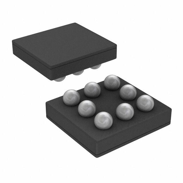
The LM3202 is available in a 8-pin lead free micro SMD
package. A high switching frequency (2 MHz) allows use of
tiny surface-mount components. Only three small external
surface-mount components, an inductor and two ceramic
capacitors are required.
n
n
n
n
2 MHz (typ.) PWM Switching Frequency
Operates from a single Li-Ion cell (2.7V to 5.5V)
Variable Output Voltage (1.3V to 3.16V)
Fast Output Voltage Transient (1.3V to 3.16V in 20µs)
650mA Maximum load capability
High Efficiency (96% Typ at 3.6VIN, 3.16VOUT at 400mA)
from internal synchronous rectification
8-pin micro SMD Package
Current Overload Protection
Thermal Overload Protection
Soft Start function
Applications
n
n
n
n
Cellular Phones
Hand-Held Radios
RF PC Cards
Battery Powered RF Devices
Typical Application
20141501
FIGURE 1. LM3202 Typical Application
© 2005 National Semiconductor Corporation
DS201415
www.national.com
LM3202 650mA Miniature, Adjustable, Step-Down DC-DC Converter for RF Power Amplifiers
October 2005
�LM3202
Connection Diagrams
20141599
8–Bump Thin Micro SMD Package, Large Bump
NS Package Number TLA08GNA
Order Information
Order Number
Package Marking (Note)
Supplied As
LM3202TL
XTS/29
250 units, Tape-and-Reel
LM3202TLX
XTS/29
3000 units, Tape-and-Reel
Note: The actual physical placement of the package marking will vary from part to part. The package marking “X” designates the date
code. “T” is a NSC internal code for die traceability. “S” designates the device type as switcher device. Both will vary considerably. “29”
identifies the device (part number, option, etc.).
Pin Descriptions
Pin #
Name
A1
PVIN
Description
Power Supply Voltage Input to the internal PFET switch.
B1
VDD
Analog Supply Input.
C1
EN
Enable Input. Set this digital input high for normal operation. For shutdown, set low.
C2
VCON
C3
FB
B3
SGND
Analog and Control Ground
A3
PGND
Power Ground
A2
SW
www.national.com
Voltage Control Analog input. VCON controls VOUT in PWM mode.
Feedback Analog Input. Connect to the output at the output filter capacitor.
Switch node connection to the internal PFET switch and NFET synchronous rectifier.
Connect to an inductor with a saturation current rating that exceeds the maximum Switch Peak
Current Limit specification of the LM3202.
2
�ESD Rating (Notes 4, 13)
Human Body Model:
Machine Model:
If Military/Aerospace specified devices are required,
please contact the National Semiconductor Sales Office/
Distributors for availability and specifications.
VDD, PVIN to SGND
−0.2V to +6.0V
PGND to SGND
−0.2V to +0.2V
EN, FB, VCON
(SGND −0.2V)
to (VDD +0.2V)
w/6.0V max
2 kV
200V
Operating Ratings (Notes 1, 2)
Input Voltage Range
2.7V to 5.5V
Recommended Load Current
Junction Temperature (TJ) Range
−30˚C to +125˚C
−30˚C to +85˚C
SW
(PGND −0.2V)
to (PVIN +0.2V)
w/6.0V max
Ambient Temperature (TA) Range
(Note 5)
PVIN to VDD
−0.2V to +0.2V
Thermal Properties
Continuous Power Dissipation
(Note 3)
Internally Limited
Junction Temperature (TJ-MAX)
+150˚C
0mA to 650mA
Junction-to-Ambient Thermal
Storage Temperature Range
−65˚C to +150˚C
Maximum Lead Temperature
(Soldering, 10 sec)
+260˚C
100˚C/W
Resistance (θJA), TLA08 Package
(Note 6)
Electrical Characteristics (Notes 2, 7, 8) Limits in standard typeface are for TA = TJ = 25˚C. Limits in boldface type apply over the full operating ambient temperature range (−30˚C ≤ TA = TJ ≤ +85˚C). Unless otherwise noted, all
specifications apply to LM3202 with: PVIN = VDD = EN = 3.6V.
Symbol
Parameter
Conditions
Min
Typ
Max
Units
1.21
1.30
1.39
V
VFB, MIN
Feedback Voltage at minimum
setting
VCON = 0.4V(Note 8)
VFB
Feedback Voltage
VCON = 1.1V(Note 8)
2.693
2.75
2.835
V
VFB, MAX
Feedback Voltage at maximum VCON = 1.4V(Note 8)
setting
3.03
3.17
3.29
V
ISHDN
Shutdown supply current
EN = SW = VCON = 0V,
(Note 9)
0.01
2
µA
IQ
DC bias current into VDD
VCON = 1V, FB = 0V,
No Switching (Note 10)
1
1.4
mA
RDSON(P)
Pin-pin resistance for PFET
ISW = 200mA
140
200
230
mΩ
RDSON(N)
Pin-pin resistance for NFET
ISW = -200mA
300
415
485
mΩ
(Note 11)
ILIM,PFET
Switch peak current limit
935
1100
1200
mA
FOSC
Internal oscillator frequency
1.7
2
2.3
MHz
VIH,EN
Logic high input threshold
1.2
VIL,EN
Logic low input threshold
0.5
V
5
10
µA
0.484
0.52
0.556
V
1.208
1.27
1.312
V
IPIN,ENABLE Pin pull down current
VCON,MIN
VCON Threshold
Commanding VFB,MIN
VCON,MAX VCONThreshold
Commanding VFB,MAX
ZCON
VCON input resistance
Gain
VCON to VOUT Gain
VCON swept down(Note 8)
VCON swept up(Note 8)
V
100
0.556V ≤ VCON ≤ 1.208V
3
kΩ
2.5
V/V
www.national.com
LM3202
Absolute Maximum Ratings (Notes 1, 2)
�LM3202
System Characteristics The following spec table entries are guaranteed by design providing the component
values in the typical application circuit are used. These parameters are not guaranteed by production testing. Min and
Max limits apply over the full operating ambient temperature range (−30˚C ≤ TA ≤ 85˚C) and over the VIN range = 2.7V to
5.5V unless otherwise specified, Typical values are at TA = 25˚C, PVIN = VDD = EN = 3.6V unless otherwise specified, L =
3.3µH, DCR of L ≤ 100mΩ, CIN = 10µF, 0603, 6.3V (4.7µF||4.7µF, 0603, 6.3V can also be used), COUT = 4.7µF, 0603, 6.3V
Symbol
Parameter
Typ
Max
VIN = 4.2V, COUT = 4.7µF, L = 3.3µH,
RLOAD = 5Ω
20
30
Time for VOUT to fall from
3.16V to 1.3V
VIN = 4.2V, COUT = 4.7µF, L = 3.3µH,
RLOAD = 10Ω
20
30
CCON
VCON input capacitance
VCON = 1V,
Test frequency = 100 kHz
Linearity
Linearity in control
range 0.556V to 1.208V
VIN = 3.6V
Monotonic in nature
ICON
Control pin input current
T_ON
Turn on time
(time for output to reach
3.16V from Enable low to
high transition)
TRESPONSE Time for VOUT to rise from
1.3V to 3.16V
η
Conditions
EN = Low to High, VIN = 4.2V, VO = 3.16V,
COUT = 4.7µF, IOUT ≤ 1mA
Min
Units
µs
20
pF
-3
+3
%
-10
10
µA
750
µs
210
VIN = 3.6V, VOUT = 1.3V, IOUT = 90mA
87
%
VIN = 3.6V, VOUT = 3.16V, IOUT = 400mA
96
%
VOUT_ripple Ripple voltage, PWM mode
VIN = 3V to 4.5V, VOUT = 1.3V, IOUT = 10mA
to 400mA (Note 12)
10
mVp-p
Line_tr
VIN = 600mV perturbance, over Vin range 3V
to 5.5V
TRISE = TFALL = 10µs, VOUT = 1.3V, IOUT =
100mA
50
mVpk
Efficiency
(L = 3.3µH, DCR ≤ 100mΩ)
Line transient response
Load_tr
Load transient response
VIN = 3.1/3.6/4.5V, VOUT = 1.3V, transients
up to 100mA, TRISE = TFALL = 10µs
50
mVpk
PSRR
VIN = 3.6V, VOUT = 1.3V,
IOUT = 100mA
sine wave perturbation
frequency = 10kHz, amplitude = 100mVp-p
40
dB
Note 1: Absolute Maximum Ratings indicate limits beyond which damage to the component may occur. Operating Ratings are conditions under which operation of
the device is guaranteed. Operating Ratings do not imply guaranteed performance limits. For guaranteed performance limits and associated test conditions, see the
Electrical Characteristics tables.
Note 2: All voltages are with respect to the potential at the GND pins. The LM3202 is designed for mobile phone applications where turn-on after power-up is
controlled by the system controller and where requirements for a small package size overrule increased die size for internal Under Voltage Lock-Out (UVLO) circuitry.
Thus, it should be kept in shutdown by holding the EN pin low until the input voltage exceeds 2.7V.
Note 3: Internal thermal shutdown circuitry protects the device from permanent damage. Thermal shutdown engages at TJ = 150˚C (typ.) and disengages at TJ =
130˚C (typ.).
Note 4: The Human body model is a 100pF capacitor discharged through a 1.5kΩ resistor into each pin. (MIL-STD-883 3015.7) The machine model is a 200pF
capacitor discharged directly into each pin.
Note 5: In applications where high power dissipation and/or poor package thermal resistance is present, the maximum ambient temperature may have to be
de-rated. Maximum ambient temperature (TA-MAX) is dependent on the maximum operating junction temperature (TJ-MAX-OP = 125˚C), the maximum power
dissipation of the device in the application (PD-MAX), and the junction-to ambient thermal resistance of the part/package in the application (θJA), as given by the
following equation: TA-MAX = TJ-MAX-OP – (θJA x PD-MAX).
Note 6: Junction-to-ambient thermal resistance (θJA) is taken from thermal measurements, performed under the conditions and guidelines set forth in the JEDEC
standard JESD51-7. A 4 layer, 4" x 4", 2/1/1/2 oz. Cu board as per JEDEC standards is used for the measurements.
Note 7: Min and Max limits are guaranteed by design, test, or statistical analysis. Typical numbers are not guaranteed, but do represent the most likely norm. Due
to the pulsed nature of the testing TA = TJ for the electrical characteristics table.
Note 8: The parameters in the electrical characteristics table are tested under open loop conditions at PVIN = VDD = 3.6V. For performance over the input voltage
range and closed loop results refer to the datasheet curves.
Note 9: Shutdown current includes leakage current of PFET.
Note 10: IQ specified here is when the part is operating at 100% duty cycle.
Note 11: Current limit is built-in, fixed, and not adjustable. Refer to datasheet curves for closed loop data and its variation with regards to supply voltage and
temperature. Electrical Characteristic table reflects open loop data (FB = 0V and current drawn from SW pin ramped up until cycle by cycle limit is activated). Closed
loop current limit is the peak inductor current measured in the application circuit by increasing output current until output voltage drops by 10%.
Note 12: Ripple voltage should measured at COUT electrode on good layout PC board and under condition using suggested inductors and capacitors.
Note 13: National Semiconductor recommends that all integrated circuits be handled with appropriate precautions. Failure to observe proper ESD handling
techniques can result in damage.
www.national.com
4
�Shutdown Current vs Temperature
(VCON = 0V, EN = 0V)
Quiescent Current vs Supply Voltage
(VCON = 2V, FB = 0V, No Switching)
20141557
20141556
Output Voltage vs Supply Voltage
(VOUT = 1.3V: low clamp)
Switching Frequency Variation vs Temperature
(VOUT = 1.3V, IOUT = 200mA)
20141558
20141555
Output Voltage vs Temperature
(VIN = 3.6V, VOUT = 3.16V: high clamp)
Output Voltage vs Temperature
(VIN = 3.6V, VOUT = 1.3V: low clamp)
20141559
20141510
5
www.national.com
LM3202
Typical Performance Characteristics (Circuit in Figure 3, PVIN = VDD = EN = 3.6V, L = 3.3uH, DCR
of L ≤ 100mΩ, CIN = 10uF, 0603, 6.3V ( 4.7uF||4.7uF, 0603, 6.3V can be used), COUT = 4.7uF, 0603, 6.3V unless otherwise
noted)
�LM3202
Typical Performance Characteristics (Circuit in Figure 3, PVIN = VDD = EN = 3.6V, L = 3.3uH, DCR
of L ≤ 100mΩ, CIN = 10uF, 0603, 6.3V ( 4.7uF||4.7uF, 0603, 6.3V can be used), COUT = 4.7uF, 0603, 6.3V unless otherwise
noted) (Continued)
Open/Closed Loop Current Limit vs Temperature
(PWM mode)
VCON Voltage vs Output Voltage
(VIN = 4.2V, RLOAD = 8Ω)
20141561
20141562
Efficiency vs Output Current
(VOUT = 1.3V)
Efficiency vs Output Voltage
(VIN = 3.6V)
20141563
20141564
Efficiency vs Output Current
(VOUT = 3.16V)
20141565
www.national.com
6
�Load Transient Response
(VOUT = 1.3V)
Load Transient Response
(VOUT = 3.16V)
20141516
20141517
Startup
(VIN= 4.2V, VOUT = 3.16V, IOUT < 1mA)
Startup
(VIN = 3.6V, VOUT = 1.3V, IOUT < 1mA)
20141518
20141581
Line Transient Response
(VIN = 3.0V to 3.6V, IOUT = 100mA)
Shutdown Response
(VIN = 4.2V, VOUT = 3.16V, RLOAD = 10Ω)
20141520
20141519
7
www.national.com
LM3202
Typical Performance Characteristics (Circuit in Figure 3, PVIN = VDD = EN = 3.6V, L = 3.3uH, DCR
of L ≤ 100mΩ, CIN = 10uF, 0603, 6.3V ( 4.7uF||4.7uF, 0603, 6.3V can be used), COUT = 4.7uF, 0603, 6.3V unless otherwise
noted) (Continued)
�LM3202
Typical Performance Characteristics (Circuit in Figure 3, PVIN = VDD = EN = 3.6V, L = 3.3uH, DCR
of L ≤ 100mΩ, CIN = 10uF, 0603, 6.3V ( 4.7uF||4.7uF, 0603, 6.3V can be used), COUT = 4.7uF, 0603, 6.3V unless otherwise
noted) (Continued)
VCON Voltage Response
(VIN = 4.2V, VCON = 0V/1.4V, RLOAD = 10Ω)
VCON and Load Transient
(VIN = 4.2V, VCON = 0V/1.4V, 15Ω/8Ω, same time)
20141522
20141521
Output Voltage Ripple
(VOUT = 1.3V)
Timed Current Limit Response
(VIN = 3.6V)
20141524
20141523
RDSON vs Temperature
(P-ch, ISW = 200mA)
Output Voltage Ripple in Pulse Skip
(VIN = 3.547V, VOUT = 3.16V, RLOAD = 5Ω)
20141525
20141576
www.national.com
8
�RDSON vs Temperature
(N-ch, ISW = -200mA)
EN High Threshold vs. Vin
20141577
20141579
VCON Threshold min vs. Vin
VCON Threshold max vs. Vin
20141584
20141585
VFB max vs. VIN
(VCON = 1.4V, RLOAD = 10Ω)
VFB min vs. VIN
(VCON = 0.4V,RLOAD = 10Ω
20141587
20141586
9
www.national.com
LM3202
Typical Performance Characteristics (Circuit in Figure 3, PVIN = VDD = EN = 3.6V, L = 3.3uH, DCR
of L ≤ 100mΩ, CIN = 10uF, 0603, 6.3V ( 4.7uF||4.7uF, 0603, 6.3V can be used), COUT = 4.7uF, 0603, 6.3V unless otherwise
noted) (Continued)
�LM3202
Block Diagram
20141535
FIGURE 2. Functional Block Diagram
Additional features include current overload protection, thermal overload shutdown and soft start.
The LM3202 is constructed using a chip-scale 8-pin micro
SMD package. This package offers the smallest possible
size, for space-critical applications such as cell phones,
where board area is an important design consideration. Use
of a high switching frequency (2MHz) reduces the size of
external components. As shown in Figure 1, only three external power components are required for implementation.
Use of a micro SMD package requires special design considerations for implementation. (See Micro SMD Package
Assembly and use in the Applications Information section.)
Its fine bump-pitch requires careful board design and precision assembly equipment. Use of this package is best suited
for opaque-case applications, where its edges are not subject to high-intensity ambient red or infrared light. Also, the
system controller should set EN low during power-up and
other low supply voltage conditions. (See Shutdown Mode in
the Device Information section.)
Operation Description
The LM3202 is a simple, step-down DC-DC converter optimized for powering RF power amplifiers (PAs) in mobile
phones, portable communicators, and similar battery powered RF devices. It is designed to allow the RF PA to operate
at maximum efficiency over a wide range of power levels
from a single Li-Ion battery cell. It is based on a currentmode buck architecture, with synchronous rectification for
high efficiency. It is designed for a maximum load capability
of 650mA in PWM mode.
Maximum load range may vary from this depending on input
voltage, output voltage and the inductor chosen.
Efficiency is typically around 96% for a 400mA load with
3.16V output, 3.6V input. The output voltage is dynamically
programmable from 1.3V (typ) to 3.16V (typ) by adjusting the
voltage on the control pin without the need for external
feedback resistors. This ensures longer battery life by being
able to change the PA supply voltage dynamically depending
on its transmitting power.
www.national.com
10
�LM3202
Operation Description
(Continued)
20141536
FIGURE 3. Typical Operating System Circuit
to ramp higher before the comparator turns off the PFET.
This increases the average current sent to the output and
adjusts for the increase in the load.
Before appearing at the PWM comparator, a slope compensation ramp from the oscillator is subtracted from the error
signal for stability of the current feedback loop. The minimum
on time of PFET in PWM mode is 50ns (typ.)
Circuit Operation
Referring to Figure 1 and Figure 2, the LM3202 operates as
follows. During the first part of each switching cycle, the
control block in the LM3202 turns on the internal PFET
(P-channel MOSFET) switch. This allows current to flow
from the input through the inductor to the output filter capacitor and load. The inductor limits the current to a ramp with a
slope of around (VIN - VOUT) / L, by storing energy in a
magnetic field. During the second part of each cycle, the
controller turns the PFET switch off, blocking current flow
from the input, and then turns the NFET (N-channel MOSFET) synchronous rectifier on. In response, the inductor’s
magnetic field collapses, generating a voltage that forces
current from ground through the synchronous rectifier to the
output filter capacitor and load. As the stored energy is
transferred back into the circuit and depleted, the inductor
current ramps down with a slope around VOUT / L. The
output filter capacitor stores charge when the inductor current is high, and releases it when low, smoothing the voltage
across the load.
Shutdown Mode
Setting the EN digital pin low ( < 0.5V) places the LM3202 in
a 0.01µA (typ.) Shutdown mode. During shutdown, the PFET
switch, NFET synchronous rectifier, reference voltage
source, control and bias circuitry of the LM3202 are turned
off. Setting EN high ( > 1.2V) enables normal operation.
EN should be set low to turn off the LM3202 during power-up
and under voltage conditions when the power supply is less
than the 2.7V minimum operating voltage. The LM3202 is
designed for compact portable applications, such as mobile
phones. In such applications, the system controller determines power supply sequencing and requirements for small
package size outweigh the additional size required for inclusion of UVLO (Under Voltage Lock-Out) circuitry.
The output voltage is regulated by modulating the PFET
switch on time to control the average current sent to the load.
The effect is identical to sending a duty-cycle modulated
rectangular wave formed by the switch and synchronous
rectifier at SW to a low-pass filter formed by the inductor and
output filter capacitor. The output voltage is equal to the
average voltage at the SW pin.
While in operation, the output voltage is regulated by switching at a constant frequency and then modulating the energy
per cycle to control power to the load. Energy per cycle is set
by modulating the PFET switch on-time pulse width to control the peak inductor current. This is done by comparing the
signal from the current-sense amplifier with a slope compensated error signal from the voltage-feedback error amplifier.
At the beginning of each cycle, the clock turns on the PFET
switch, causing the inductor current to ramp up. When the
current sense signal ramps past the error amplifier signal,
the PWM comparator turns off the PFET switch and turns on
the NFET synchronous rectifier, ending the first part of the
cycle. If an increase in load pulls the output down, the error
amplifier output increases, which allows the inductor current
Internal Synchronous Rectification
The LM3202 uses an internal NFET as a synchronous rectifier to reduce rectifier forward voltage drop and associated
power loss. Synchronous rectification provides a significant
improvement in efficiency whenever the output voltage is
relatively low compared to the voltage drop across and
ordinary rectifier diode.
The internal NFET synchronous rectifier is turned on during
the inductor current down slope in the second part of each
cycle. The synchronous rectifier is turned off prior to the next
cycle. The NFET is designed to conduct through its intrinsic
body diode during transient intervals before it turns on, eliminating the need for an external diode.
Current Limiting
A current limit feature allows the LM3202 to protect itself and
external components during overload conditions. In PWM
mode, an 1200mA (max.) cycle-by-cycle current limit is normally used. If an excessive load pulls the output voltage
11
www.national.com
�LM3202
Current Limiting
(Continued)
down to approximately 0.375V, then the device switches to a
timed current limit mode. In timed current limit mode the
internal PFET switch is turned off after the current comparator trips and the beginning of the next cycle is inhibited for
3.5us to force the instantaneous inductor current to ramp
down to a safe value. The synchronous rectifier is off in
timed current limit mode. Timed current limit prevents the
loss of current control seen in some products when the
output voltage is pulled low in serious overload conditions.
Dynamically Adjustable Output
Voltage
The LM3202 features dynamically adjustable output voltage
to eliminate the need for external feedback resistors. The
output can be set from VFB,MIN to VFB,MAX by changing the
voltage on the analog VCON pin. This feature is useful in PA
applications where peak power is needed only when the
handset is far away from the base station or when data is
being transmitted. In other instances the transmitting power
can be reduced. Hence the supply voltage to the PA can be
reduced, promoting longer battery life. See Setting the Output Voltage in the Application Information section for further
details.
20141562
FIGURE 4. VCON Voltage vs Output Voltage
Refer to Figure 4 for the relation between VOUT and VCON.
When the control pin voltage is between 0.556V and 1.208V,
the output voltage will vary in a monotonic fashion with
respect to the voltage on the control pin as per the above
Table 1 equation.
Internally the control pin is clamped before it is fed to the
error amplifier inputs. If voltage on the control pin is less than
0.484V, the output voltage is regulated at VFB,MIN and if the
voltage is greater than 1.312V, the output is regulated at
VFB,MAX.
Thermal Overload Protection
The LM3202 has a thermal overload protection function that
operates to protect itself from short-term misuse and overload conditions. When the junction temperature exceeds
around 150˚C, the device inhibits operation. Both the PFET
and the NFET are turned off in PWM mode. When the
temperature drops below 125˚C, normal operation resumes.
Prolonged operation in thermal overload conditions may
damage the device and is considered bad practice.
INDUCTOR SELECTION
A 3.3µH inductor with saturation current rating over 1200mA
is recommended for almost all applications. The inductor’s
resistance should be less than 0.2Ω for good efficiency. For
low dropout voltage, lower DCR inductors are advantageous. Using inductors that drop by 20% in value at 1200mA
over the operating temp range is acceptable if needed to
select smallest inductor. Table 2 suggests some inductors
and suppliers.
Application Information
SETTING THE OUTPUT VOLTAGE
The LM3202 features a pin-controlled variable output voltage to eliminate the need for external feedback resistors. It
can be programmed for an output voltage from 1.3V (typ) to
3.16V (typ) by setting the voltage on the VCON pin, as in
Table 1.
TABLE 2. Suggested inductors and their suppliers
Model
TABLE 1. Output Voltage Selection
VCON(V)
VOUT (V)
VCON ≤ 0.484
VFB,MIN
0.556 < VCON < 1.208
VOUT = 2.5 x VCON
VCON ≥ 1.312
VFB,MAX
Size (WxLxH) [mm]
Vendor
NR3015T3R3M
3.0 x 3.0 x 1.5
Taiyo-Yuden
DO3314-332MXC
3.3 x 3.3x 1.4
Coilcraft
If smaller inductance inductor is used in the application, the
LM3202 may become unstable during line and load transients and VCON transient response times may get affected.
For low-cost applications, an unshielded bobbin inductor is
suggested. For noise critical applications, a toroidal or
shielded-bobbin inductor should be used. A good practice is
to layout the board with footprints accommodating both
types for design flexibility. This allows substitution of a lownoise toroidal inductor, in the event that noise from low-cost
bobbin models is unacceptable. Saturation occurs when the
magnetic flux density from current through the windings of
the inductor exceeds what the inductor’s core material can
support with a corresponding magnetic field. This can cause
poor efficiency, regulation errors or stress to DC-DC converter like the LM3202.
www.national.com
12
�surface of the board and interfering with mounting. See
Application Note 1112 for specific instructions how to do this.
(Continued)
CAPACITOR SELECTION
The 8-Bump package used for LM3202 has 300micron solder balls and requires 10.82mil pads for mounting on the
circuit board. The trace to each pad should enter the pad
with a 90˚entry angle to prevent debris from being caught in
deep corners. Initially, the trace to each pad should be 7mil
wide, for a section approximately 7mil long , as a thermal
relief. Then each trace should neck up or down to its optimal
width. The important criterion is symmetry. This ensures the
solder bumps on the LM3202 re-flow evenly and that the
device solders level to the board. In particular, special attention must be paid to the pads for bumps A1, A3 and B3.
Because PGND and PVIN are typically connected to large
copper planes, inadequate thermal relief’s can result in late
or inadequate re-flow of these bumps.
The Micro SMD package is optimized for the smallest possible size in applications with red or infrared opaque cases.
Because the Micro SMD package lacks the plastic encapsulation characteristic of larger devices, it is vulnerable to light.
Backside metallization and/or epoxy coating, along with
front-side shading by the printed circuit board, reduce this
sensitivity. However, the package has exposed die edges. In
particular, Micro SMD devices are sensitive to light, in the
red and infrared range, shining on the package’s exposed
die edges.
The LM3202 is designed for ceramic capacitor for its input
and output filters. Use a 10µF ceramic capacitor for input
and a 4.7µF ceramic capacitor for output. Ceramic capacitors types such as X5R, X7R are recommended to use for
both filters. These provide an optimal balance between small
size, cost, reliability and performance for cell phones and
similar applications. Table 3 lists suggests some part numbers and suppliers. DC bias characteristics of the capacitors
must be considered when selecting the voltage rating and
case size of the capacitor. Smaller case sizes for the output
mitigates piezo electric vibrations of the capacitor when the
output voltage is stepped up and down at fast rates however
they have a bigger percentage drop in value with dc bias.
Use of multiple 2.2µF or 1µF capacitors can also be considered.
TABLE 3. Suggested capacitors and their suppliers
Model
Vendor
JMK212BJ475, 4.7µF, 6.3V
Taiyo-Yuden
GRM188R60J475, 4.7µF, 6.3V
MuRata
C2012X5R0J106,10µF, 6.3V
TDK
The input filter capacitor supplies AC current drawn by the
PFET switch of the LM3202 in the first part of each cycle and
reduces the voltage ripple imposed on the input power
source. The output filter capacitor absorbs the AC inductor
current, helps maintain a steady output voltage during transient load changes and reduces output voltage ripple. These
capacitors must be selected with sufficient capacitance and
sufficiently low ESR (Equivalent Series Resistance) to perform these functions. The ESR of the filter capacitors is
generally a major factor in voltage ripple.
BOARD LAYOUT CONSIDERATIONS
PC board layout is an important part of DC-DC converter
design. Poor board layout can disrupt the performance of a
DC-DC converter and surrounding circuitry by contributing to
EMI, ground bounce, and resistive voltage loss in the traces.
These can send erroneous signals to the DC-DC converter
IC, resulting in poor regulation or instability. Poor layout can
also result in re-flow problems leading to poor solder joints
between the Micro SMD package and board pads. Poor
solder joints can result in erratic or degraded performance.
Good layout for the LM3202 can be implemented by following a few simple design rules.
EN PIN CONTROL
Drive the EN pin using the system controller to turn the
LM3202 ON and OFF. Use a comparator, Schmidt trigger or
logic gate to drive the EN pin. Set EN high ( > 1.2V) for
normal operation and low ( < 0.5V) for a 0.01µA (typ.) shutdown mode.
1.
Place the LM3202 on 10.82mil pads. As a thermal relief,
connect to each pad with a 7mil wide, approximately
7mil long traces, and when incrementally increase each
trace to its optimal width. The important criterion is symmetry to ensure the solder bumps on the LM3202 re-flow
evenly (see Micro SMD Package Assembly and Use).
2. Place the LM3202, inductor and filter capacitors close
together and make the trace short. The traces between
these components carry relatively high switching currents and act as antennas. Following this rule reduces
radiated noise. Place the capacitors and inductor within
0.2inch (5mm) of the LM3202.
3. Arrange the components so that the switching current
loops curl in the same direction. During the first half of
each cycle, current flows from the input filter capacitor,
through the LM3202 and inductor to the output filter
capacitor and back through ground, forming a current
loop. In the second half of each cycle, current is pulled
up from ground, through the LM3202 by the inductor, to
the output filter capacitor and then back through ground,
forming a second current loop. Routing these loops so
the current curls in the same direction prevents magnetic field reversal between the two half-cycles and reduces radiated noise.
Set EN low to turn off the LM3202 during power-up and
under voltage conditions when the power supply is less than
the 2.7V minimum operating voltage. The part is out of
regulation when the input voltage is less than 2.7V. The
LM3202 is designed for mobile phones where the system
controller controls operation mode for maximizing battery life
and requirements for small package size outweigh the additional size required for inclusion of UVLO (Under Voltage
Lock-Out) circuitry.
Micro SMD PACKAGE ASSEMBLY AND USE
Use of the Micro SMD package requires specialized board
layout, precision mounting and careful re-flow techniques, as
detailed in National Semiconductor Application Note 1112.
Refer to the section Surface Mount Technology (SMD) Assembly Considerations. For best results in assembly, alignment ordinals on the PC board should be used to facilitate
placement of the device. The pad style used with Micro SMD
package must be the NSMD (non-solder mask defined) type.
This means that the solder-mask opening is larger than the
pad size. This prevents a lip that otherwise forms if the
solder-mask and pad overlap, from holding the device off the
13
www.national.com
LM3202
Application Information
�LM3202
Application Information
power connections to the DC-DC converter circuit. This
reduces voltage errors caused by resistive losses across
the traces
(Continued)
4.
Connect the ground pins of the LM3202, and filter capacitors together using generous component-side copper fill as a pseudo-ground plane. Then connect this to
the ground-plane (if one is used) with several vias. This
reduces ground-plane noise by preventing the switching
currents from circulating through the ground plane. It
also reduces ground bounce at the LM3202 by giving it
a low-impedance ground connection.
5. Use wide traces between the power components and for
www.national.com
6.
14
Route noise sensitive traces, such as the voltage feedback path, away from noisy traces between the power
components. The voltage feedback trace must remain
close to the LM3202 circuit and should be routed directly
from FB to VOUT at the output capacitor and should be
routed opposite to noise components. This reduces EMI
radiated onto the DC-DC converter’s own voltage feedback trace.
�inches (millimeters) unless otherwise noted
8-Bump Thin Micro SMD, Large Bump
X1 = 1.666mm ± 0.030mm
X2 = 1.819mm ± 0.030mm
X3 = 0.600mm ± 0.075mm
NS Package Number TLA08GNA
National does not assume any responsibility for use of any circuitry described, no circuit patent licenses are implied and National reserves
the right at any time without notice to change said circuitry and specifications.
For the most current product information visit us at www.national.com.
LIFE SUPPORT POLICY
NATIONAL’S PRODUCTS ARE NOT AUTHORIZED FOR USE AS CRITICAL COMPONENTS IN LIFE SUPPORT DEVICES OR SYSTEMS
WITHOUT THE EXPRESS WRITTEN APPROVAL OF THE PRESIDENT AND GENERAL COUNSEL OF NATIONAL SEMICONDUCTOR
CORPORATION. As used herein:
1. Life support devices or systems are devices or systems
which, (a) are intended for surgical implant into the body, or
(b) support or sustain life, and whose failure to perform when
properly used in accordance with instructions for use
provided in the labeling, can be reasonably expected to result
in a significant injury to the user.
2. A critical component is any component of a life support
device or system whose failure to perform can be reasonably
expected to cause the failure of the life support device or
system, or to affect its safety or effectiveness.
BANNED SUBSTANCE COMPLIANCE
National Semiconductor manufactures products and uses packing materials that meet the provisions of the Customer Products
Stewardship Specification (CSP-9-111C2) and the Banned Substances and Materials of Interest Specification (CSP-9-111S2) and contain
no ‘‘Banned Substances’’ as defined in CSP-9-111S2.
Leadfree products are RoHS compliant.
National Semiconductor
Americas Customer
Support Center
Email: new.feedback@nsc.com
Tel: 1-800-272-9959
www.national.com
National Semiconductor
Europe Customer Support Center
Fax: +49 (0) 180-530 85 86
Email: europe.support@nsc.com
Deutsch Tel: +49 (0) 69 9508 6208
English Tel: +44 (0) 870 24 0 2171
Français Tel: +33 (0) 1 41 91 8790
National Semiconductor
Asia Pacific Customer
Support Center
Email: ap.support@nsc.com
National Semiconductor
Japan Customer Support Center
Fax: 81-3-5639-7507
Email: jpn.feedback@nsc.com
Tel: 81-3-5639-7560
LM3202 650mA Miniature, Adjustable, Step-Down DC-DC Converter for RF Power Amplifiers
Physical Dimensions
�