User's Guide
SNVA136A – June 2006 – Revised April 2013
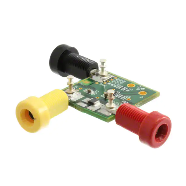
AN-1420 LM3208 Evaluation Board
1
Introduction
The LM3208 evaluation board is a working demonstration of a step down DC-DC converter. This
document contains information about the evaluation board and board layout considerations. For further
information on buck converter topology, device electrical characteristics, and component selection, see the
device-specific data sheet.
2
General Description
The LM3208 is a DC-DC converter optimized for powering RF power amplifiers (PAs) from a single
Lithium-Ion cell, however they may be used in many other applications. It steps down an input voltage
from 2.7V to 5.5V to a variable output voltage from 0.8V(typ.) to 3.6V(typ.). Output voltage is set using a
VCON analog input for controlling power levels and efficiency of the RF PA.
The LM3208 offers superior performance for mobile phones and similar RF PA applications. Fixedfrequency PWM operation minimizes RF interference. Shutdown function turns the device off and reduces
battery consumption to 0.01 µA (typ.).
The LM3208 is available in a 8-pin lead free DSBGA package. A high switching frequency (2 MHz) allows
use of tiny surface-mount components. Only three small external surface-mount components, an inductor
and two ceramic capacitors are required.
3
Operating Conditions
The board will operate under the following conditions:
• VIN range: 2.7V ≤ VIN ≤ 5.5V
• VCON range: 0.32V ≤ VCON ≤ 1.44V
• VOUT equation: VOUT = 2.5 x VCON
• IOUT range: 0 mA≤ IOUT ≤ 650 mA
4
Typical Application
VIN
C3 *
R1 0:
2.7V to 5.5V
PVIN
LM3208
C4 *
VCON
L1 3.0 PH
0.8V to 3.6V
SW
EN
C1
10 PF
VOUT
VDD
PGND
VOUT = 2.5 x VCON
FB
SGND
C2
4.7 PF
* : C3, C4 optional
All trademarks are the property of their respective owners.
SNVA136A – June 2006 – Revised April 2013
Submit Documentation Feedback
AN-1420 LM3208 Evaluation Board
Copyright © 2006–2013, Texas Instruments Incorporated
1
�Evaluation Board Layout
5
www.ti.com
Evaluation Board Layout
3.0 H
4.7 F
0
10 F
Figure 1. Top Layer
2
AN-1420 LM3208 Evaluation Board
SNVA136A – June 2006 – Revised April 2013
Submit Documentation Feedback
Copyright © 2006–2013, Texas Instruments Incorporated
�Connection Diagram and Package Mark Information
www.ti.com
677-002 rev A
Figure 2. Bottom Layer
6
Connection Diagram and Package Mark Information
Figure 3. 8-Bump Thin DSBGA Package, Large Bump
SNVA136A – June 2006 – Revised April 2013
Submit Documentation Feedback
AN-1420 LM3208 Evaluation Board
Copyright © 2006–2013, Texas Instruments Incorporated
3
�Bill of Materials (BOM) for Common Configurations
www.ti.com
Table 1. Pin Descriptions
7
Pin No
Name
A1
PVIN
Power Supply Voltage Input to the internal PFET switch.
Description
B1
VDD
Analog Supply Input.
C1
EN
Enable Input. Set this digital input high for normal operation. For shutdown, set low.
C2
VCON
C3
FB
B3
SGND
Analog and Control Ground
A3
PGND
Power Ground
A2
SW
Voltage Control Analog input. VCON controls VOUT in PWM mode.
Feedback Analog Input. Connect to the output at the output filter capacitor.
Switch node connection to the internal PFET switch and NFET synchronous rectifier.
Connect to an inductor with a saturation current rating that exceeds the maximum Switch Peak Current Limit
specification of the LM3208.
Bill of Materials (BOM) for Common Configurations
Manufacture
Manufacture No
Description
C1 (input C)
TDK
C2012X5R0J106M
10 µF, 6.3V, 20%, 0805 (2012)
C2 (output C)
TDK
C1608X5R0J475M
4.7 µF, 6.3V, 20%, 0603 (1608)
(1)
C3 (optional, input C)
0.1 µF, 25V , 0402 (1005)
C4 (optional, filter for VCON)
10 - 100 pF, 25V, 0402 (1005)
(1)
L1 (inductor)
FDK
MIPW3226D3R0M
3.0 µH, Idc = 1000mA, Rdc = 0.12Ω, 3.2×2.6×1.0 mm
R1 (jumper PVIN to VDD)
Vishay
CRCW04020R00F
0Ω, 0402 (1005)
VIN banana jack - red
Johnson
Components
108-0902-001
Connector, insulated banana jack (red)
Vout banana jack - yellow
Johnson
Components
108-0907-001
Connector, insulated banana jack (yellow)
GND banana jack - black
Johnson
Components
108-0903-001
Connector, insulated banana jack (black)
(1)
8
C3 and C4 are recommended for a better noise performance.
Board Layout Considerations
Fosc = 2 MHz
i
VIN
i
PVIN
+ C1 E
- 10 PF
L1
3.3 PH VOUT
VDD
SW
EN
FB
C2
4.7 PF
VCON
PGND
SGND
+
-
C
Figure 4. Current Loop
4
AN-1420 LM3208 Evaluation Board
SNVA136A – June 2006 – Revised April 2013
Submit Documentation Feedback
Copyright © 2006–2013, Texas Instruments Incorporated
�Board Layout Considerations
www.ti.com
The LM3208 converts higher input voltage to lower output voltage with high efficiency. This is achieved
with an inductor-based switching topology. During the first half of the switching cycle, the internal PMOS
switch turns on, the input voltage is applied to the inductor, and the current flows from PVIN line to the
output capacitor (C2) and the load through the inductor. During the second half cycle, the PMOS turns off
and the internal NMOS turns on. The inductor current continues to flow via the inductor from the device
PGND line to the output capacitor (C2) and the load .
Referring to Figure 4, a pulse current flows in the left hand side loop, and a ripple current flows in the right
hand side loop. Board layout and circuit pattern design of these two loops are the key factors for reducing
noise radiation and stable operation. In other lines, such as from battery to C1 and C2 to the load, the
current is mostly DC current. Theresore, it is not necessary to take so much care. Only pattern width
(current capability) and DCR drop considerations are needed.
8.1
Board Layout Flow
1. Minimize C1, PVIN, and PGND loop. These traces should be as wide and short as possible. This is the
highest priority.
2. Minimize L1, C2, SW and PGND loop. These traces also should be wide and short. This is the second
priority.
3. The above layout patterns should be placed on the component side of the PCB to minimize parasitic
inductance and resistance due to via-holes. It may be a good idea that the SW to L1 path is routed
between C1(+) and C1(-) land patterns. If vias are used in these large current paths, multiple via-holes
should be used if possible.
4. Connect C1(-), C2(-) and PGND with wide GND pattern. This pattern should be short, so C1(-), C2(-),
and PGND should be as close as possible. Then connect to a PCB common GND pattern with as
many via-holes as possible.
5. SGND should not connect directly to PGND. Connecting these pins under the device should be
avoided. (If possible, connect SGND to the common port of C1(-), C2(-) and PGND.)
6. VDD should not be connected directly to PVIN. Connecting these pins under the device should be
avoided. It is good idea to connect VDD to C1(+) to avoid switching noise injection to the VDD line.
7. The FB line should be protected from noise. It is a good idea to use an inner GND layer (if available)
as a shield.
NOTE: The evaluation board shown in Figure 1 and Figure 2 for the LM3208 was designed with
these considerations, and it shows good performance. However some aspects have not
been optimized because of limitations due to evaluation-specific requirements. The board
can be used as a reference, but it is not the ideal. For more information, contact a TI
representative.
SNVA136A – June 2006 – Revised April 2013
Submit Documentation Feedback
AN-1420 LM3208 Evaluation Board
Copyright © 2006–2013, Texas Instruments Incorporated
5
�IMPORTANT NOTICE
Texas Instruments Incorporated and its subsidiaries (TI) reserve the right to make corrections, enhancements, improvements and other
changes to its semiconductor products and services per JESD46, latest issue, and to discontinue any product or service per JESD48, latest
issue. Buyers should obtain the latest relevant information before placing orders and should verify that such information is current and
complete. All semiconductor products (also referred to herein as “components”) are sold subject to TI’s terms and conditions of sale
supplied at the time of order acknowledgment.
TI warrants performance of its components to the specifications applicable at the time of sale, in accordance with the warranty in TI’s terms
and conditions of sale of semiconductor products. Testing and other quality control techniques are used to the extent TI deems necessary
to support this warranty. Except where mandated by applicable law, testing of all parameters of each component is not necessarily
performed.
TI assumes no liability for applications assistance or the design of Buyers’ products. Buyers are responsible for their products and
applications using TI components. To minimize the risks associated with Buyers’ products and applications, Buyers should provide
adequate design and operating safeguards.
TI does not warrant or represent that any license, either express or implied, is granted under any patent right, copyright, mask work right, or
other intellectual property right relating to any combination, machine, or process in which TI components or services are used. Information
published by TI regarding third-party products or services does not constitute a license to use such products or services or a warranty or
endorsement thereof. Use of such information may require a license from a third party under the patents or other intellectual property of the
third party, or a license from TI under the patents or other intellectual property of TI.
Reproduction of significant portions of TI information in TI data books or data sheets is permissible only if reproduction is without alteration
and is accompanied by all associated warranties, conditions, limitations, and notices. TI is not responsible or liable for such altered
documentation. Information of third parties may be subject to additional restrictions.
Resale of TI components or services with statements different from or beyond the parameters stated by TI for that component or service
voids all express and any implied warranties for the associated TI component or service and is an unfair and deceptive business practice.
TI is not responsible or liable for any such statements.
Buyer acknowledges and agrees that it is solely responsible for compliance with all legal, regulatory and safety-related requirements
concerning its products, and any use of TI components in its applications, notwithstanding any applications-related information or support
that may be provided by TI. Buyer represents and agrees that it has all the necessary expertise to create and implement safeguards which
anticipate dangerous consequences of failures, monitor failures and their consequences, lessen the likelihood of failures that might cause
harm and take appropriate remedial actions. Buyer will fully indemnify TI and its representatives against any damages arising out of the use
of any TI components in safety-critical applications.
In some cases, TI components may be promoted specifically to facilitate safety-related applications. With such components, TI’s goal is to
help enable customers to design and create their own end-product solutions that meet applicable functional safety standards and
requirements. Nonetheless, such components are subject to these terms.
No TI components are authorized for use in FDA Class III (or similar life-critical medical equipment) unless authorized officers of the parties
have executed a special agreement specifically governing such use.
Only those TI components which TI has specifically designated as military grade or “enhanced plastic” are designed and intended for use in
military/aerospace applications or environments. Buyer acknowledges and agrees that any military or aerospace use of TI components
which have not been so designated is solely at the Buyer's risk, and that Buyer is solely responsible for compliance with all legal and
regulatory requirements in connection with such use.
TI has specifically designated certain components as meeting ISO/TS16949 requirements, mainly for automotive use. In any case of use of
non-designated products, TI will not be responsible for any failure to meet ISO/TS16949.
Products
Applications
Audio
www.ti.com/audio
Automotive and Transportation
www.ti.com/automotive
Amplifiers
amplifier.ti.com
Communications and Telecom
www.ti.com/communications
Data Converters
dataconverter.ti.com
Computers and Peripherals
www.ti.com/computers
DLP® Products
www.dlp.com
Consumer Electronics
www.ti.com/consumer-apps
DSP
dsp.ti.com
Energy and Lighting
www.ti.com/energy
Clocks and Timers
www.ti.com/clocks
Industrial
www.ti.com/industrial
Interface
interface.ti.com
Medical
www.ti.com/medical
Logic
logic.ti.com
Security
www.ti.com/security
Power Mgmt
power.ti.com
Space, Avionics and Defense
www.ti.com/space-avionics-defense
Microcontrollers
microcontroller.ti.com
Video and Imaging
www.ti.com/video
RFID
www.ti-rfid.com
OMAP Applications Processors
www.ti.com/omap
TI E2E Community
e2e.ti.com
Wireless Connectivity
www.ti.com/wirelessconnectivity
Mailing Address: Texas Instruments, Post Office Box 655303, Dallas, Texas 75265
Copyright © 2013, Texas Instruments Incorporated
�