LM3350
LM3350 Switched Capacitor Voltage Converter
Literature Number: SNIS101B
�LM3350
Switched Capacitor Voltage Converter
General Description
Features
The LM3350 is a CMOS charge-pump voltage converter
which efficiently provides a 3.3V to 5V step-up, or 5V to 3.3V
step-down. The LM3350 uses four small, low cost capacitors
to provide the voltage conversion. It eliminates the cost, size
and radiated EMI related to inductor based circuits, or the
power loss of a linear regulator. Operating power conversion
efficiency greater than 90% provides ideal performance for
battery powered portable systems.
The architecture provides a fixed voltage conversion ratio of
3/2 or 2/3. Thus it can be used for other DC-DC conversions
as well.
■
■
■
■
■
Conversion of 3.3V to 5V, or 5V to 3.3V
4.2Ω typical step-up output impedance
1.8Ω typical step-down output impedance
90% typical power conversion efficiency at 50 mA
800 kHz switch frequency allows use of very small,
inexpensive capacitors.
■ No inductor required
■ 250 nA typical shutdown current
■ Small Mini SO-8 package
Applications
■
■
■
■
Any mixed 5V and 3.3V system
Laptop computers and PDAs
Handheld instrumentation
PCMCIA cards
Basic Operating Circuits
Step-Up Converter
10000201
Step-Down Converter
10000202
© 2010 National Semiconductor Corporation
100002
100002 Version 6 Revision 2
www.national.com
Print Date/Time: 2010/12/28 23:06:13
LM3350 Switched Capacitor Voltage Converter
OBSOLETE
December 28, 2010
�LM3350
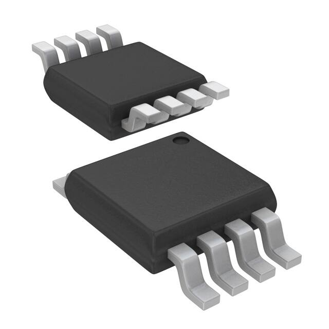
Connection Diagram
Mini SO8 Package
10000203
Top View
Ordering Information
Order Number
Package Type
NSC Package
Drawing
Package Marking
LM3350MMX
Mini SO-8
MUA08A
S00A
3500k Units on Tape and Reel
LM3350MM
Mini SO-8
MUA08A
S00A
1000 Units on Tape and Reel
Supplied As
Pin Descriptions
Pin
Name
Function
1
Cap1+ Positive terminal for the first charge pump
capacitor.
2
Cap1− Negative terminal for the first charge pump
capacitor.
3
Cap2+ Positive terminal for the second charge
pump capacitor.
4
Cap2− Negative terminal for the second charge
pump capacitor.
5
Vlow
In Step-Up mode, this will be the input
terminal. In Step-Down mode, this will be
the output terminal.
6
Gnd
Ground
7
Vhigh
In Step-Down mode, this will be the input
terminal. In Step-Up mode, this will be the
output terminal.
8
Enable Active high CMOS logic level Enable Input.
Connect to Voltage Input terminal to
enable the IC. Connect to Ground (Pin 6)
to disable.
www.national.com
2
100002 Version 6 Revision 2
Print Date/Time: 2010/12/28 23:06:13
�Operating Conditions
If Military/Aerospace specified devices are required,
please contact the National Semiconductor Sales Office/
Distributors for availability and specifications.
Maximum Input Voltage, Step-Down
Maximum Input Voltage, Step-Up
Power Dissipation (PD) (TA=25°C,
(Note 2))
5.5V
3.65V
500 mW
θja (Note 2)
Tj Max (Note 2)
Storage Temperature
Lead Temperature (Soldering, 10 secs)
ESD Susceptibility (Note 3)
Not short circuit protected.
250°C/W
(Note 1)
Ambient Temperature Range
−40°C to + 85°C
150°C
−65°C to +150°C
260°C
2kV
Electrical Characteristics
3/2 Step-Up Voltage Converter
Specifications in standard type face are for Tj = 25°C, and those with boldface type apply over full operating temperature
range. Unless otherwise specified, Vin = 3.3V, VEnable = 3.3V, Iload = 50 mA.
Conditions
Typ (Note 4)
VoutNL
Output Voltage at No
Load
C1, C2, Cin and Cout: 0.33µF, esr ≤ 0.33 Ω
at 1MHz. Iload = 0 A
5.0
V
VoutFL
Output Voltage at 50
mA
C1, C2, Cin and Cout: 0.33µF, esr ≤ 0.33 Ω
at 1MHz. Iload = 50 mA
4.7
V
Vin
Input Supply Voltage
Range
Symbol
IQ1
IQ2
Zout
fSW
VEnable
IEnable
Pη
Parameter
Quiescent Current
3.3
Shutdown Mode, VEnable = 0V, Iload=0 A;
Current into pin Vlow
0.025
Normal Mode, IIoad = 0A; Current into pin
VIow
3.75
Output Source
Impedance
Iload = 50 mA
4.2
Switching Frequency
(Note 6)
Quiescent Current
V
V(Min)
V(Max)
3
µA
µA(Max)
5
mA
mA(Max)
6.25
Ω (Max)
500
1100
kHz
kHz(Min)
kHz(Max)
1.0
2.5
V
V(Min)
V(Max)
1
µA
µA(Max)
Ω
1.7
Current into ENABLE pin; ENABLE = 5V
and all other pins at ground
Power Efficiency
0.025
90
3
100002 Version 6 Revision 2
Print Date/Time: 2010/12/28 23:06:13
Units
2.5
3.65
800
Enable Threshold
Voltage
Leakage Current
Limits (Note 5)
%
www.national.com
LM3350
Absolute Maximum Ratings (Note 1)
�LM3350
Electrical Characteristics
2/3 Step-Down Voltage Converter
Specifications in standard type face are for Tj = 25°C, and those with boldface type apply over full operating temperature
range. Unless otherwise specified, Vhigh = 5V, VEnable = 5V, Iload = 50 mA.
Conditions
Typ (Note 4)
VoutNL
Output Voltage at No
Load
C1, C2, Cin and Cout: 0.33µF, esr ≤ 0.33 Ω
at 1MHz. Iload = 0 A
3.3
V
VoutFL
Output Voltage at 50
mA
C1, C2, Cin and Cout: 0.33 µF, esr ≤ 0.33Ω
at 1MHz. Iload =50 mA
3.2
V
Vin
Input Supply Voltage
Range
Symbol
IQ1
IQ2
Zout
fSW
VEnable
IEnable
Pη
Parameter
Quiescent Current
5
Shutdown Mode, VEnable = 0V, Iload=0 A;
Current into pin Vhigh
0.25
Normal Mode, IIoad = 0A; Current into pin
Vhigh
2.5
Output Source
Impedance
Iload = 50 mA
1.8
Switching Frequency
(Note 6)
Quiescent Current
V
V(Min)
V(Max)
3
µA
µA(Max)
3.3
mA
mA(Max)
3
Ω (Max)
500
1100
kHz
kHz(Min)
kHz(Max)
1.0
2.5
V
V(Min)
V(Max)
1
µA
µA(Max)
Ω
1.7
Current into ENABLE pin; ENABLE = 5V
and all other pins at ground
Power Efficiency
Units
2.2
5.5
800
Enable Threshold
Voltage
Leakage Current
Limits (Note 5)
0.025
90
%
Note 1: Absolute maximum ratings indicate limits beyond which damage to the device may occur. Operating ratings indicate conditions for which the device is
intended to be functional, but do not guarantee specific performance limits. For guaranteed specifications and test conditions, see Electrical Characteristics. The
guaranteed specifications apply only for the test conditions listed. Some performance characteristics may degrade when the device is not operated under the
listed test conditions.
Note 2: For operation at elevated temperatures, LM3350 must be derated based on package thermal resistance of θja and Tj max, Tj = TA+ θjaPD.
Note 3: The human body model is a 100 pF capacitor discharged through a 1.5 kW resistor into each pin.
Note 4: Typical numbers are at 25°C and represent the most likely parametric norm.
Note 5: Limits are 100% production tested at 25°C. Limits over the operating temperature range are guaranteed through correlation using Statistical Quality
Control (SQC) methods. The limits are used to calculate National's Averaging Outgoing Quality Level (AOQL).
Note 6: The internal oscillator runs at 1.6 MHz, the output switches operate at one half of the oscillator frequency, fOSC = 2fSW.
www.national.com
4
100002 Version 6 Revision 2
Print Date/Time: 2010/12/28 23:06:13
�LM3350
Typical Performance Characteristics
Vout vs Iload (Step-Up)
Pη vs Iload (Step-Up)
10000204
10000206
Output Source Impedance vs Temperature (Step-Up)
Vout vs Iload (Step-Down)
10000209
10000205
Output Source Impedance vs Temperature (Step-Down)
Pη vs Iload (Step-Down)
10000208
10000207
5
100002 Version 6 Revision 2
Print Date/Time: 2010/12/28 23:06:13
www.national.com
�LM3350
Switching Frequency vs Temperature
10000210
www.national.com
6
100002 Version 6 Revision 2
Print Date/Time: 2010/12/28 23:06:13
�OPERATING PRINCIPLE
The LM3350 is a charge-pump voltage converter that provides a voltage conversion ratio of 3/2 in step-up mode and a
conversion ratio of 2/3 in the step-down mode. Thus it can be
used in the step-down mode to provide a 3.3V output from a
regulated 5V input or in the step-up mode to provide a 5V
output from a regulated 3.3V input. Other values of input voltages can be used as long as they are within the limits.
The LM3350 contains an array of CMOS switches which are
operated in a certain sequence to provide the step-up or stepdown of the input supply. An internal RC oscillator provides
the timing signals.
Energy transfer and storage are provided by four inexpensive
ceramic capacitors. The selection of these capacitors is explained in the Capacitor Selection section under Application
Information.
where Iload is the load current and fO is the oscillator frequency.
In order to ensure superior performance over the entire operating temperature range, capacitors made of X7R dielectric
material are suggested. However, capacitors made of other
dielectric materials that still meet the ±20% specification over
the entire temperature range can also be used.
STEP-UP APPLICATIONS NEED AN EXTRA DIODE
The LM3350 is biased from pin Vhigh. Thus for step-up applications, an external Schottky diode (D1) is needed to supply
power to Vhigh during startup (See Figure 2). Note that during
shutdown, this diode will provide a DC path from Vin to Vout.
The load may therefore continue to draw current from the input voltage source. This Schottky diode is not required for
step-down applications (See Figure 3).
SHUTDOWN MODE
When ENABLE is a logic low (ground), the LM3350 enters a
low power shutdown mode. In this mode, all circuitry is disabled and therefore, all switching action stops. During shutdown, the current consumption drops to 250 nA (typical).
When ENABLE is a logic high, (i.e. 3.3V for step-up mode and
5.0V for step-down mode), the LM3350 returns to normal operation.
10000211
A. Step-Up Mode
Application Information
CAPACITOR SELECTION
The LM3350 requires four capacitors: an input bypass capacitor (connected between Vin and ground), an output hold
capacitor (connected between Vout and ground), and two
sampling capacitors (C1 and C2 in Figures 2, 3). 0.33 µF
(±20%) ceramic chip type capacitors are recommended for all
four capacitors. The usable operating frequency should be
greater than 5 MHz for all capacitors.
The input bypass capacitor (Cin) is the least critical. Its value
should be at least that of the sampling capacitors.
While the recommended sampling capacitor values are 0.33
µF, other values may be selected. Values other than 0.33 µF
affect maximum output current rating and efficiency. Figure
1 shows typical output impedance (Zout) versus capacitor value.
The output hold capacitor value determines the output ripple.
Increasing the value of the hold capacitor decreases the rip-
10000212
B. Step-Down Mode
FIGURE 1. Zout vs. C
PRECAUTIONS
The LM3350 is not short circuit protected.
7
100002 Version 6 Revision 2
Print Date/Time: 2010/12/28 23:06:13
www.national.com
LM3350
ple. The value of this capacitor (Cout) can be calculated (approximately) based on the output ripple (ΔVout) requirements
from:
Detailed Operation
�LM3350
Typical Application Circuits
10000213
FIGURE 2. Step-Up Converter
10000214
FIGURE 3. Step-Down Converter
and high frequency ringing. Of the four capacitors, Chigh and
Clow have the highest value of di/dt. It is therefore most important to keep them close to the IC. The ground lead that
Chigh and Clow share should also be kept wide and short.
The location of the diode (D1) used in the step-up configuration is not critical. This diode is only used during the initial turn
on of the IC. D1 is not needed in step-down applications.
Layout Information
LAYOUT CONSIDERATIONS
The LM3350's high switching frequency (800 kHz) makes a
good layout important. Figure 4 illustrates a typical layout. It
is important to keep the distance short between the four capacitors and the IC. Wide traces and grounding are also
recommended. These steps will minimize trace inductance
www.national.com
8
100002 Version 6 Revision 2
Print Date/Time: 2010/12/28 23:06:13
�LM3350
10000216
B. Actual Size of the Layout
10000215
A. Copper side (5X)
10000217
C. Copper side with Component Locations (5X)
FIGURE 4. Typical Layout
9
100002 Version 6 Revision 2
Print Date/Time: 2010/12/28 23:06:13
www.national.com
�LM3350
Physical Dimensions inches (millimeters) unless otherwise noted
8-Lead Mini SO (MM)
Order Number LM3350MMX or LM3350MM
NS Package Number MUA08A
www.national.com
10
100002 Version 6 Revision 2
Print Date/Time: 2010/12/28 23:06:13
�LM3350
Notes
11
100002 Version 6 Revision 2
Print Date/Time: 2010/12/28 23:06:13
www.national.com
�LM3350 Switched Capacitor Voltage Converter
Notes
For more National Semiconductor product information and proven design tools, visit the following Web sites at:
www.national.com
Products
Design Support
Amplifiers
www.national.com/amplifiers
WEBENCH® Tools
www.national.com/webench
Audio
www.national.com/audio
App Notes
www.national.com/appnotes
Clock and Timing
www.national.com/timing
Reference Designs
www.national.com/refdesigns
Data Converters
www.national.com/adc
Samples
www.national.com/samples
Interface
www.national.com/interface
Eval Boards
www.national.com/evalboards
LVDS
www.national.com/lvds
Packaging
www.national.com/packaging
Power Management
www.national.com/power
Green Compliance
www.national.com/quality/green
Switching Regulators
www.national.com/switchers
Distributors
www.national.com/contacts
LDOs
www.national.com/ldo
Quality and Reliability
www.national.com/quality
LED Lighting
www.national.com/led
Feedback/Support
www.national.com/feedback
Voltage References
www.national.com/vref
Design Made Easy
www.national.com/easy
www.national.com/powerwise
Applications & Markets
www.national.com/solutions
Mil/Aero
www.national.com/milaero
PowerWise® Solutions
Serial Digital Interface (SDI) www.national.com/sdi
Temperature Sensors
www.national.com/tempsensors SolarMagic™
www.national.com/solarmagic
PLL/VCO
www.national.com/wireless
www.national.com/training
PowerWise® Design
University
THE CONTENTS OF THIS DOCUMENT ARE PROVIDED IN CONNECTION WITH NATIONAL SEMICONDUCTOR CORPORATION
(“NATIONAL”) PRODUCTS. NATIONAL MAKES NO REPRESENTATIONS OR WARRANTIES WITH RESPECT TO THE ACCURACY
OR COMPLETENESS OF THE CONTENTS OF THIS PUBLICATION AND RESERVES THE RIGHT TO MAKE CHANGES TO
SPECIFICATIONS AND PRODUCT DESCRIPTIONS AT ANY TIME WITHOUT NOTICE. NO LICENSE, WHETHER EXPRESS,
IMPLIED, ARISING BY ESTOPPEL OR OTHERWISE, TO ANY INTELLECTUAL PROPERTY RIGHTS IS GRANTED BY THIS
DOCUMENT.
TESTING AND OTHER QUALITY CONTROLS ARE USED TO THE EXTENT NATIONAL DEEMS NECESSARY TO SUPPORT
NATIONAL’S PRODUCT WARRANTY. EXCEPT WHERE MANDATED BY GOVERNMENT REQUIREMENTS, TESTING OF ALL
PARAMETERS OF EACH PRODUCT IS NOT NECESSARILY PERFORMED. NATIONAL ASSUMES NO LIABILITY FOR
APPLICATIONS ASSISTANCE OR BUYER PRODUCT DESIGN. BUYERS ARE RESPONSIBLE FOR THEIR PRODUCTS AND
APPLICATIONS USING NATIONAL COMPONENTS. PRIOR TO USING OR DISTRIBUTING ANY PRODUCTS THAT INCLUDE
NATIONAL COMPONENTS, BUYERS SHOULD PROVIDE ADEQUATE DESIGN, TESTING AND OPERATING SAFEGUARDS.
EXCEPT AS PROVIDED IN NATIONAL’S TERMS AND CONDITIONS OF SALE FOR SUCH PRODUCTS, NATIONAL ASSUMES NO
LIABILITY WHATSOEVER, AND NATIONAL DISCLAIMS ANY EXPRESS OR IMPLIED WARRANTY RELATING TO THE SALE
AND/OR USE OF NATIONAL PRODUCTS INCLUDING LIABILITY OR WARRANTIES RELATING TO FITNESS FOR A PARTICULAR
PURPOSE, MERCHANTABILITY, OR INFRINGEMENT OF ANY PATENT, COPYRIGHT OR OTHER INTELLECTUAL PROPERTY
RIGHT.
LIFE SUPPORT POLICY
NATIONAL’S PRODUCTS ARE NOT AUTHORIZED FOR USE AS CRITICAL COMPONENTS IN LIFE SUPPORT DEVICES OR
SYSTEMS WITHOUT THE EXPRESS PRIOR WRITTEN APPROVAL OF THE CHIEF EXECUTIVE OFFICER AND GENERAL
COUNSEL OF NATIONAL SEMICONDUCTOR CORPORATION. As used herein:
Life support devices or systems are devices which (a) are intended for surgical implant into the body, or (b) support or sustain life and
whose failure to perform when properly used in accordance with instructions for use provided in the labeling can be reasonably expected
to result in a significant injury to the user. A critical component is any component in a life support device or system whose failure to perform
can be reasonably expected to cause the failure of the life support device or system or to affect its safety or effectiveness.
National Semiconductor and the National Semiconductor logo are registered trademarks of National Semiconductor Corporation. All other
brand or product names may be trademarks or registered trademarks of their respective holders.
Copyright© 2010 National Semiconductor Corporation
For the most current product information visit us at www.national.com
National Semiconductor
Americas Technical
Support Center
Email: support@nsc.com
www.national.com Tel: 1-800-272-9959
National Semiconductor Europe
Technical Support Center
Email: europe.support@nsc.com
100002 Version 6 Revision 2
National Semiconductor Asia
Pacific Technical Support Center
Email: ap.support@nsc.com
Print Date/Time: 2010/12/28 23:06:13
National Semiconductor Japan
Technical Support Center
Email: jpn.feedback@nsc.com
�IMPORTANT NOTICE
Texas Instruments Incorporated and its subsidiaries (TI) reserve the right to make corrections, modifications, enhancements, improvements,
and other changes to its products and services at any time and to discontinue any product or service without notice. Customers should
obtain the latest relevant information before placing orders and should verify that such information is current and complete. All products are
sold subject to TI’s terms and conditions of sale supplied at the time of order acknowledgment.
TI warrants performance of its hardware products to the specifications applicable at the time of sale in accordance with TI’s standard
warranty. Testing and other quality control techniques are used to the extent TI deems necessary to support this warranty. Except where
mandated by government requirements, testing of all parameters of each product is not necessarily performed.
TI assumes no liability for applications assistance or customer product design. Customers are responsible for their products and
applications using TI components. To minimize the risks associated with customer products and applications, customers should provide
adequate design and operating safeguards.
TI does not warrant or represent that any license, either express or implied, is granted under any TI patent right, copyright, mask work right,
or other TI intellectual property right relating to any combination, machine, or process in which TI products or services are used. Information
published by TI regarding third-party products or services does not constitute a license from TI to use such products or services or a
warranty or endorsement thereof. Use of such information may require a license from a third party under the patents or other intellectual
property of the third party, or a license from TI under the patents or other intellectual property of TI.
Reproduction of TI information in TI data books or data sheets is permissible only if reproduction is without alteration and is accompanied
by all associated warranties, conditions, limitations, and notices. Reproduction of this information with alteration is an unfair and deceptive
business practice. TI is not responsible or liable for such altered documentation. Information of third parties may be subject to additional
restrictions.
Resale of TI products or services with statements different from or beyond the parameters stated by TI for that product or service voids all
express and any implied warranties for the associated TI product or service and is an unfair and deceptive business practice. TI is not
responsible or liable for any such statements.
TI products are not authorized for use in safety-critical applications (such as life support) where a failure of the TI product would reasonably
be expected to cause severe personal injury or death, unless officers of the parties have executed an agreement specifically governing
such use. Buyers represent that they have all necessary expertise in the safety and regulatory ramifications of their applications, and
acknowledge and agree that they are solely responsible for all legal, regulatory and safety-related requirements concerning their products
and any use of TI products in such safety-critical applications, notwithstanding any applications-related information or support that may be
provided by TI. Further, Buyers must fully indemnify TI and its representatives against any damages arising out of the use of TI products in
such safety-critical applications.
TI products are neither designed nor intended for use in military/aerospace applications or environments unless the TI products are
specifically designated by TI as military-grade or "enhanced plastic." Only products designated by TI as military-grade meet military
specifications. Buyers acknowledge and agree that any such use of TI products which TI has not designated as military-grade is solely at
the Buyer's risk, and that they are solely responsible for compliance with all legal and regulatory requirements in connection with such use.
TI products are neither designed nor intended for use in automotive applications or environments unless the specific TI products are
designated by TI as compliant with ISO/TS 16949 requirements. Buyers acknowledge and agree that, if they use any non-designated
products in automotive applications, TI will not be responsible for any failure to meet such requirements.
Following are URLs where you can obtain information on other Texas Instruments products and application solutions:
Products
Applications
Audio
www.ti.com/audio
Communications and Telecom www.ti.com/communications
Amplifiers
amplifier.ti.com
Computers and Peripherals
www.ti.com/computers
Data Converters
dataconverter.ti.com
Consumer Electronics
www.ti.com/consumer-apps
DLP® Products
www.dlp.com
Energy and Lighting
www.ti.com/energy
DSP
dsp.ti.com
Industrial
www.ti.com/industrial
Clocks and Timers
www.ti.com/clocks
Medical
www.ti.com/medical
Interface
interface.ti.com
Security
www.ti.com/security
Logic
logic.ti.com
Space, Avionics and Defense
www.ti.com/space-avionics-defense
Power Mgmt
power.ti.com
Transportation and Automotive www.ti.com/automotive
Microcontrollers
microcontroller.ti.com
Video and Imaging
RFID
www.ti-rfid.com
OMAP Mobile Processors
www.ti.com/omap
Wireless Connectivity
www.ti.com/wirelessconnectivity
TI E2E Community Home Page
www.ti.com/video
e2e.ti.com
Mailing Address: Texas Instruments, Post Office Box 655303, Dallas, Texas 75265
Copyright © 2011, Texas Instruments Incorporated
�