National Semiconductor is now part of
Texas Instruments.
Search http://www.ti.com/ for the latest technical
information and details on our current products and services.
�LM3370
Dual Synchronous Step-Down DC-DC Converter with
Dynamic Voltage Scaling Function
General Description
Features
The LM3370 is a dual step-down DC-DC converter optimized
for powering ultra-low voltage circuits from a single Li-Ion battery and input rail ranging from 2.7V to 5.5V. It provides two
outputs with 600 mA load per channel. The output voltage
range varies from 1V to 3.3V and can be dynamically controlled using the I2C-compatible interface. This dynamic voltage scaling function allows processors to achieve maximum
performance at the lowest power level. The I2C-compatible
interface can also be used to control auto PFM-PWM/PWM
mode selection and other performance enhancing features.
The LM3370 offers superior features and performance for
portable systems with complex power management requirements. Automatic intelligent switching between PWM lownoise and PFM low-current mode offers improved system
efficiency. Internal synchronous rectification enhances the
converter efficiency without the use of further external devices.
There is a power-on-reset function that monitors the level of
the output voltage to avoid unexpected power losses. The independent enable pin for each output allows for simple and
effective power sequencing.
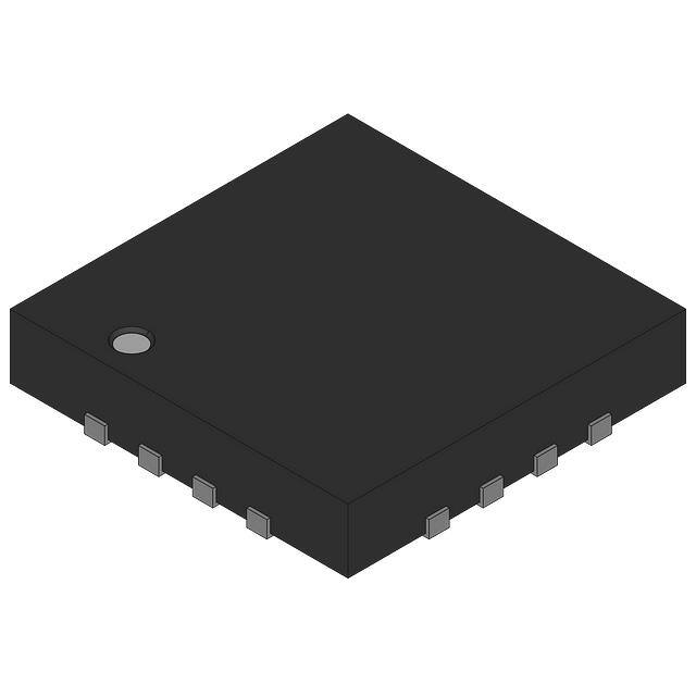
LM3370 is available in a 4 mm by 5 mm 16-lead non-pullback
LLP and a 20-bump micro SMD, 3.0 mm x 2.0 mm x 0.6 mm,
package. A high switching frequency—2 MHz (typ)—allows
use of tiny surface-mount components including a 2.2 µH inductor.
Default fixed voltages for the 2 output voltages combination
can be customized to fit system requirements by contacting
National Semiconductor Corporation.
■ I2C-compatible interface
■
■
■
■
■
■
■
■
■
■
■
— VOUT1 = 1V to 2V in 50 mV steps
— VOUT2 = 1.8V to 3.3V in 100 mV steps
— Automatic PFM/PWM mode switching & Forced PWM
mode for low noise operation
— Spread Spectrum capability using I2C
600 mA load per channel
2 MHz PWM fixed switching frequency (typ.)
The Bucks operate 180° out-of-phase timing offset for
noise and input surge current abatement
Internal synchronous rectification for high efficiency
Internal soft start
Power-on-reset function for both outputs
2.7V ≤ VIN ≤ 5.5V
Operates from a single Li-Ion cell or 3 cell NiMH/NiCd
batteries and 3.3V/5.5V fixed rails
2.2 µH Inductor, 4.7 µF Input and 10 µF Output Capacitor
per channel
16-lead LLP Package (4 mm x 5 mm x 0.8 mm)
20-bump micro SMD Package (3.0 mm x 2.0 mm x 0.6
mm)
Applications
■
■
■
■
Baseband Processors
Application Processors (Video, Audio)
I/O Power
FPGA Power and CPLD
Typical Performance Curve
20167381
© 2011 National Semiconductor Corporation
201673
www.national.com
LM3370 Dual Synchronous Step-Down DC-DC Converter with Dynamic Voltage Scaling Function
August 25, 2011
�LM3370
Typical Application Circuit
20167301
Functional Block Diagram
20167302
FIGURE 1. Functional Diagram
www.national.com
2
�LM3370
LLP Connection Diagram and Package Marking Information
20167343
•
•
•
The physical placement of the package marking will vary from part to part.
Date Code - UZXYTT format. ’U’ - Wafer fab code; ’Z’ - assembly site code; ’XY’ 2 digit date code; ’TT’ die run code
See National Web site for more info - http://www.national.com/quality/marking_conventions.html
Pin Descriptions (LLP)
Pin #
Name
1
VIN2
Power supply voltage input to PFET and NFET switches for Buck 2
Description
2
SW2
Buck 2 Switch Pin
3
PGND2
4
VDD
Buck 2 Power Ground
Signal supply voltage input, VDD must be equal or greater of the two inputs (VIN1 & VIN2)
5
SGND
Signal GND
6
PGND1
Buck 1 Power Ground
7
SW1
Buck 1 Switch Pin
8
VIN1
Power supply voltage input to PFET and NFET switches for Buck 1
9
FB1
Analog Feedback Input for Buck 1
10
SDA
I2C-Compatible Data, a 2 kΩ pull up resistor is required
11
SCL
I2C-Compatible Clock, a 2 kΩ pull up resistor is required
12
nPOR1
Power ON Reset for Buck 1, Open drain output Low when Buck 1 output is 92% of target
output. A 100 kΩ pull up resistor is required
13
nPOR2
Power ON Reset for Buck 2, Open drain output Low when Buck 2 output is 92% of target
output. A 100 kΩ pull up resistor is required
14
EN1
Buck 1 Enable
15
EN2
Buck 2 Enable
16
FB2
Analog feedback for Buck 2
3
www.national.com
�LM3370
Micro SMD Connection Diagram and Package Marking Information
20167379
Pin Descriptions (micro SMD)
Pin #
Name
A1
SW1
Buck 1 Switch Pin
Description
A2
VIN1
Power supply voltage input to PFET and NFET switches for Buck 1
A3
SGND
Signal GND
A4
FB1
B1
PGND1
B2
PGND1_S
B3
SDA
I2C-Compatible Data, a 2 kΩ pullup resistor is required
B4
SCL
I2C-Compatible Clock, a 2 kΩ pullup resistor is required
C1
VDD
Signal supply voltage input, VDD must be equal or greater of the two inputs ( VIN1 & VIN2)
C2
SGND
Signal GND
C3
nPOR1
Power ON Reset for Buck 1, Open drain output Low when Buck 1 output is 92% of target
output. A 100 kΩ pullup resistor is required
C4
nPOR2
Power ON Reset for Buck 2, Open drain output Low when Buck 2 output is 92% of target
output. A 100 kΩ pullup resistor is required
D1
PGND2
Buck 2 Power Ground
D2
PGND2_S
D3
EN2
Buck 2 Enable
D4
EN1
Buck 1 Enable
E1
SW2
Buck 2 Switch Pin
E2
VIN2
Power supply voltage input to PFET and NFET switches for Buck 2
E3
SGND
E4
FB2
www.national.com
Analog Feedback Input for Buck 1
Buck 1 Power Ground
Buck 1 Power Ground Sense
Buck 2 Power Ground Sense
Signal GND
Analog feedback for Buck 2
4
�LM3370
I2C Controlled Features
Features
Parameter
Comments
Output Voltage
VOUT1 & VOUT2
Output voltage is controlled via I2C-compatible
Modes
Buck 1 & Buck 2
Mode can be controlled via I2C
compatible by either forcing device
in Auto mode or forced PWM mode
Spread Spectrum
Buck 1 & Buck 2
Spread Spectrum capability via I2C-compatible for noise reduction
Ordering Information
(LLP)
Order Number
LM3370SD-3013
LM3370SDX-3013
LM3370SD-3021
LM3370SDX-3021
LM3370SD-3416
LM3370SDX-3416
LM3370SD-3621
LM3370SDX-3621
LM3370SD-3806
LM3370SDX-3806
LM3370SD-4221
LM3370SDX-4221
Voltage Option
1.2V & 2.5V
1.2V & 3.3V
1.4V & 2.8V
1.5V & 3.3V
1.6V & 1.8V
1.8V & 3.3V
Package Marking
Supplied As
S0003UB
1000 units, Tape-and-Reel
S0003UB
4500 units, Tape and Reel
S0003TB
1000 units, Tape-and-Reel
S0003TB
4500 units, Tape-and-Reel
S0003VB
1000 units, Tape-and-Reel
S0003VB
4500 units, Tape-and-Reel
S0004AB
1000 units, Tape-and-Reel
S0004AB
4500 units, Tape-and-Reel
S0003XB
1000 units, Tape-and-Reel
S0003XB
4500 units, Tape-and-Reel
S0003YB
1000 units, Tape-and-Reel
S0003YB
4500 units, Tape-and-Reel
(micro SMD)
Order Number
LM3370TL-2613 NOPB
LM3370TLX-2613 NOPB
LM3370TL-3607 NOPB
LM3370TLX-3607 NOPB
LM3370TL-3008 NOPB
LM3370TLX-3008 NOPB
LM3370TL-3006 NOPB
LM3370TLX-3006 NOPB
LM3370TL-3806 NOPB
LM3370TLX-3806 NOPB
LM3370TL-3206 NOPB
LM3370TLX-3206 NOPB
LM3370TL-3022 NOPB
LM3370TLX-3022 NOPB
Voltage Option
Package Marking
1.0V & 2.5V
1.5V & 1.9V
1.2V & 2.0V
1.2V & 1.8V
1.6V & 1.8V
1.3V & 1.8V
1.2V & 1.85V
Supplied As
SD1B
250 units, Tape-and-Reel
SD1B
3000 units, Tape-and-Reel
SPSB
250 units, Tape-and-Reel
SPSB
3000 units, Tape-and-Reel
SPTB
250 units, Tape-and-Reel
SPTB
3000 units, Tape-and-Reel
SPUB
250 units, Tape-and-Reel
SPUB
3000 units, Tape-and-Reel
SPVB
250 units, Tape-and-Reel
SPVB
3000 units, Tape-and-Reel
SPXB
250 units, Tape-and-Reel
SPXB
3000 units, Tape-and-Reel
STHB
250 units, Tape-and-Reel
STHB
3000 units, Tape-and-Reel
Note the LM3370TL-3607 has the following default output voltages where VOUT1 = 1.5V & VOUT2 = 1.9V
5
www.national.com
�LM3370
ESD Ratings (Note 5)
All Pins
Absolute Maximum Ratings (Note 1, Note
2 kV HBM
200V MM
2)
If Military/Aerospace specified devices are required,
please contact the National Semiconductor Sales Office/
Distributors for availability and specifications.
Operating Ratings
(Note 1, Note 2)
Input Voltage Range ((Note 10))
2.7V to 5.5V
Recommended Load Current Per
0 mA to 600 mA
Channel
Junction Temperature (TJ) Range
−30°C to +125°C
Ambient Temperature (TA) Range (Note −30°C to +85°C
6)
VIN1 , VIN2 VDD to PGND &
SGND
−0.2V to 6V
PGND to SGND
−0.2V to +0.2V
SDA, SCL, EN, EN2, nPOR1,
nPOR2, SW1, SW2, FB1 & FB2 (GND - 0.2) to (VIN + 0.2V)
Maximum Continuous Power
Dissipation (PD_MAX) (Note 3)
Internally Limited
Junction Temperature (TJ-MAX)
125°C
Storage Temperature Range
−65°C to +150°C
Maximum Lead Temperature
(Soldering)
(Note 4)
Thermal Properties
(Note 7)
Junction-to-Ambient Thermal Resistance
θJA (LLP-16)
26°C/W
θJA (20-Bump micro SMD)
50°C/W
Electrical Characteristics
(Note 2, Note 8, Note 10) Typical limits appearing in normal type apply for TJ = 25°
C. Limits appearing in boldface type apply over the entire junction temperature range (TA = TJ = −30°C to +85°C). Unless otherwise
noted, VIN1 = VIN2 = 3.6V.
Symbol
Parameter
Conditions
VFB
Feedback Voltage
(Note 11)
VOUT
Line Regulation
Min
Typ
−3.5
Max
+3.5
Units
%
2.7V ≤ VIN ≤ 5.5V
IO = 10 mA, VOUT = 1.8V
0.031
%/V
Load Regulation
100 mA ≤ IO ≤ 600 mA
VIN = 3.6V, VOUT = 1.8V
0.0013
%/mA
IQ PFM
Quiescent Current “On”
PFM Mode, Both Bucks ON
34
µA
IQ SD
Quiescent Current “Off”
EN1 = EN2 = 0V
ILIM
Peak Switching Current Limit
VIN = 3.6V
RDS_ON
(LLP)
PFET
NFET
RDS_ON
PFET
(micro SMD) NFET
FOSC
Internal Oscillator Frequency
IEN
Enable (EN) Input Current
VIL
Enable Logic Low
VIH
Enable Logic High
0.2
3
µA
1200
1400
mA
VIN = 3.6V, ISW = 200 mA
390
500
VIN = 3.6V, ISW = 200 mA
240
350
VIN = 3.6V, ISW = 200 mA
350
400
VIN = 3.6V, ISW = 200 mA
170
210
2.0
2.4
MHz
0.01
1
µA
0.4
V
850
1.5
mΩ
mΩ
V
1.0
POWER ON RESET THRESHOLD/FUNCTION (POR)
nPOR1 &
nPOR2
Delay Time
nPOR1 = Power ON Reset
for Buck 1
nPOR2 = Power ON Reset
for Buck 2
50 mS (default)
POR
Threshold
Percentage of Target VOUT
VOUT Rising
94
VOUT Falling, 85% (default), Can be
pre-trimmed to 70% or 94%
85
www.national.com
Can be pre-trimmd to 50 uS, 100
mS & 200 mS
6
50
mS
%
�Note 2: All voltages are with respect to the potential at the GND pin.
Note 3: Internal thermal shutdown circuitry protects the device from permanent damage. The thermal shutdown engages at TJ = 150°C (typ.) and disengages
at TJ = 140°C(typ.).
Note 4: For detailed soldering specifications and information, please refer to National Semiconductor Application Note 1187: Leadless Leadframe Package (LLP)
(AN-1187).
Note 5: The Human body model is a 100 pF capacitor discharged through a 1.5 kΩ resistor into each pin. (MIL-STD-883 3015.7) The machine model is a 200
pF capacitor discharged directly into each pin. (EAIJ)
Note 6: In applications where high power dissipation and/or poor package thermal resistance is present, the maximum ambient temperature may have to be derated. Maximum ambient temperature (TA-MAX) is dependent on the maximum operating junction temperature (TJ-MAX-OP = 125ºC), the maximum power dissipation
of the device in the application (PD-MAX), and the junction-to-ambient thermal resistance of the part/package in the application (θJA), as given by the following
equation: TA-MAX = TJ-MAX-OP – (θJA × PD-MAX).
Note 7: Junction-to-ambient thermal resistance (θJA) is taken from a thermal modeling result, performed under the conditions and guidelines set forth in the
JEDEC standard JESD51-7. The test board is a 4-layer FR-4 board measuring 102 mm x 76 mm x 1.6 mm with a 2 x 1 array of thermal vias. Thickness of copper
layers are 2/1/1/2oz.
Junction-to-ambient thermal resistance is highly application and board-layout dependent. In applications where high maximum power dissipation exists, special
care must be paid to thermal dissipation issues in board design.
The value of θJA of this product can vary significantly, depending on PCB material, layout, and environmental conditions. In applications where high maximum
power dissipation exists (high VIN, high IOUT), special care must be paid to thermal dissipation issues. For more information on these topics, please refer to
Application Note 1187: Leadless Leadframe Package (LLP) and the Power Efficiency and Power Dissipation section of this datasheet.
Note 8: Min. and Max are guaranteed by design, test and/or statistical analysis. All electrical characteristics having room-temperature limits are tested during
production with TJ = 25°C. All hot and cold limits are guaranteed by correlating the electrical characteristics to process and temperature variations and applying
statistical process control.
Note 9: Guaranteed by design.
Note 10: Input voltage range for all voltage options is 2.7V to 5.5V. The voltage range recommended for the specified output voltages:
VIN = 2.7V to 5.5V for 1V ≤ VOUT ≤ 1.7V and for VOUT = 1.8V or greater, VIN = VOUT + 1V
or
VIN,MIN = ILOAD * (RDSON_PFET + RDCR_INDUCTOR) + VOUT
Note 11: Test condition: for VOUT less than 2.5V, VIN = 3.6V; for VOUT greater than or equal to 2.5V, VIN = VOUT + 1V.
Dissipation Rating Table
θJA
TA = 60°C
Power Rating
26°C/W (4-Layer Board) LLP-16
TA = 85°C
Power Rating
1538 mW
50°C/W (4-Layer Board) 20-bump micro SMD
1300 mW
7
800 mW
www.national.com
LM3370
Note 1: Absolute Maximum Ratings are limits beyond which damage to the device may occur. Operating Ratings are conditions under which operation of the
device is guaranteed. Operating Ratings do not imply guaranteed performance limits. For guaranteed performance limits and associated test conditions, see the
Electrical Characteristics tables.
�LM3370
Typical Performance Characteristics
LM3370SD/TL, Circuit of Typical Application Circuit (page 1),
VIN = 3.6V, VOUT1 = 1.5V & VOUT2 = 2.5V, L = 2.2 µH (NR3015T2R2M), CIN = 4.7 µF (0805) and COUT = 10 µF (0805) & TA = 25°
C, unless otherwise noted.
IQ_PFM (Non Switching)
Both Channels
IQ_PWM (Non Switching)
Both Channels
20167358
20167357
IQ_PWM (Switching)
Both Channels
IQ_SD (EN1 = EN2 = 0V)
20167349
20167359
www.national.com
8
�LM3370
RDS_ON (PFET) vs. Temperature
VIN = 3.6V
RDS_ON (NFET) vs. Temperature
VIN = 3.6V
20167347
20167346
RDS_ON (LLP) vs. VIN
Current Limit vs. VIN
20167348
20167353
Switching Frequency vs. VIN
Output Voltage vs. Output Current
VIN = 3.6V (Forced PWM)
20167360
20167370
9
www.national.com
�LM3370
Efficiency vs. Output Current
Forced PWM Mode, VOUT1 = 1.2V
Efficiency vs. Output Current
Forced PWM Mode, VOUT1 = 1.8V
20167362
20167363
Efficiency vs. Output Current
Auto Mode, VOUT1 = 1.5V
Efficiency vs. Output Current
Auto Mode, VOUT2 = 1.9V
20167380
20167381
Efficiency vs. Output Current
Auto Mode, VOUT2 = 3.3V
Efficiency vs. Output Current
Forced PWM Mode, VOUT2 = 3.3V
20167367
www.national.com
20167366
10
�LM3370
Typical Operation Waveform
VIN = 3.6V, VOUT1 = 1.8V & VOUT2 = 1.8V
Load = 400 mA
Typical Operation Waveform
VIN = 4.8V, VOUT1 = 1V & VOUT2 = 3.3V
Load = 400 mA
20167321
20167320
Typical Operation Waveform
VIN = 3.6V, VOUT1 = 1.5V, VOUT2 = 2.5V,
Load = 600 mA Each
Startup at PWM for BUCK1
(VIN = 3.6V, VOUT = 1.5V, Load = 200 mA)
20167327
20167322
Startup at PWM for BUCK2
(VIN = 3.6V, VOUT = 2.5V, Load = 200 mA)
Line Transient
(VOUT1 = 1.2V)
20167330
20167325
11
www.national.com
�LM3370
Line Transient
(VOUT2 = 1.8V)
Load Transient in PFM MODE
(VOUT1 = 1.5V)
20167331
20167332
Load Transient in PFM MODE
(VOUT1 = 1.5V)
Load Transient in PFM MODE
(VOUT1 = 1.8V)
20167333
20167334
Load Transient in PFM MODE (VOUT1 = 1.8V)
Load Transient in PWM MODE
(VIN = 3.6V, VOUT1 = 1.2V)
20167335
20167338
www.national.com
12
�LM3370
Load Transient in PWM MODE
(VIN = 3.6V, VOUT1 = 1.5V)
Load Transient in PWM MODE
(VIN = 3.6V, VOUT2 = 2.5V)
20167339
20167341
Spread Spectrum Enabling
(VOUT Signal at 2 MHz)
VOUT Stepping
(From 1.8V to 3.3V)
20167371
20167375
VOUT Stepping
(From 3.3V to 1.8V)
20167372
13
www.national.com
�LM3370
CURRENT LIMITING
A current limit feature allows the LM3370 to protect itself and
external components during overload conditions. PWM mode
implements cycle-by-cycle current limiting using an internal
comparator that trips at 1200 mA (typ.). If the outputs are
shorted to ground the device enters a timed current limit mode
where the NFET is turned on for a longer duration until the
inductor current falls below a low threshold, ensuring inductor
has more time to decay, thereby preventing runaway.
Operation Description
DEVICE INFORMATION
The LM3370, a dual high efficiency step-down DC-DC converter, delivers regulated voltages from input rails between
2.7V to 5.5V. Using voltage mode architecture with synchronous rectification, the LM3370 has the ability to deliver
up to 600 mA per channel. The performance is optimized for
systems where efficiency and space are critical.
There are three modes of operation depending on the current
required: PWM, PFM, and shutdown. PWM mode handles
loads of approximately 70 mA or higher with 90% efficiency
or better. Lighter loads cause the device to automatically
switch into PFM mode to maintain high efficiency with low
supply current (IQ = 20 µA typ.) per channel.
The LM3370 can operate up to a 100% duty cycle (PFET
switch always on) for low drop out control of the output voltage. In this way the output voltage will be controlled down to
the lowest possible input voltage.
Additional features include soft-start, under-voltage lock-out,
current overload protection, and thermal overload protection.
PFM OPERATION
At very light loads, the converter enters PFM mode and operates with reduced switching frequency and supply current
to maintain high efficiency.
The part will automatically transition into PFM mode when either of two conditions are true, for a duration of 32 or more
clock cycles:
1. The NFET current reaches zero.
2. The peak PFET switch current drops below the IMODE
level .
CIRCUIT OPERATION
During the first portion of each switching cycle, the control
block in the LM3370 turns on the internal PFET switch. This
allows current to flow from the input through the inductor to
the output filter capacitor and load. The inductor limits the
current to a ramp with a slope of
Supply current during this PFM mode is less than 20 µA per
channel, which allows the part to achieve high efficiency under extremely light load conditions. When the output drops
below the ‘low’ PFM threshold, the cycle repeats to restore
the output voltage to ∼1.2% above the nominal PWM output
voltage.
If the load current should increase during PFM mode (see
Figure 2) causing the output voltage to fall below the ‘low2’
PFM threshold, the part will automatically transition into fixedfrequency PWM mode.
During PFM operation, the converter positions the output voltage slightly higher than the nominal output voltage during
PWM operation, allowing additional headroom for voltage
drop during a load transient from light to heavy load. The PFM
comparators sense the output voltage via the feedback pin
and control the switching of the output FETs such that the
output voltage ramps between 0.8% and 1.6% (typical) above
the nominal PWM output voltage. If the output voltage is below the ‘high’ PFM comparator threshold, the PFET power
switch is turned on. It remains on until the output voltage exceeds the ‘high’ PFM threshold or the peak current exceeds
the I PFM level set for PFM mode. The typical peak current in
PFM mode is:
by storing energy in a magnetic field. During the second portion of each cycle, the controller turns the PFET switch off,
blocking current flow from the input, and then turns the NFET
synchronous rectifier on. The inductor draws current from
ground through the NFET to the output filter capacitor and
load, which ramps the inductor current down with a slope of
The output filter stores charge when the inductor current is
high, and releases it when low, smoothing the voltage across
the load.
PWM OPERATION
During PWM operation the converter operates as a voltagemode controller with input voltage feed forward. This allows
the converter to achieve excellent load and line regulation.
The DC gain of the power stage is proportional to the input
voltage. To eliminate this dependence, feed forward inversely
proportional to the input voltage is introduced.
IPFM = 115 mA + VIN/57Ω
Once the PFET power switch is turned off, the NFET power
switch is turned on until the inductor current ramps to zero.
When the NFET zero-current condition is detected, the NFET
power switch is turned off. If the output voltage is below the
‘high’ PFM comparator threshold (see Figure 2), the PFET
switch is again turned on and the cycle is repeated until the
output reaches the desired level. Once the output reaches the
‘high’ PFM threshold, the NFET switch is turned on briefly to
ramp the inductor current to zero and then both output switches are turned off and the part enters an extremely low power
mode.
INTERNAL SYNCHRONOUS RECTIFICATION
While in PWM mode, the LM3370 uses an internal NFET as
a synchronous rectifier to reduce rectifier forward voltage
drop and associated power loss. Synchronous rectification
provides a significant improvement in efficiency whenever the
output voltage is relatively low compared to the voltage drop
across an ordinary rectifier diode.
www.national.com
14
�SOFT-START
The LM3370 has a soft start circuit that limits in-rush current
during start up. Soft start is activated only if EN goes from
logic low to logic high after VIN reaches 2.7V.
LDO - LOW DROP OUT OPERATION
The LM3370 can operate at 100% duty cycle (no switching,
PFET switch completely on) for low drop out support of the
20167303
FIGURE 2. Operation in PFM Mode and Transfer to PWM Mode
15
www.national.com
LM3370
output voltage. In this way the output voltage will be controlled
down to the lowest possible input voltage. The minimum input
voltage needed to support the output voltage is VIN,MIN =
ILOAD*(RDSON,PFET + RINDUCTOR) + VOUT
• ILOAD
load current
• RDSON/PFET drain to source resistance of PFET switch in the
triode region
• RINDUCTOR inductor resistance
FORCED PWM MODE
The LM3370 auto mode can be bypassed by forcing the device to operate in PWM mode, this can be implemented
through the I2C-compatible interface, see Table 1.
�LM3370
I2C-Compatible Interface Electrical Specifications
Unless otherwise noted, VBATT = 2.7V to 5.5V. Typical values and limits appearing in normal type apply for TJ = 25°C. Limits
appearing in boldface type apply over the entire junction temperature range for operation, −30°C to +125°C. (Note 2, Note 8, Note
9)
Symbol
Parameter
Conditions
Min
Typ
Max
Units
400
kHz
FCLK
Clock Frequency
tBF
Bus-Free Time between Start and Stop
(Note 10)
1.3
µS
tHOLD
Hold Time Repeated Start Condition
(Note 10)
0.6
µS
tCLKLP
CLK Low Period
(Note 10)
1.3
µS
tCLKHP
CLK High Period
(Note 10)
0.6
µS
tSU
Set Up Time Repeated Start Condition
(Note 10)
0.6
µS
tDATAHLD
Data Hold Time
(Note 10)
200
nS
tCLKSU
Data Set Up Time
(Note 10)
200
nS
TSU
Set Up Time for Start Condition
(Note 10)
0.6
TTRANS
Maximum Pulse Width of Spikes that Must be
Suppressed by the Input Filter of Both DATA & CLK
signals.
(Note 10)
VDD_I2C
I2C Logic High Level
µS
50
1
nS
VIN
V
I2C-Compatible Interface
according to the I2C bus specification. Maximum frequency is
400 kHz.
In I2C-compatible mode, the SCL pin is used for the I2C clock
and the SDA pin is used for the I2C data. Both these signals
need a pull-up resistor according to I2C specification. The
values of the pull-up resistor are determined by the capacitance of the bus (typ. ∼1.8k). Signal timing specifications are
I2C-COMPATIBLE DATA VALIDITY
The data on SDA line must be stable during the HIGH period
of the clock signal (SCL). In other words, state of the data line
can only be changed when CLK is LOW.
20167306
START and STOP bits. The I2C bus is considered to be busy
after START condition and free after STOP condition. During
data transmission, I2C master can generate repeated START
conditions. First START and repeated START conditions are
equivalent, function-wise.
I2C-COMPATIBLE START AND STOP CONDITIONS
START and STOP bits classify the beginning and the end of
the I2C session. START condition is defined as SDA signal
transitioning from HIGH to LOW while SCL line is HIGH.
STOP condition is defined as the SDA transitioning from LOW
to HIGH while SCL is HIGH. The I2C master always generates
20167307
www.national.com
16
�I2C-Compatible Write Cycle
20167309
W = write (SDA = “0”)
r = read (SDA = “1”)
ack = acknowledge (SDA pulled down by either master or slave)
rs = repeated startxx=36h
However, if a READ function is to be accomplished, a WRITE function must precede the READ function, as shown in the read
cycle waveform.
I2C-Compatible Read Cycle
20167310
17
www.national.com
LM3370
acknowledge. A receiver which has been addressed must
generate an acknowledge after each byte has been received.
After the START condition, I2C master sends a chip address.
This address is seven bits long followed by an eighth bit which
is a data direction bit (R/W). For the eighth bit, a “0” indicates
a WRITE and a “1” indicates a READ. The second byte selects the register to which the data will be written. The third
byte contains data to write to the selected register.
TRANSFERRING DATA
Every byte put on the SDA line must be eight bits long, with
the most significant bit (MSB) being transferred first. The
number of bytes that can be transmitted per transfer is unrestricted. Each byte of data has to be followed by an acknowledge bit. The acknowledge related clock pulse is generated
by the master. The transmitter releases the SDA line (HIGH)
during the acknowledge clock pulse. The receiver must pull
down the SDA line during the 9th clock pulse, signifying an
�LM3370
Device Register Information
Register Information
Register Name
Location
Type
Function
Control
00
R/W
Control signal for Buck 1 and Buck 2
Buck 1
01
R/W
Output setting & Mode selection for Buck 1
Buck 2
02
R/W
Output setting & Mode selection for Buck 2 and POR disable
I2C CHIP ADDRESS INFORMATION
20167308
REGISTER 00
20167311
www.national.com
18
�LM3370
REGISTER 01
20167312
REGISTER 02
20167313
19
www.national.com
�LM3370
TABLE 1. Output Selection Table via I2C Programing
Buck Output Voltage Selection Codes
Data Code
Buck_1 (V)
00000
NA
NA
00001
NA
1.8
00010
NA
1.85 or 1.9*
00011
NA
2.0
00100
NA
2.1
00101
1.00
2.2
00110
1.05
2.3
00111
1.10
2.4
01000
1.15
2.5
01001
1.20
2.6
01010
1.25
2.7
01011
1.30
2.8
01100
1.35
2.9
01101
1.40
3.0
01110
1.45
3.1
01111
1.50
3.2
10000
1.55
3.3
10001
1.60
NA
10010
1.65
NA
10011
1.70
NA
10100
1.75
NA
10101
1.80
NA
10110
1.85
NA
10111
1.90
NA
11000
1.95
NA
11001
2.00
NA
* Can be trimmed at the factory at 1.85V or 1.9V using the same trim code.
www.national.com
20
Buck_2 (V)
�SETTING OUTPUT VOLTAGE VIA I2C-compatible
The outputs of the LM3370 can be programmed through Buck
1 & Buck 2 registers via I2C. Buck 1 output voltage can be
dynamically adjusted between 1V to 2V in 50 mV steps and
Buck 2 output voltage can be adjusted between 1.8V to 3.3V
in 100 mV steps. Finer adjustments to the output of Buck 2
can be achieved with the placement of a resistor betweeen
VOUT2 and the FB2 pin. Typically by placing a 20 KΩ resistor,
R, between these nodes will result in the programmed Output
Voltage increasing by approximately 45 mV,ΔVTYP.
A 2.2 µH inductor with a saturation current rating of at least
1400 mA is recommended for most applications. The
inductor’s resistance should be less than around 0.2Ω for
good efficiency. Table 2 lists suggested inductors and suppliers.
For low-cost applications, an unshielded bobbin inductor is
suggested. For noise critical applications, a toroidal or shielded-bobbin inductor should be used. A good practice is to lay
out the board with overlapping footprints of both types for design flexibility. This allows substitution of a low-noise toroidal
inductor, in the event that noise from low-cost bobbin models
is unacceptable.
Below are some suggested inductor manufacturers include
but are not limited to:
ΔVTYP= R × 500mV / 234KΩ
Please refer to for programming the desire output voltage. If
the I2C-compatible feature is not used, the default output voltage will be the pre-trimmed voltage. For example,
LM3370SD-3021 refers to 1.2V for Buck 1 and 3.3V for Buck
2.
VDD Pin
VDD is the power supply to the internal control circuit, if VDD
pin is not tied to VIN during normal operating condition, VDD
must be set equal or greater of the two inputs ( VIN1 or VIN2 ).
An optional capacitor can be used for better noise immunity
at VDD pin or when VDD is not tied to either VIN pins. Additionally, for reasons of noise suppression, it is advisable to tie the
EN1/EN2 pins to VDD rather than VIN .
SDA, SCL Pins
When not using I2C the SDA and SCL pins should be tied
directly to the VDD pin.
Micro-Stepping:
The Micro-Stepping feature minimizes output voltage overshoot/undershoot during large output transients. If Microstepping is enabled through I2C, the output voltage automatically ramps at 50 mV per step for Buck 1 and 100 mV per
step for Buck 2. The steps are summarized as follow:
Buck 1: 50 mV/step and 32 µs/step
Buck 2: 100 mV/step and 32 µs/step
For example if changing Buck 1 voltage from 1V to 1.8V yields
20 steps [(1.8 - 1)/ 0.05 = 20]. This translates to 640 μs [(20
x 32 µs) = 640 µs] needed to reach the final target voltage.
TABLE 2. Suggested Inductors and Suppliers
Vendor
Dimensions
(mm)
ISAT
DO3314-222
Coilcraft
3.3 x 3.3 x 1.4
1.6A
LPO3310-222
SD3114-2R2
Cooper
3.3 x 3.3 x 1.0
1.1A
3.1 x 3.1 x 1.4
1.48A
NR3010T2R2M Taiyo Yuden
3.0 x 3.0 x 1.0
1.1A
NR3015T2R2M
3.0 x 3.0 x 1.5
1.48A
2.6 x 2.8 x 1.0
1.0A
VLF3010AT2R2M1R0
TDK
INPUT CAPACITOR SELECTION
A ceramic input capacitor of 4.7 μF, 6.3V is sufficient for most
applications. A larger value may be used for improved input
voltage filtering. The input filter capacitor supplies current to
the PFET switch of the LM3370 in the first half of each cycle
and reduces voltage ripple imposed on the input power
source. A ceramic capacitor's low ESR provides the best
noise filtering of the input voltage spikes due to this rapidly
changing current. Select an input filter capacitor with a surge
current rating sufficient for the power-up surge from the input
power source. The power-up surge current is approximately
the capacitor’s value (µF) times the voltage rise rate (V/µs).
The input current ripple can be calculated as:
INDUCTOR SELECTION
There are two main considerations when choosing an inductor; the inductor should not saturate, and the inductor current
ripple is small enough to achieve the desired output voltage
ripple.
There are two methods to choose the inductor current rating.
method 1:
The total current is the sum of the load and the inductor ripple
current. This can be written as
•
•
•
•
Model
ILOAD load current
VIN input voltage
L inductor
f switching frequency
OUTPUT CAPACITOR SELECTION
DC bias characteristics of ceramic capacitors must be considered when selecting case sizes like 0805 and 0603. DC
21
www.national.com
LM3370
method 2:
A more conservative approach is to choose an inductor that
can handle the maximum current limit of 1400 mA.
Given a peak-to-peak current ripple (IPP) the inductor needs
to be at least
Application Information
�LM3370
VOUT) or 85% (falling VOUT) of the desire output. The inherent
delay between the output (at 94% of VOUT) to the time at which
the nPOR is enabled is about 50 ms. A pullup resistor of 100
kΩ at nPOR pin is required. Please refer to the electrical
specification table for other timing options. The diagram below illustrates the timing response of the POR function.
bias characteristics vary from manufacturer to manufacturer
and dc bias curves should be requested from them as part of
the capacitor selection process.
The output filter capacitor smooths out current flow from the
inductor to the load, helps maintain a steady output voltage
during transient load changes and reduces output voltage
ripple. These capacitors must be selected with sufficient capacitance and sufficiently low ESR to perform these functions.
The output ripple voltage can be calculated as:
Voltage peak-to-peak ripple due to capacitance =
Voltage peak-to-peak ripple due to ESR = VPP-ESR = IPP*RESR
Voltage peak-to-peak ripple, root mean squared =
20167319
SPREAD SPECTRUM (SS)
The LM3370 features Spread Spectrum capability, via I2C, to
reduce the noise amplitude of the switching frequency during
data transmission. The feature can be enabled by activating
the appropriate control register bit (see register information
section for detail). The main clock of the LM3370 features
spread spectrum at FOSC = 2 MHz ± 22 kHz ( peak frequency
deviation) with the modulation frequency of either 1 kHz (default) or 2 kHz via I2C. This help reduce noise caused by the
harmonics present in the waveforms at the switch pins of the
buck regulators. It is controlled by I2C in the following manner:
Note that the output ripple is dependent on the current ripple
and the equivalent series resistance of the output capacitor
(RESR). The RESR is frequency dependent (as well as temperature dependent); make sure that the frequency of the RESR
given is the same order of magnitude as the switching frequency.
TABLE 3. Suggested Capacitors and Their Suppliers
Model
Description
Case
Size
Vendor
4.7 µF for CIN
C1608X5R0J475
Ceramic, X5R,
6.3V Rating
0603
TDK
C2012X5R0J475
Ceramic, X5R,
6.3V Rating
0805
JMK212BJ475
Ceramic, X5R,
6.3V Rating
0805
GRM21BR60J475
Ceramic, X5R,
6.3V Rating
0805
GRM219R60J475KE19D
Ceramic, X5R,
6.3V Rating
0805
(Thin)