Order
Now
Product
Folder
Technical
Documents
Support &
Community
Tools &
Software
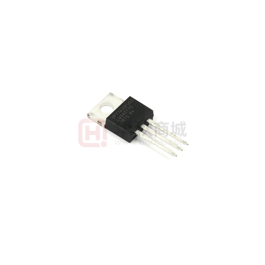
LM340, LM340A, LM7805, LM7812, LM7815
SNOSBT0L – FEBRUARY 2000 – REVISED SEPTEMBER 2016
LM340, LM340A and LM7805 Family Wide VIN 1.5-A Fixed Voltage Regulators
1 Features
3 Description
•
•
•
The LM340 and LM7805 Family monolithic 3-terminal
positive voltage regulators employ internal currentlimiting,
thermal
shutdown
and
safe-area
compensation, making them essentially indestructible.
If adequate heat sinking is provided, they can deliver
over 1.5-A output current. They are intended as fixed
voltage regulators in a wide range of applications
including local (on-card) regulation for elimination of
noise and distribution problems associated with
single-point regulation. In addition to use as fixed
voltage regulators, these devices can be used with
external components to obtain adjustable output
voltages and currents.
1
•
•
•
•
•
Output Current up to 1.5 A
Available in Fixed 5-V, 12-V, and 15-V Options
Output Voltage Tolerances of ±2% at TJ = 25°C
(LM340A)
Line Regulation of 0.01% / V of at 1-A Load
(LM340A)
Load Regulation of 0.3% / A (LM340A)
Internal Thermal Overload, Short-Circuit and SOA
Protection
Available in Space-Saving SOT-223 Package
Output Capacitance Not Required for Stability
Considerable effort was expended to make the entire
series of regulators easy to use and minimize the
number of external components. It is not necessary to
bypass the output, although this does improve
transient response. Input bypassing is needed only if
the regulator is located far from the filter capacitor of
the power supply.
2 Applications
•
•
•
•
•
•
•
Industrial Power Supplies
SMPS Post Regulation
HVAC Systems
AC Inventors
Test and Measurement Equipment
Brushed and Brushless DC Motor Drivers
Solar Energy String Invertors
SPACE
LM7805 is also available in a higher accuracy and
better performance version (LM340A). Refer to
LM340A specifications in the LM340A Electrical
Characterisitcs table.
Device Information(1)
Available Packages
PART NUMBER
Pin 1. Input
2. Ground
3. Output
2
Tab/Case is Ground or Output
LM340x
LM7805 Family
1
TO-3
TO-220
1
2
PACKAGE
BODY SIZE (NOM)
DDPAK/TO-263 (3)
10.18 mm × 8.41 mm
SOT-223 (4)
6.50 mm × 3.50 mm
TO-220 (3)
14.986 mm × 10.16 mm
TO-3 (2)
38.94 mm x 25.40 mm
(1) For all available packages, see the orderable addendum at
the end of the data sheet.
3
Fixed Output Voltage Regulator
TO-263
1 2
3
SOT-223
1
2 3
*Required if the regulator is located far from
the power supply filter.
**Although no output capacitor is needed
for stability, it does help transient response.
(If needed, use 0.1-μF, ceramic disc).
1
An IMPORTANT NOTICE at the end of this data sheet addresses availability, warranty, changes, use in safety-critical applications,
intellectual property matters and other important disclaimers. PRODUCTION DATA.
�LM340, LM340A, LM7805, LM7812, LM7815
SNOSBT0L – FEBRUARY 2000 – REVISED SEPTEMBER 2016
www.ti.com
Table of Contents
1
2
3
4
5
6
7
Features ..................................................................
Applications ...........................................................
Description .............................................................
Revision History.....................................................
Pin Configuration and Functions .........................
Specifications.........................................................
1
1
1
2
3
4
6.1 Absolute Maximum Ratings ......................................
6.2 ESD Ratings..............................................................
6.3 Recommended Operating Conditions.......................
6.4 Thermal Information ..................................................
6.5 LM340A Electrical Characteristics,
VO = 5 V, VI = 10 V............................................................
6.6 LM340 / LM7805 Electrical Characteristics,
VO = 5 V, VI = 10 V............................................................
6.7 LM340 / LM7812 Electrical Characteristics,
VO = 12 V, VI = 19 V..........................................................
6.8 LM340 / LM7815 Electrical Characteristics,
VO = 15 V, VI = 23 V..........................................................
6.9 Typical Characteristics ..............................................
4
4
4
4
5
6
7
8
9
Detailed Description ............................................ 12
7.1 Overview ................................................................. 12
7.2 Functional Block Diagram ....................................... 12
7.3 Feature Description................................................. 12
7.4 Device Functional Modes........................................ 12
8
Application and Implementation ........................ 13
8.1 Application Information............................................ 13
8.2 Typical Applications ................................................ 14
8.3 System Examples ................................................... 15
9 Power Supply Recommendations...................... 17
10 Layout................................................................... 17
10.1 Layout Guidelines ................................................. 17
10.2 Layout Example ................................................... 17
10.3 Heat Sinking DDPAK/TO-263 and SOT-223
Package Parts.......................................................... 18
11 Device and Documentation Support ................. 20
11.1
11.2
11.3
11.4
11.5
11.6
11.7
Documentation Support ........................................
Related Links ........................................................
Receiving Notification of Documentation Updates
Community Resources..........................................
Trademarks ...........................................................
Electrostatic Discharge Caution ............................
Glossary ................................................................
20
20
20
20
20
20
20
12 Mechanical, Packaging, and Orderable
Information ........................................................... 21
4 Revision History
NOTE: Page numbers for previous revisions may differ from page numbers in the current version.
Changes from Revision K (November 2015) to Revision L
•
Page
Changed pinout number order for the TO-220 and SOT-223 packages from: 2, 3, 1 to: 1, 2, 3 .......................................... 1
Changes from Revision J (December 2013) to Revision K
Page
•
Added ESD Ratings table, Thermal Information table, Feature Description section, Device Functional Modes,
Application and Implementation section, Power Supply Recommendations section, Layout section, Device and
Documentation Support section, and Mechanical, Packaging, and Orderable Information section....................................... 1
•
Deleted obsolete LM140 and LM7808C devices from the data sheet ................................................................................... 1
•
Changed Figure 13 caption from Line Regulation 140AK-5.0 to Line Regulation LM340, .................................................. 11
•
Changed Figure 14 caption from Line Regulation 140AK-5.0 to Line Regulation LM340, .................................................. 11
Changes from Revision I (March 2013) to Revision J
•
2
Page
Changed 0.5 from typ to max ................................................................................................................................................. 5
Submit Documentation Feedback
Copyright © 2000–2016, Texas Instruments Incorporated
Product Folder Links: LM340 LM340A LM7805 LM7812 LM7815
�LM340, LM340A, LM7805, LM7812, LM7815
www.ti.com
SNOSBT0L – FEBRUARY 2000 – REVISED SEPTEMBER 2016
5 Pin Configuration and Functions
LM7805 and LM7812 KTT Package
3-Pin DDPAK/TO-263
Top View
LM7805 DCY Package
4-Pin SOT-223
Side View
LM340K-5.0 NDS Package
2-Pin TO-3
Top View
LM7805, LM7812, and LM7815 NDE Package
3-Pin TO-220
Top View
Pin Functions
PIN
I/O
DESCRIPTION
NAME
NO.
INPUT
1
I
GND
2
I/O
Ground pin
OUTPUT
3
O
Output voltage pin
Input voltage pin
Copyright © 2000–2016, Texas Instruments Incorporated
Submit Documentation Feedback
Product Folder Links: LM340 LM340A LM7805 LM7812 LM7815
3
�LM340, LM340A, LM7805, LM7812, LM7815
SNOSBT0L – FEBRUARY 2000 – REVISED SEPTEMBER 2016
www.ti.com
6 Specifications
6.1 Absolute Maximum Ratings
over operating free-air temperature range (unless otherwise noted) (1) (2)
MIN
DC input voltage
Internal power dissipation
(3)
Lead temperature (soldering, 10 sec.)
TO-3 package (NDS)
Lead temperature 1,6 mm (1/16 in) from case for 10 s
−65
Storage temperature
(2)
(3)
UNIT
35
V
Internally Limited
Maximum junction temperature
(1)
MAX
150
°C
300
°C
230
°C
150
°C
Stresses beyond those listed under Absolute Maximum Ratings may cause permanent damage to the device. These are stress ratings
only, which do not imply functional operation of the device at these or any other conditions beyond those indicated under Recommended
Operating Conditions. Exposure to absolute-maximum-rated conditions for extended periods may affect device reliability.
If Military/Aerospace specified devices are required, please contact the Texas Instruments Sales Office/Distributors for availability and
specifications.
The maximum allowable power dissipation at any ambient temperature is a function of the maximum junction temperature for operation
(TJMAX = 125°C or 150°C), the junction-to-ambient thermal resistance (θJA), and the ambient temperature (TA). PDMAX = (TJMAX −
TA)/θJA. If this dissipation is exceeded, the die temperature rises above TJMAX and the electrical specifications do not apply. If the die
temperature rises above 150°C, the device goes into thermal shutdown. For the TO-3 package (NDS), the junction-to-ambient thermal
resistance (θJA) is 39°C/W. When using a heat sink, θJA is the sum of the 4°C/W junction-to-case thermal resistance (θJC) of the TO-3
package and the case-to-ambient thermal resistance of the heat sink. For the TO-220 package (NDE), θJA is 54°C/W and θJC is 4°C/W.
If SOT-223 is used, the junction-to-ambient thermal resistance is 174°C/W and can be reduced by a heat sink (see Applications Hints on
heat sinking).If the DDPAK\TO-263 package is used, the thermal resistance can be reduced by increasing the PCB copper area
thermally connected to the package: Using 0.5 square inches of copper area, θJA is 50°C/W; with 1 square inch of copper area, θJA is
37°C/W; and with 1.6 or more inches of copper area, θJA is 32°C/W.
6.2 ESD Ratings
V(ESD)
(1)
Electrostatic
discharge
Human-body model (HBM)
(1)
VALUE
UNIT
±2000
V
ESD rating is based on the human-body model, 100 pF discharged through 1.5 kΩ.
6.3 Recommended Operating Conditions
over operating free-air temperature range (unless otherwise noted)
Temperature (TA)
MIN
MAX
UNIT
0
125
°C
LM340A, LM340
6.4 Thermal Information
LM340, LM7805 Family
THERMAL METRIC (1)
RθJA
KTT
(DDPAK/TO-263)
DCY
(SOT-223)
NDS
(TO-3)
3 PINS
3 PINS
4 PINS
2 PINS
UNIT
23.9
44.8
62.1
39
°C/W
RθJC(top) Junction-to-case (top) thermal resistance
16.7
45.6
44
2
°C/W
RθJB
Junction-to-board thermal resistance
5.3
24.4
10.7
—
°C/W
ψJT
Junction-to-top characterization parameter
3.2
11.2
2.7
—
°C/W
ψJB
Junction-to-board characterization parameter
5.3
23.4
10.6
—
°C/W
RθJC(bot) Junction-to-case (bottom) thermal resistance
1.7
1.5
—
—
°C/W
(1)
4
Junction-to-ambient thermal resistance
NDE
(TO-220)
For more information about traditional and new thermal metrics, see the Semiconductor and IC Package Thermal Metrics application
report.
Submit Documentation Feedback
Copyright © 2000–2016, Texas Instruments Incorporated
Product Folder Links: LM340 LM340A LM7805 LM7812 LM7815
�LM340, LM340A, LM7805, LM7812, LM7815
www.ti.com
SNOSBT0L – FEBRUARY 2000 – REVISED SEPTEMBER 2016
6.5 LM340A Electrical Characteristics,
VO = 5 V, VI = 10 V
IOUT = 1 A, 0°C ≤ TJ ≤ 125°C (LM340A) unless otherwise specified (1)
PARAMETER
VO
TEST CONDITIONS
Output voltage
MIN
TYP
MAX
TJ = 25°C
4.9
5
5.1
PD ≤ 15 W, 5 mA ≤ IO ≤ 1 A
4.8
UNIT
V
5.2
V
7.5 V ≤ VIN ≤ 20 V
7.5 V ≤ VIN ≤ 20
V
ΔVO
Line regulation
8 V ≤ VIN ≤ 12 V
ΔVO
TJ = 25°C
Load regulation
TJ = 25°C
3
Over temperature, IO = 500 mA
TJ = 25°C
Over temperature
5 mA ≤ IO ≤ 1.5 A
10
250 mA ≤ IO ≤ 750 mA
Over temperature, 5 mA ≤ IO ≤ 1 A
IQ
TJ = 25°C
Quiescent current
10
mV
10
mV
4
mV
12
mV
25
mV
15
mV
25
mV
6
mA
Over temperature
6.5
mA
TJ = 25°C, IO = 1 A
0.8
7.5 V ≤ VIN ≤ 20 V
ΔIQ
Quiescent current
change
Over temperature, 5 mA ≤ IO ≤ 1 A
0.5
Over temperature, IO = 500 mA
0.8
8 V ≤ VIN ≤ 25 V
VN
TA = 25°C, 10 Hz ≤ f ≤ 100 kHz
Output noise voltage
f = 120 Hz
8 V ≤ VIN ≤ 18
Over temperature, IO = 500 mA
V
Ripple rejection
RO
VIN
(1)
TJ = 25°C, , IO = 1 A
68
mA
mA
mA
40
μV
80
dB
68
dB
Dropout voltage
TJ = 25°C, IO = 1 A
2
V
Output resistance
f = 1 kHz
8
mΩ
Short-circuit current
TJ = 25°C
2.1
Peak output current
TJ = 25°C
2.4
Average TC of VO
Min, TJ = 0°C, IO = 5 mA
Input voltage required to
maintain line regulation
TJ = 25°C
−0.6
A
A
mV/°C
7.5
V
All characteristics are measured with a 0.22-μF capacitor from input to ground and a 0.1-μF capacitor from output to ground. All
characteristics except noise voltage and ripple rejection ratio are measured using pulse techniques (tw ≤ 10 ms, duty cycle ≤ 5%).
Output voltage changes due to changes in internal temperature must be taken into account separately.
Copyright © 2000–2016, Texas Instruments Incorporated
Submit Documentation Feedback
Product Folder Links: LM340 LM340A LM7805 LM7812 LM7815
5
�LM340, LM340A, LM7805, LM7812, LM7815
SNOSBT0L – FEBRUARY 2000 – REVISED SEPTEMBER 2016
www.ti.com
6.6 LM340 / LM7805 Electrical Characteristics,
VO = 5 V, VI = 10 V
0°C ≤ TJ ≤ 125°C unless otherwise specified (1)
PARAMETER
VO
TEST CONDITIONS
Output voltage
MIN
TYP
MAX
TJ = 25°C, 5 mA ≤ IO ≤ 1 A
4.8
5
5.2
PD ≤ 15 W, 5 mA ≤ IO ≤ 1 A
4.75
UNIT
V
5.25
V
7.5 V ≤ VIN ≤ 20 V
TJ = 25°C
IO = 500 mA
ΔVO
3
50
7V ≤ VIN ≤ 25V
Over temperature
50
8V ≤ VIN ≤ 20V
Line regulation
TJ = 25°C
IO ≤ 1 A
50
7.5V ≤ VIN ≤ 20V
Over temperature
25
8V ≤ VIN ≤ 12V
ΔVO
TJ = 25°C
Load regulation
5 mA ≤ IO ≤ 1.5 A
10
250 mA ≤ IO ≤ 750 mA
Over temperature, 5 mA ≤ IO ≤ 1 A
IQ
IO ≤ 1 A
Quiescent current
TJ = 25°C
Over temperature
0°C ≤ TJ ≤ 125°C, 5 mA ≤ IO ≤ 1 A
ΔIQ
VN
Quiescent current change
f = 120 Hz
VIN
(1)
6
mV
50
mV
8
mA
8.5
mA
mA
Over temperature, IO ≤ 500
mA
1
Over temperature, IO ≤ 500
8 V ≤ VIN ≤ 18 V mA
mV
25
1
62
mV
mV
TJ = 25°C, IO ≤ 1 A
TJ = 25°C, IO ≤ 1 A
mV
50
0.5
TA = 25°C, 10 Hz ≤ f ≤ 100 kHz
Output noise voltage
Ripple rejection
RO
7 V ≤ VIN ≤ 20 V
mV
mA
mA
40
μV
80
dB
62
dB
Dropout voltage
TJ = 25°C, IO = 1 A
2
V
Output resistance
f = 1 kHz
8
mΩ
Short-circuit current
TJ = 25°C
2.1
Peak output current
TJ = 25°C
2.4
Average TC of VOUT
Over temperature, IO = 5 mA
Input voltage required to
maintain line regulation
TJ = 25°C, IO ≤ 1 A
−0.6
A
A
mV/°C
7.5
V
All characteristics are measured with a 0.22-μF capacitor from input to ground and a 0.1-μF capacitor from output to ground. All
characteristics except noise voltage and ripple rejection ratio are measured using pulse techniques (tw ≤ 10 ms, duty cycle ≤ 5%).
Output voltage changes due to changes in internal temperature must be taken into account separately.
Submit Documentation Feedback
Copyright © 2000–2016, Texas Instruments Incorporated
Product Folder Links: LM340 LM340A LM7805 LM7812 LM7815
�LM340, LM340A, LM7805, LM7812, LM7815
www.ti.com
SNOSBT0L – FEBRUARY 2000 – REVISED SEPTEMBER 2016
6.7 LM340 / LM7812 Electrical Characteristics,
VO = 12 V, VI = 19 V
0°C ≤ TJ ≤ 125°C unless otherwise specified (1)
PARAMETER
VO
TEST CONDITIONS
Output voltage
MIN
TYP
MAX
UNIT
TJ = 25°C, 5 mA ≤ IO ≤ 1 A
11.5
12
12.5
V
PD ≤ 15 W, 5 mA ≤ IO ≤ 1 A
11.4
12.6
V
14.5 V ≤ VIN ≤ 27 V
TJ = 25°C
IO = 500 mA
ΔVO
4
120
mV
14.5V ≤ VIN ≤ 30V
Over temperature
120
mV
15V ≤ VIN ≤ 27V
Line regulation
TJ = 25°C
IO ≤ 1 A
120
mV
14.6V ≤ VIN ≤ 27V
Over temperature
60
mV
16V ≤ VIN ≤ 22V
ΔVO
TJ = 25°C
Load regulation
5 mA ≤ IO ≤ 1.5 A
12
250 mA ≤ IO ≤ 750 mA
Over temperature, 5 mA ≤ IO ≤ 1 A
IQ
IO ≤ 1 A
Quiescent current
TJ = 25°C
Over temperature
5 mA ≤ IO ≤ 1 A
Quiescent current change
mV
60
mV
120
mV
8
mA
8.5
mA
0.5
TJ = 25°C, IO ≤ 1 A
ΔIQ
120
mA
1
mA
14.8 V ≤ VIN ≤ 27 V
Over temperature, IO ≤ 500 mA
1
mA
14.5 V ≤ VIN ≤ 30 V
VN
Output noise voltage
TA = 25°C, 10 Hz ≤ f ≤ 100 kHz
f = 120 Hz
RO
VIN
(1)
TJ = 25°C, IO ≤ 1 A
Ripple rejection
15 V ≤ VIN ≤ 25 Over temperature, IO ≤ 500
mA,
V
Dropout voltage
TJ = 25°C, IO = 1 A
Output resistance
Short-circuit current
55
75
μV
72
dB
55
dB
2
V
f = 1 kHz
18
mΩ
TJ = 25°C
1.5
A
Peak output current
TJ = 25°C
2.4
Average TC of VOUT
Over temperature, IO = 5 mA
Input voltage required to
maintain line regulation
TJ = 25°C, IO ≤ 1 A
−1.5
A
mV/°C
14.6
V
All characteristics are measured with a 0.22-μF capacitor from input to ground and a 0.1-μF capacitor from output to ground. All
characteristics except noise voltage and ripple rejection ratio are measured using pulse techniques (tw ≤ 10 ms, duty cycle ≤ 5%).
Output voltage changes due to changes in internal temperature must be taken into account separately.
Copyright © 2000–2016, Texas Instruments Incorporated
Submit Documentation Feedback
Product Folder Links: LM340 LM340A LM7805 LM7812 LM7815
7
�LM340, LM340A, LM7805, LM7812, LM7815
SNOSBT0L – FEBRUARY 2000 – REVISED SEPTEMBER 2016
www.ti.com
6.8 LM340 / LM7815 Electrical Characteristics,
VO = 15 V, VI = 23 V
0°C ≤ TJ ≤ 125°C unless otherwise specified (1)
PARAMETER
VO
TEST CONDITIONS
Output voltage
MIN
TYP
MAX
UNIT
TJ = 25°C, 5 mA ≤ IO ≤ 1 A
14.4
15
15.6
V
PD ≤ 15 W, 5 mA ≤ IO ≤ 1 A
14.25
15.75
V
17.5 V ≤ VIN ≤ 30 V
TJ = 25°C
IO = 500 mA
ΔVO
4
150
17.5 V ≤ VIN ≤ 30 V
Over temperature
150
18.5 V ≤ VIN ≤ 30 V
Line regulation
TJ = 25°C
IO ≤ 1 A
150
17.7 V ≤ VIN ≤ 30 V
Over temperature
75
20 V ≤ VIN ≤ 26 V
ΔVO
TJ = 25°C
Load regulation
5 mA ≤ IO ≤ 1.5 A
12
250 mA ≤ IO ≤ 750 mA
Over temperature, 5 mA ≤ IO ≤ 1 A,
IQ
IO ≤ 1 A
Quiescent current
TJ = 25°C
Over temperature
5 mA ≤ IO ≤ 1 A
ΔIQ
Quiescent current change
VN
f = 120 Hz
RO
VIN
(1)
8
75
mV
mV
8
mA
8.5
mA
mA
1
TA = 25°C, 10 Hz ≤ f ≤ 100 kHz
Output noise voltage
TJ = 25°C, IO ≤ 1 A
Ripple rejection
18.5 V ≤ VIN ≤ Over temperature, IO ≤ 500
mA,
28.5 V
Dropout voltage
TJ = 25°C, IO = 1 A
Output resistance
Short-circuit current
54
mV
150
17.9 V ≤ VIN ≤ 30 V
17.5 V ≤ VIN ≤ 30 V
mV
mV
1
Over temperature, IO ≤ 500 mA
mV
150
0.5
TJ = 25°C, IO ≤ 1 A
mV
mA
mA
90
μV
70
dB
54
dB
2
V
f = 1 kHz
19
mΩ
TJ = 25°C
1.2
A
Peak output current
TJ = 25°C
2.4
Average TC of VOUT
Over temperature, IO = 5 mA
Input voltage required to
maintain line regulation
TJ = 25°C, IO ≤ 1 A
−1.8
A
mV/°C
17.7
V
All characteristics are measured with a 0.22-μF capacitor from input to ground and a 0.1-μF capacitor from output to ground. All
characteristics except noise voltage and ripple rejection ratio are measured using pulse techniques (tw ≤ 10 ms, duty cycle ≤ 5%).
Output voltage changes due to changes in internal temperature must be taken into account separately.
Submit Documentation Feedback
Copyright © 2000–2016, Texas Instruments Incorporated
Product Folder Links: LM340 LM340A LM7805 LM7812 LM7815
�LM340, LM340A, LM7805, LM7812, LM7815
www.ti.com
SNOSBT0L – FEBRUARY 2000 – REVISED SEPTEMBER 2016
6.9 Typical Characteristics
Figure 1. Maximum Average Power Dissipation
Figure 3. Maximum Power Dissipation (DDPAK/TO-263)
Figure 5. Ripple Rejection
Copyright © 2000–2016, Texas Instruments Incorporated
Figure 2. Maximum Average Power Dissipation
Shaded area refers to LM340A/LM340, LM7805, LM7812 and
LM7815.
Figure 4. Output Voltage (Normalized to 1 V at TJ = 25°C)
Figure 6. Ripple Rejection
Submit Documentation Feedback
Product Folder Links: LM340 LM340A LM7805 LM7812 LM7815
9
�LM340, LM340A, LM7805, LM7812, LM7815
SNOSBT0L – FEBRUARY 2000 – REVISED SEPTEMBER 2016
www.ti.com
Typical Characteristics (continued)
Figure 7. Output Impedance
Figure 8. Dropout Characteristics
Shaded area refers to LM340A/LM340, LM7805, LM7812, and
LM7815.
Figure 9. Quiescent Current
Figure 10. Peak Output Current
Shaded area refers to LM340A/LM340, LM7805, LM7812, and
LM7815.
Figure 11. Dropout Voltage
Figure 12. Quiescent Current
10
Submit Documentation Feedback
Copyright © 2000–2016, Texas Instruments Incorporated
Product Folder Links: LM340 LM340A LM7805 LM7812 LM7815
�LM340, LM340A, LM7805, LM7812, LM7815
www.ti.com
SNOSBT0L – FEBRUARY 2000 – REVISED SEPTEMBER 2016
Typical Characteristics (continued)
IOUT = 1 A, TA = 25°C
Figure 13. Line Regulation LM340
Copyright © 2000–2016, Texas Instruments Incorporated
VIN = 10 V, TA = 25°C
Figure 14. Line Regulation LM340
Submit Documentation Feedback
Product Folder Links: LM340 LM340A LM7805 LM7812 LM7815
11
�LM340, LM340A, LM7805, LM7812, LM7815
SNOSBT0L – FEBRUARY 2000 – REVISED SEPTEMBER 2016
www.ti.com
7 Detailed Description
7.1 Overview
The LM340 and LM7805 devices are a family of fixed output positive voltage regulators with outputs ranging from
3 V to 15 V. They accept up to 35 V of input voltage and with proper heat dissipation can provide over 1.5 A of
current. With a combination of current limiting, thermal shutdown, and safe area protection, these regulators
eliminate any concern of damage. These features paired with excellent line and load regulation make the LM340
and LM7805 Family versatile solutions to a wide range of power management designs. Although the LM340 and
LM7805 Family were designed primarily as fixed-voltage regulators, these devices can be used with external
component for adjustable voltage and current.
7.2 Functional Block Diagram
7.3 Feature Description
7.3.1 Output Current
With proper considerations, the LM340 and LM7805 Family can exceed 1.5-A output current. Depending on the
desired package option, the effective junction-to-ambient thermal resistance can be reduced through heat
sinking, allowing more power to be dissipated in the device.
7.3.2 Current Limiting Feature
In the event of a short circuit at the output of the regulator, each device has an internal current limit to protect it
from damage. The typical current limits for the LM340 and LM7805 Family is 2.4 A.
7.3.3 Thermal Shutdown
Each package type employs internal current limiting and thermal shutdown to provide safe operation area
protection. If the junction temperature is allowed to rise to 150°C, the device will go into thermal shutdown.
7.4 Device Functional Modes
There are no functional modes for this device.
12
Submit Documentation Feedback
Copyright © 2000–2016, Texas Instruments Incorporated
Product Folder Links: LM340 LM340A LM7805 LM7812 LM7815
�LM340, LM340A, LM7805, LM7812, LM7815
www.ti.com
SNOSBT0L – FEBRUARY 2000 – REVISED SEPTEMBER 2016
8 Application and Implementation
NOTE
Information in the following applications sections is not part of the TI component
specification, and TI does not warrant its accuracy or completeness. TI’s customers are
responsible for determining suitability of components for their purposes. Customers should
validate and test their design implementation to confirm system functionality.
8.1 Application Information
The LM340x and LM7805 series is designed with thermal protection, output short-circuit protection, and output
transistor safe area protection. However, as with any IC regulator, it becomes necessary to take precautions to
assure that the regulator is not inadvertently damaged. The following describes possible misapplications and
methods to prevent damage to the regulator.
8.1.1 Shorting the Regulator Input
When using large capacitors at the output of these regulators, a protection diode connected input to output
(Figure 15) may be required if the input is shorted to ground. Without the protection diode, an input short causes
the input to rapidly approach ground potential, while the output remains near the initial VOUT because of the
stored charge in the large output capacitor. The capacitor will then discharge through a large internal input to
output diode and parasitic transistors. If the energy released by the capacitor is large enough, this diode, low
current metal, and the regulator are destroyed. The fast diode in Figure 15 shunts most of the capacitors
discharge current around the regulator. Generally no protection diode is required for values of output capacitance
≤ 10 μF.
8.1.2 Raising the Output Voltage Above the Input Voltage
Because the output of the device does not sink current, forcing the output high can cause damage to internal low
current paths in a manner similar to that just described in Shorting the Regulator Input.
8.1.3 Regulator Floating Ground
When the ground pin alone becomes disconnected, the output approaches the unregulated input, causing
possible damage to other circuits connected to VOUT. If ground is reconnected with power ON, damage may also
occur to the regulator. This fault is most likely to occur when plugging in regulators or modules with on card
regulators into powered up sockets. The power must be turned off first, the thermal limit ceases operating, or the
ground must be connected first if power must be left on. See Figure 16.
8.1.4 Transient Voltages
If transients exceed the maximum rated input voltage of the device, or reach more than 0.8 V below ground and
have sufficient energy, they will damage the regulator. The solution is to use a large input capacitor, a series
input breakdown diode, a choke, a transient suppressor or a combination of these.
Figure 15. Input Short
Copyright © 2000–2016, Texas Instruments Incorporated
Submit Documentation Feedback
Product Folder Links: LM340 LM340A LM7805 LM7812 LM7815
13
�LM340, LM340A, LM7805, LM7812, LM7815
SNOSBT0L – FEBRUARY 2000 – REVISED SEPTEMBER 2016
www.ti.com
Application Information (continued)
Figure 16. Regulator Floating Ground
Figure 17. Transients
When a value for θ(H–A) is found, a heat sink must be selected that has a value that is less than or equal to this
number.
θ(H–A) is specified numerically by the heat sink manufacturer in this catalog or shown in a curve that plots
temperature rise vs power dissipation for the heat sink.
8.2 Typical Applications
8.2.1 Fixed Output Voltage Regulator
The LM340x and LM7805 Family devices are primarily designed to provide fixed output voltage regulation. The
simplest implementation of LM340x and LM7805 Family is shown in Figure 18.
*Required if the regulator is located far from the power supply filter.
**Although no output capacitor is needed for stability, it does help transient response. (If needed, use 0.1-μF, ceramic
disc).
Figure 18. Fixed Output Voltage Regulator
8.2.1.1 Design Requirements
The device component count is very minimal. Although not required, TI recommends employing bypass
capacitors at the output for optimum stability and transient response. These capacitors must be placed as close
as possible to the regulator. If the device is located more than 6 inches from the power supply filter, it is required
to employ input capacitor.
14
Submit Documentation Feedback
Copyright © 2000–2016, Texas Instruments Incorporated
Product Folder Links: LM340 LM340A LM7805 LM7812 LM7815
�LM340, LM340A, LM7805, LM7812, LM7815
www.ti.com
SNOSBT0L – FEBRUARY 2000 – REVISED SEPTEMBER 2016
Typical Applications (continued)
8.2.1.2 Detailed Design Procedure
The output voltage is set based on the device variant. LM340x and LM7805 Family are available in 5-V, 12-V
and 15-V regulator options.
8.2.1.3 Application Curve
Figure 19. VOUT vs VIN, VOUT = 5 V
8.3 System Examples
IOUT = V2–3 / R1 + IQ
ΔIQ = 1.3 mA over line and load changes.
VOUT = 5 V + (5 V/R1 + IQ) R2 5 V/R1 > 3 IQ,
load regulation (Lr) ≈ [(R1 + R2)/R1] (Lr of LM340-5).
Figure 20. Current Regulator
INPUT
Figure 21. Adjustable Output Regulator
OUTPUT
VI
VO
0.22 PF
GND
VI
INPUT
0.1 PF
Copyright © 2000–2016, Texas Instruments Incorporated
VO
GND
0.22 PF
Figure 22. High Input Voltage Circuit With Series
Resistor
OUTPUT
0.1 PF
Figure 23. High Input Voltage Circuit
implementation With Transistor
Submit Documentation Feedback
Product Folder Links: LM340 LM340A LM7805 LM7812 LM7815
15
�LM340, LM340A, LM7805, LM7812, LM7815
SNOSBT0L – FEBRUARY 2000 – REVISED SEPTEMBER 2016
www.ti.com
System Examples (continued)
RSC
Q1
2N6133
IQ1
Q1
2N6132
IN
VI
R1
3.0:
Q2
2N6124
IREG
IO MAX
OUTPUT
VO
INPUT
0.22 PF
INPUT
OUT
GND
OUTPUT
R1
3.0:
0.1 PF
β(Q1) ≥ IO Max / IREG Max
R1 = 0.9 / IREG = β(Q1) VBE(Q1) / IREG Max (β +1) – IO Max
0.22 PF
GND
0.1 PF
RSC = 0.8 / ISC
R1 = βVBE(Q1) / IREG Max (β +1) – IO Max
Figure 24. High Current Voltage Regulator
Figure 25. High Output Current With Short-Circuit
Protection
INPUT
OUTPUT
+ OUT
LM340
+
+
0.1 PF
GND
INPUT
OUTPUT
LM79xx
+
+
GND
0.1 PF
- OUT
Figure 26. LM340 Used With Negative Regulator LM79xx
16
Submit Documentation Feedback
Copyright © 2000–2016, Texas Instruments Incorporated
Product Folder Links: LM340 LM340A LM7805 LM7812 LM7815
�LM340, LM340A, LM7805, LM7812, LM7815
www.ti.com
SNOSBT0L – FEBRUARY 2000 – REVISED SEPTEMBER 2016
9 Power Supply Recommendations
The LM340 is designed to operate from a wide input voltage up to 35 V. Please refer to electrical characteristics
tables for the minimum input voltage required for line/load regulation. If the device is more than six inches from
the input filter capacitors, an input bypass capacitor, 0.1 μF or greater, of any type is needed for stability.
10 Layout
10.1 Layout Guidelines
Some layout guidelines must be followed to ensure proper regulation of the output voltage with minimum noise.
Traces carrying the load current must be wide to reduce the amount of parasitic trace inductance. To improve
PSRR, a bypass capacitor can be placed at the OUTPUT pin and must be placed as close as possible to the IC.
All that is required for the typical fixed output regulator application circuit is the LM340x/LM7805 Family IC and a
0.22-µF input capacitor if the regulator is placed far from the power supply filter. A 0.1-µF output capacitor is
recommended to help with transient response. In cases when VIN shorts to ground, an external diode must be
placed from VOUT to VIN to divert the surge current from the output capacitor and protect the IC.
10.2 Layout Example
Figure 27. Layout Example DDPAK
Copyright © 2000–2016, Texas Instruments Incorporated
Submit Documentation Feedback
Product Folder Links: LM340 LM340A LM7805 LM7812 LM7815
17
�LM340, LM340A, LM7805, LM7812, LM7815
SNOSBT0L – FEBRUARY 2000 – REVISED SEPTEMBER 2016
www.ti.com
Layout Example (continued)
Figure 28. Layout Example SOT-223
10.3 Heat Sinking DDPAK/TO-263 and SOT-223 Package Parts
Both the DDPAK/TO-263 (KTT) and SOT-223 (DCY) packages use a copper plane on the PCB and the PCB
itself as a heat sink. To optimize the heat sinking ability of the plane and PCB, solder the tab of the plane.
Figure 29 shows for the DDPAK/TO-263 the measured values of θ(J–A) for different copper area sizes using a
typical PCB with 1-oz copper and no solder mask over the copper area used for heat sinking.
Figure 29. θ(J–A) vs Copper (1 Ounce) Area for the DDPAK/TO-263 Package
18
Submit Documentation Feedback
Copyright © 2000–2016, Texas Instruments Incorporated
Product Folder Links: LM340 LM340A LM7805 LM7812 LM7815
�LM340, LM340A, LM7805, LM7812, LM7815
www.ti.com
SNOSBT0L – FEBRUARY 2000 – REVISED SEPTEMBER 2016
Heat Sinking DDPAK/TO-263 and SOT-223 Package Parts (continued)
As shown in Figure 29, increasing the copper area beyond 1 square inch produces very little improvement. It
should also be observed that the minimum value of θ(J–A) for the DDPAK/TO-263 package mounted to a PCB is
32°C/W.
As a design aid, Figure 30 shows the maximum allowable power dissipation compared to ambient temperature
for the DDPAK/TO-263 device (assuming θ(J–A) is 35°C/W and the maximum junction temperature is 125°C).
Figure 30. Maximum Power Dissipation vs TAMB for the DDPAK/TO-263 Package
Figure 31 and Figure 32 show the information for the SOT-223 package. Figure 31 assumes a θ(J–A) of 74°C/W
for 1-oz. copper and 51°C/W for 2-oz. copper and a maximum junction temperature of 125°C.
Figure 31. θ(J–A) vs Copper (2 Ounce) Area
for the SOT-223 Package
Figure 32. Maximum Power Dissipation vs
TAMB for the SOT-223 Package
See AN-1028 LMX2370 PLLatinum Dual Freq Synth for RF Pers Comm LMX2370 2.5GHz/1.2GHz (SNVA036)
for power enhancement techniques to be used with the SOT-223 package.
Copyright © 2000–2016, Texas Instruments Incorporated
Submit Documentation Feedback
Product Folder Links: LM340 LM340A LM7805 LM7812 LM7815
19
�LM340, LM340A, LM7805, LM7812, LM7815
SNOSBT0L – FEBRUARY 2000 – REVISED SEPTEMBER 2016
www.ti.com
11 Device and Documentation Support
11.1 Documentation Support
11.1.1 Related Documentation
For related documentation, see the following:
• AN-1028 LMX2370 PLLatinum Dual Freq Synth for RF Pers Comm LMX2370 2.5GHz/1.2GHz (SNVA036)
• LM140K Series 3-Terminal Positive Regulators (SNVS994)
11.2 Related Links
The table below lists quick access links. Categories include technical documents, support and community
resources, tools and software, and quick access to sample or buy.
Table 1. Related Links
PARTS
PRODUCT FOLDER
SAMPLE & BUY
TECHNICAL
DOCUMENTS
TOOLS &
SOFTWARE
SUPPORT &
COMMUNITY
LM340
Click here
Click here
Click here
Click here
Click here
LM340A
Click here
Click here
Click here
Click here
Click here
LM7805
Click here
Click here
Click here
Click here
Click here
LM7812
Click here
Click here
Click here
Click here
Click here
LM7815
Click here
Click here
Click here
Click here
Click here
11.3 Receiving Notification of Documentation Updates
To receive notification of documentation updates, navigate to the device product folder on ti.com. In the upper
right corner, click on Alert me to register and receive a weekly digest of any product information that has
changed. For change details, review the revision history included in any revised document.
11.4 Community Resources
The following links connect to TI community resources. Linked contents are provided "AS IS" by the respective
contributors. They do not constitute TI specifications and do not necessarily reflect TI's views; see TI's Terms of
Use.
TI E2E™ Online Community TI's Engineer-to-Engineer (E2E) Community. Created to foster collaboration
among engineers. At e2e.ti.com, you can ask questions, share knowledge, explore ideas and help
solve problems with fellow engineers.
Design Support TI's Design Support Quickly find helpful E2E forums along with design support tools and
contact information for technical support.
11.5 Trademarks
E2E is a trademark of Texas Instruments.
All other trademarks are the property of their respective owners.
11.6 Electrostatic Discharge Caution
These devices have limited built-in ESD protection. The leads should be shorted together or the device placed in conductive foam
during storage or handling to prevent electrostatic damage to the MOS gates.
11.7 Glossary
SLYZ022 — TI Glossary.
This glossary lists and explains terms, acronyms, and definitions.
20
Submit Documentation Feedback
Copyright © 2000–2016, Texas Instruments Incorporated
Product Folder Links: LM340 LM340A LM7805 LM7812 LM7815
�LM340, LM340A, LM7805, LM7812, LM7815
www.ti.com
SNOSBT0L – FEBRUARY 2000 – REVISED SEPTEMBER 2016
12 Mechanical, Packaging, and Orderable Information
The following pages include mechanical, packaging, and orderable information. This information is the most
current data available for the designated devices. This data is subject to change without notice and revision of
this document. For browser-based versions of this data sheet, refer to the left-hand navigation.
Copyright © 2000–2016, Texas Instruments Incorporated
Submit Documentation Feedback
Product Folder Links: LM340 LM340A LM7805 LM7812 LM7815
21
�PACKAGE OPTION ADDENDUM
www.ti.com
28-Apr-2022
PACKAGING INFORMATION
Orderable Device
Status
(1)
Package Type Package Pins Package
Drawing
Qty
Eco Plan
(2)
Lead finish/
Ball material
MSL Peak Temp
Op Temp (°C)
Device Marking
(3)
(4/5)
(6)
LM340AT-5.0
NRND
TO-220
NDE
3
45
Non-RoHS
& Green
Call TI
Level-1-NA-UNLIM
0 to 70
LM340AT
5.0 P+
LM340AT-5.0/NOPB
ACTIVE
TO-220
NDE
3
45
RoHS-Exempt
& Green
SN
Level-1-NA-UNLIM
0 to 125
LM340AT
5.0 P+
LM340K-5.0
ACTIVE
TO-3
NDS
2
50
Non-RoHS &
Non-Green
Call TI
Call TI
0 to 125
LM340K
-5.0 7805P+
LM340K-5.0/NOPB
ACTIVE
TO-3
NDS
2
50
RoHS & Green
Call TI
Level-1-NA-UNLIM
0 to 125
LM340K
-5.0 7805P+
LM340MP-5.0
NRND
SOT-223
DCY
4
1000
Non-RoHS
& Green
Call TI
Level-1-260C-UNLIM
0 to 70
N00A
LM340MP-5.0/NOPB
ACTIVE
SOT-223
DCY
4
1000
RoHS & Green
SN
Level-1-260C-UNLIM
0 to 125
N00A
LM340MPX-5.0/NOPB
ACTIVE
SOT-223
DCY
4
2000
RoHS & Green
SN
Level-1-260C-UNLIM
0 to 125
N00A
LM340S-12/NOPB
ACTIVE
DDPAK/
TO-263
KTT
3
45
RoHS-Exempt
& Green
SN
Level-3-245C-168 HR
0 to 125
LM340S
-12 P+
LM340S-5.0
NRND
DDPAK/
TO-263
KTT
3
45
Non-RoHS
& Green
Call TI
Level-3-235C-168 HR
0 to 70
LM340S
-5.0 P+
LM340S-5.0/NOPB
ACTIVE
DDPAK/
TO-263
KTT
3
45
RoHS-Exempt
& Green
SN
Level-3-245C-168 HR
0 to 125
LM340S
-5.0 P+
LM340SX-12/NOPB
ACTIVE
DDPAK/
TO-263
KTT
3
500
RoHS-Exempt
& Green
SN
Level-3-245C-168 HR
0 to 125
LM340S
-12 P+
LM340SX-5.0
NRND
DDPAK/
TO-263
KTT
3
500
Non-RoHS
& Green
Call TI
Level-3-235C-168 HR
0 to 70
LM340S
-5.0 P+
LM340SX-5.0/NOPB
ACTIVE
DDPAK/
TO-263
KTT
3
500
RoHS-Exempt
& Green
SN
Level-3-245C-168 HR
0 to 125
LM340S
-5.0 P+
LM340T-12
NRND
TO-220
NDE
3
45
Non-RoHS
& Green
Call TI
Level-1-NA-UNLIM
0 to 70
LM340T12
7812 P+
LM340T-12/NOPB
ACTIVE
TO-220
NDE
3
45
RoHS & Green
SN
Level-1-NA-UNLIM
LM340T-15
NRND
TO-220
NDE
3
45
Non-RoHS
& Green
Call TI
Level-1-NA-UNLIM
0 to 70
LM340T15
7815 P+
LM340T-15/NOPB
ACTIVE
TO-220
NDE
3
45
RoHS & Green
SN
Level-1-NA-UNLIM
0 to 125
LM340T15
7815 P+
Addendum-Page 1
LM340T12
7812 P+
Samples
�PACKAGE OPTION ADDENDUM
www.ti.com
28-Apr-2022
Orderable Device
Status
(1)
Package Type Package Pins Package
Drawing
Qty
Eco Plan
(2)
Lead finish/
Ball material
MSL Peak Temp
Op Temp (°C)
Device Marking
(3)
(4/5)
(6)
LM340T-5.0
NRND
TO-220
NDE
3
45
Non-RoHS
& Green
Call TI
Level-1-NA-UNLIM
0 to 70
LM340T5
7805 P+
LM340T-5.0/LF01
ACTIVE
TO-220
NDG
3
45
RoHS-Exempt
& Green
SN
Level-4-260C-72 HR
0 to 125
LM340T5
7805 P+
LM340T-5.0/NOPB
ACTIVE
TO-220
NDE
3
45
RoHS-Exempt
& Green
SN
Level-1-NA-UNLIM
0 to 125
LM340T5
7805 P+
LM7805CT
NRND
TO-220
NDE
3
45
Non-RoHS
& Green
Call TI
Level-1-NA-UNLIM
0 to 125
LM340T5
7805 P+
LM7805CT/NOPB
ACTIVE
TO-220
NDE
3
45
RoHS-Exempt
& Green
SN
Level-1-NA-UNLIM
0 to 125
LM340T5
7805 P+
LM7805MP/NOPB
ACTIVE
SOT-223
DCY
4
1000
RoHS & Green
SN
Level-1-260C-UNLIM
0 to 125
N00A
LM7805MPX/NOPB
ACTIVE
SOT-223
DCY
4
2000
RoHS & Green
SN
Level-1-260C-UNLIM
0 to 125
N00A
LM7805S/NOPB
ACTIVE
DDPAK/
TO-263
KTT
3
45
RoHS-Exempt
& Green
SN
Level-3-245C-168 HR
0 to 125
LM340S
-5.0 P+
LM7805SX/NOPB
ACTIVE
DDPAK/
TO-263
KTT
3
500
RoHS-Exempt
& Green
SN
Level-3-245C-168 HR
0 to 125
LM340S
-5.0 P+
LM7812CT/NOPB
ACTIVE
TO-220
NDE
3
45
RoHS & Green
SN
Level-1-NA-UNLIM
-40 to 125
LM7812S/NOPB
ACTIVE
DDPAK/
TO-263
KTT
3
45
RoHS-Exempt
& Green
SN
Level-3-245C-168 HR
0 to 125
LM340S
-12 P+
LM7812SX/NOPB
ACTIVE
DDPAK/
TO-263
KTT
3
500
RoHS-Exempt
& Green
SN
Level-3-245C-168 HR
0 to 125
LM340S
-12 P+
LM7815CT/NOPB
ACTIVE
TO-220
NDE
3
45
RoHS & Green
SN
Level-1-NA-UNLIM
0 to 125
LM340T15
7815 P+
LM340T12
7812 P+
(1)
The marketing status values are defined as follows:
ACTIVE: Product device recommended for new designs.
LIFEBUY: TI has announced that the device will be discontinued, and a lifetime-buy period is in effect.
NRND: Not recommended for new designs. Device is in production to support existing customers, but TI does not recommend using this part in a new design.
PREVIEW: Device has been announced but is not in production. Samples may or may not be available.
OBSOLETE: TI has discontinued the production of the device.
(2)
RoHS: TI defines "RoHS" to mean semiconductor products that are compliant with the current EU RoHS requirements for all 10 RoHS substances, including the requirement that RoHS substance
do not exceed 0.1% by weight in homogeneous materials. Where designed to be soldered at high temperatures, "RoHS" products are suitable for use in specified lead-free processes. TI may
reference these types of products as "Pb-Free".
Addendum-Page 2
Samples
�PACKAGE OPTION ADDENDUM
www.ti.com
28-Apr-2022
RoHS Exempt: TI defines "RoHS Exempt" to mean products that contain lead but are compliant with EU RoHS pursuant to a specific EU RoHS exemption.
Green: TI defines "Green" to mean the content of Chlorine (Cl) and Bromine (Br) based flame retardants meet JS709B low halogen requirements of