LM3420
LM3420-4.2, -8.2, -8.4, -12.6, -16.8 Lithium-Ion Battery Charge Controller
Literature Number: SNVS116C
�LM3420-4.2, -8.2, -8.4, -12.6, -16.8
Lithium-Ion Battery Charge Controller
General Description
The LM3420 series of controllers are monolithic integrated
circuits designed for charging and end-of-charge control for
Lithium-Ion rechargeable batteries. The LM3420 is available
in five fixed voltage versions for one through four cell charger
applications (4.2V, 8.2V/8.4V, 12.6V and 16.8V respectively).
Included in a very small package is an (internally compensated) op amp, a bandgap reference, an NPN output transistor, and voltage setting resistors. The amplifier’s inverting
input is externally accessible for loop frequency compensation. The output is an open-emitter NPN transistor capable of
driving up to 15 mA of output current into external circuitry.
A trimmed precision bandgap reference utilizes temperature
drift curvature correction for excellent voltage stability over
the operating temperature range. Available with an initial
tolerance of 0.5% for the A grade version, and 1% for the
standard version, the LM3420 allows for precision end-ofcharge control for Lithium-Ion rechargeable batteries.
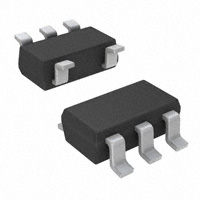
The LM3420 is available in a sub-miniature 5-lead SOT23-5
surface mount package thus allowing very compact designs.
Features
n
n
n
n
n
Voltage options for charging 1, 2, 3 or 4 cells
Tiny SOT23-5 package
Precision (0.5%) end-of-charge control
Drive capability for external power stage
Low quiescent current, 85 µA (typ.)
Applications
n Lithium-Ion battery charging
n Suitable for linear and switching regulator charger
designs
Typical Application and Functional Diagram
01235901
Typical Constant Current/Constant Voltage
Li-Ion Battery Charger
01235902
LM3420 Functional Diagram
SIMPLE SWITCHER ® is a registered trademark of National Semiconductor Corporation.
© 2004 National Semiconductor Corporation
DS012359
www.national.com
LM3420-4.2, -8.2, -8.4, -12.6, -16.8 Lithium-Ion Battery Charge Controller
July 2000
�LM3420-4.2/LM3420-8.2/LM3420-8.4/LM3420-12.6/LM3420-16.8
Connection Diagrams and Order Information
5-Lead Small Outline Package (M5)
Actual Size
01235904
01235903
*No internal connection, but should be soldered to PC board for best heat
transfer.
Top View
For Ordering Information See Figure 1 in this Data SheetSee NS Package Number MF05A
www.national.com
2
�ESD Susceptibility (Note 3)
Human Body Model
If Military/Aerospace specified devices are required,
please contact the National Semiconductor Sales Office/
Distributors for availability and specifications.
Input Voltage V(IN)
20V
Output Current
20 mA
Junction Temperature
150˚C
Storage Temperature
−65˚C to +150˚C
Operating Ratings (Notes 1, 2)
Lead Temperature
Vapor Phase (60 seconds)
+215˚C
Infrared (15 seconds)
+220˚C
Power Dissipation (TA = 25˚C)
(Note 2)
1500V
See AN-450 “Surface Mounting Methods and Their Effect
on Product Reliability” for methods on soldering
surface-mount devices.
Ambient Temperature Range
−40˚C ≤ TA ≤ +85˚C
Junction Temperature Range
−40˚C ≤ TJ ≤
+125˚C
Output Current
15 mA
300 mW
LM3420-4.2
Electrical Characteristics
Specifications with standard type face are for TJ = 25˚C, and those with boldface type apply over full Operating Temperature Range. Unless otherwise specified, V(IN) = VREG, VOUT = 1.5V.
Symbol
Parameter
Conditions
Typical
(Note 4)
VREG
Regulation Voltage
Regulation Voltage
IOUT = 1 mA
LM3420A-4.2
LM3420-4.2
Units
(Limits)
Limit
Limit
(Note 5)
(Note 5)
4.221/4.242
4.242/4.284
4.179/4.158
4.158/4.116
V(min)
± 0.5/ ± 1
± 1/ ± 2
%(max)
110/115
125/150
µA(max)
1.3/0.75
1.0/0.50
mA/mV(min)
3.0/1.5
2.5/1.4
mA/mV(min)
4.2
IOUT = 1 mA
V
V(max)
Tolerance
Iq
Gm
Quiescent Current
IOUT = 1 mA
Transconductance
20 µA ≤ IOUT ≤ 1 mA
∆IOUT/∆VREG
VOUT = 2V
85
3.3
1 mA ≤ IOUT ≤ 15 mA
Voltage Gain
∆VOUT/∆VREG
1V ≤ VOUT ≤ VREG − 1.2V (−1.3)
IL
Rf
Output Saturation
V(IN) = VREG +100 mV
IOUT = 15 mA
Output Leakage
V(IN) = VREG −100 mV
Current
VOUT = 0V
450/200
V/V(min)
1500/900
1000/700
V/V(min)
1.2/1.3
1.2/1.3
V(max)
0.5/1.0
0.5/1.0
µA(max)
94
94
kΩ(max)
56
56
kΩ(min)
V/V
V
0.1
Internal Feedback
Output Noise
550/250
1.0
µA
75
Resistor (Note 8)
En
V/V
3500
RL = 2 kΩ
(Note 7)
mA/mV
1000
RL = 200Ω (Note 6)
1V ≤ VOUT ≤ VREG − 1.2V (−1.3)
VSAT
mA/mV
6.0
VOUT = 2V
AV
µA
IOUT = 1 mA, 10 Hz ≤ f ≤ 10 kHz
70
kΩ
µVRMS
Voltage
3
www.national.com
LM3420-4.2/LM3420-8.2/LM3420-8.4/LM3420-12.6/LM3420-16.8
Absolute Maximum Ratings (Note 1)
�LM3420-4.2/LM3420-8.2/LM3420-8.4/LM3420-12.6/LM3420-16.8
LM3420-8.2
Electrical Characteristics
Specifications with standard type face are for TJ = 25˚C, and those with boldface type apply over full Operating Temperature Range. Unless otherwise specified, V(IN) = VREG, VOUT = 1.5V.
Symbol
VREG
Parameter
Regulation Voltage
Regulation Voltage
Conditions
IOUT = 1 mA
Typical
LM3420A-8.2
LM3420-8.2
Units
(Note 4)
Limit
Limit
(Limits)
(Note 5)
(Note 5)
8.241/8.282
8.282/8.364
V(max)
8.159/8.118
8.118/8.036
V(min)
± 0.5/ ± 1
± 1/ ± 2
%(max)
8.2
IOUT = 1 mA
V
Tolerance
Iq
Quiescent Current
IOUT = 1 mA
85
Gm
Transconductance
20 µA ≤ IOUT ≤ 1 mA
3.3
∆IOUT/∆VREG
VOUT = 6V
1 mA ≤ IOUT ≤ 15 mA
Voltage Gain
1V ≤ VOUT ≤ VREG − 1.2V (−1.3)
∆VOUT/∆VREG
RL = 470Ω (Note 6)
1V ≤ VOUT ≤ VREG − 1.2V (−1.3)
IL
Rf
Output Saturation
V(IN) = VREG +100 mV
(Note 7)
IOUT = 15 mA
Output Leakage
V(IN) = VREG −100 mV
Current
VOUT = 0V
1.3/0.75
1.0/0.50
mA/mV(min)
mA/mV
mA/mV
3.0/1.5
2.5/1.4
mA/mV(min)
550/250
450/200
V/V(min)
1500/900
1000/700
V/V(min)
1.2/1.3
1.2/1.3
V(max)
0.5/1.0
0.5/1.0
µA(max)
V/V
3500
V/V
V
0.1
µA
176
Resistor (Note 8)
Output Noise
µA(max)
1.0
Internal Feedback
En
125/150
1000
RL = 5 kΩ
VSAT
110/115
6.0
VOUT = 6V
AV
µA
IOUT = 1 mA, 10 Hz ≤ f ≤ 10 kHz
kΩ
220
220
kΩ(max)
132
132
kΩ(min)
140
µVRMS
Voltage
LM3420-8.4
Electrical Characteristics
Specifications with standard type face are for TJ = 25˚C, and those with boldface type apply over full Operating Temperature Range. Unless otherwise specified, V(IN) = VREG, VOUT = 1.5V.
Symbol
VREG
Parameter
Regulation Voltage
Regulation Voltage
Conditions
IOUT = 1 mA
Typical
LM3420A-8.4
LM3420-8.4
Units
(Note 4)
Limit
Limit
(Limits)
(Note 5)
(Note 5)
8.4
IOUT = 1 mA
V
8.442/8.484
8.484/8.568
8.358/8.316
8.316/8.232
V(max)
V(min)
± 0.5/ ± 1
± 1/ ± 2
%(max)
110/115
125/150
µA(max)
Tolerance
Iq
Gm
Quiescent Current
Transconductance
∆IOUT/∆VREG
IOUT = 1 mA
85
20 µA ≤ IOUT ≤ 1 mA
3.3
VOUT = 6V
1 mA ≤ IOUT ≤ 15 mA
mA/mV
1.3/0.75
1.0/0.50
mA/mV(min)
3.0/1.5
2.5/1.4
mA/mV(min)
6.0
VOUT = 6V
www.national.com
µA
4
mA/mV
�(Continued)
Specifications with standard type face are for TJ = 25˚C, and those with boldface type apply over full Operating Temperature Range. Unless otherwise specified, V(IN) = VREG, VOUT = 1.5V.
Symbol
AV
Parameter
Conditions
Voltage Gain
1V ≤ VOUT ≤ VREG − 1.2V (−1.3)
∆VOUT/∆VREG
RL = 470Ω (Note 6)
1V ≤ VOUT ≤ VREG − 1.2V (−1.3)
Typical
LM3420A-8.4
LM3420-8.4
Units
(Note 4)
Limit
Limit
(Limits)
(Note 5)
(Note 5)
550/250
450/200
1000
3500
RL = 5 kΩ
VSAT
IL
Rf
Output Saturation
V(IN) = VREG +100 mV
(Note 7)
IOUT = 15 mA
Output Leakage
V(IN) = VREG −100 mV
Current
VOUT = 0V
1500/900
1000/700
V/V(min)
1.2/1.3
1.2/1.3
V(max)
V
0.1
µA
0.5/1.0
0.5/1.0
µA(max)
227
227
kΩ(max)
135
135
kΩ(min)
181
Resistor (Note 8)
Output Noise
V/V
1.0
Internal Feedback
En
V/V
IOUT = 1 mA, 10 Hz ≤ f ≤ 10 kHz
V/V(min)
kΩ
140
µVRMS
Voltage
LM3420-12.6
Electrical Characteristics
Specifications with standard type face are for TJ = 25˚C, and those with boldface type apply over full Operating Temperature Range. Unless otherwise specified, V(IN) = VREG, VOUT = 1.5V.
Symbol
Parameter
Conditions
Typical
(Note 4)
VREG
Regulation Voltage
Regulation Voltage
IOUT = 1 mA
LM3420A-12.6
LM3420-12.6
Units
(Limits)
Limit
Limit
(Note 5)
(Note 5)
12.663/12.726
12.726/12.852
12.537/12.474
12.474/12.348
V(min)
± 0.5/ ± 1
± 1/ ± 2
%(max)
110/115
125/150
µA(max)
1.3/0.75
1.0/0.5
mA/mV(min)
3.0/1.5
2.5/1.4
mA/mV(min)
12.6
IOUT = 1 mA
V
V(max)
Tolerance
Iq
Gm
Quiescent Current
IOUT = 1 mA
Transconductance
20 µA ≤ IOUT ≤ 1 mA
∆IOUT/∆VREG
VOUT = 10V
85
3.3
1 mA ≤ IOUT ≤ 15 mA
Voltage Gain
∆VOUT/∆VREG
1V ≤ VOUT ≤ VREG − 1.2V (−1.3)
IL
Rf
V(IN) = VREG +100 mV
(Note 7)
IOUT = 15 mA
Output Leakage
V(IN) = VREG −100 mV
Current
VOUT = 0V
450/200
V/V(min)
1500/900
1000/700
V/V(min)
1.2/1.3
1.2/1.3
V(max)
0.5/1.0
0.5/1.0
µA(max)
359
359
kΩ(max)
215
215
kΩ(min)
V/V
V
0.1
Internal Feedback
Output Noise
Voltage
550/250
1.0
µA
287
Resistor (Note 8)
En
V/V
3500
RL = 10 kΩ
Output Saturation
mA/mV
1000
RL = 750Ω (Note 6)
1V ≤ VOUT ≤ VREG − 1.2V (−1.3)
VSAT
mA/mV
6.0
VOUT = 10V
AV
µA
IOUT = 1 mA, 10 Hz ≤ f ≤ 10 kHz
5
210
kΩ
µVRMS
www.national.com
LM3420-4.2/LM3420-8.2/LM3420-8.4/LM3420-12.6/LM3420-16.8
LM3420-8.4
Electrical Characteristics
�LM3420-4.2/LM3420-8.2/LM3420-8.4/LM3420-12.6/LM3420-16.8
LM3420-16.8
Electrical Characteristics
Specifications with standard type face are for TJ = 25˚C, and those with boldface type apply over full Operating Temperature Range. Unless otherwise specified, V(IN) = VREG, VOUT = 1.5V.
Symbol
VREG
Parameter
Regulation Voltage
Regulation Voltage
Conditions
IOUT = 1 mA
Typical
LM3420A-16.8
LM3420-16.8
Units
(Note 4)
Limit
Limit
(Limits)
(Note 5)
(Note 5)
16.884/16.968
16.968/17.136
V(max)
16.716/16.632
16.632/16.464
V(min)
± 0.5/ ± 1
± 1/ ± 2
%(max)
16.8
V
IOUT = 1 mA
Tolerance
Iq
Quiescent Current
IOUT = 1 mA
85
Gm
Transconductance
20 µA ≤ IOUT ≤ 1 mA
3.3
∆IOUT/∆VREG
VOUT = 15V
1 mA ≤ IOUT ≤ 15 mA
Voltage Gain
1V ≤ VOUT ≤ VREG − 1.2V (−1.3)
∆VOUT/∆VREG
RL = 1 kΩ (Note 6)
1V ≤ VOUT ≤ VREG − 1.2V (−1.3)
IL
Rf
Output Saturation
V(IN) = VREG +100 mV
(Note 7)
IOUT = 15 mA
Output Leakage
V(IN) = VREG −100 mV
Current
VOUT = 0V
0.8/0.4
0.7/0.35
mA/mV(min)
mA/mV
mA/mV
2.9/0.9
2.5/0.75
mA/mV(min)
550/250
450/200
V/V(min)
1200/750
1000/650
V/V(min)
1.2/1.3
1.2/1.3
V(max)
0.5/1.0
0.5/1.0
µA(max)
V/V
3500
V/V
V
0.1
µA
392
Resistor (Note 8)
Output Noise
Voltage
µA(max)
1.0
Internal Feedback
En
125/150
1000
RL = 15 kΩ
VSAT
110/115
6.0
VOUT = 15V
AV
µA
IOUT = 1 mA, 10 Hz ≤ f ≤ 10 kHz
kΩ
490
490
kΩ(max)
294
294
kΩ(min)
280
µVRMS
Note 1: Absolute Maximum Ratings indicate limits beyond which damage to the device may occur. Operating Ratings indicate conditions for which the device is
intended to be functional, but do not guarantee specific performance limits. For guaranteed specifications and test conditions, see the Electrical Characteristics. The
guaranteed specifications apply only for the test conditions listed. Some performance characteristics may degrade when the device is not operated under the listed
test conditions.
Note 2: The maximum power dissipation must be derated at elevated temperatures and is dictated by TJmax (maximum junction temperature), θJA (junction to
ambient thermal resistance), and TA (ambient temperature). The maximum allowable power dissipation at any temperature is PDmax = (TJmax − TA)/θJA or the
number given in the Absolute Maximum Ratings, whichever is lower. The typical thermal resistance (θJA) when soldered to a printed circuit board is approximately
306˚C/W for the M5 package.
Note 3: The human body model is a 100 pF capacitor discharged through a 1.5 kΩ resistor into each pin.
Note 4: Typical numbers are at 25˚C and represent the most likely parametric norm.
Note 5: Limits are 100% production tested at 25˚C. Limits over the operating temperature range are guaranteed through correlation using Statistical Quality Control
(SQC) methods. The limits are used to calculate National’s Averaging Outgoing Quality Level (AOQL).
Note 6: Actual test is done using equivalent current sink instead of a resistor load.
Note 7: VSAT = V(IN) − VOUT, when the voltage at the IN pin is forced 100 mV above the nominal regulating voltage (VREG).
Note 8: See Applications and Typical Performance Characteristics sections for information on this resistor.
www.national.com
6
�4.2V
Bode Plot
Response Time
for 4.2V Version
01235917
8.2V and 8.4V
Bode Plot
Response Time
for 4.2V Version
Response Time for
8.2V, 8.4V Versions
01235920
12.6V
Bode Plot
Response Time for
8.2V, 8.4V Versions
01235922
01235921
Response Time
for 12.6V Version
01235923
16.8V
Bode Plot
01235919
01235918
Response Time
for 12.6V Version
01235925
01235924
Response Time
for 16.8V Version
01235926
Response Time
for 16.8V Version
01235927
7
01235928
www.national.com
LM3420-4.2/LM3420-8.2/LM3420-8.4/LM3420-12.6/LM3420-16.8
Typical Performance Characteristics
�LM3420-4.2/LM3420-8.2/LM3420-8.4/LM3420-12.6/LM3420-16.8
Typical Performance Characteristics
Regulation Voltage vs
Output Voltage and
Load Resistance
(Continued)
Circuit Used for Bode Plots
Circuit Used for Response Time
01235930
01235931
01235929
Regulation Voltage vs
Output Voltage and
Load Resistance
Quiescent Current
01235933
01235932
Regulation Voltage vs
Output Voltage and
Load Resistance
Normalized
Temperature Drift
8
01235934
Output Saturation
Voltage (VSAT)
01235936
01235935
www.national.com
Internal Feedback
Resistor (Rf)
Tempco
01235937
�LM3420-4.2/LM3420-8.2/LM3420-8.4/LM3420-12.6/LM3420-16.8
Typical Performance Characteristics
(Continued)
Regulation Voltage vs
Output Voltage and
Load Resistance
01235938
9
www.national.com
�LM3420-4.2/LM3420-8.2/LM3420-8.4/LM3420-12.6/LM3420-16.8
Five Lead Surface Mount Package Information
The small SOT23-5 package allows only 4 alphanumeric
characters to identify the product. The table below contains
the field information marked on the package.
Voltage
Grade
Order
Package
Information
Marking
LM3420AM5-4.2
D02A
Supplied as
4.2V
A (Prime)
1000 unit increments on tape and reel
4.2V
A (Prime)
LM3420AM5X-4.2
D02A
3000 unit increments on tape and reel
4.2V
B (Standard)
LM3420M5-4.2
D02B
1000 unit increments on tape and reel
4.2V
B (Standard)
LM3420M5X-4.2
D02B
3000 unit increments on tape and reel
8.2V
A (Prime)
LM3420AM5-8.2
D07A
1000 unit increments on tape and reel
8.2V
A (Prime)
LM3420AM5X-8.2
D07A
3000 unit increments on tape and reel
8.2V
B (Standard)
LM3420M5-8.2
D07B
1000 unit increments on tape and reel
8.2V
B (Standard)
LM3420M5X-8.2
D07B
3000 unit increments on tape and reel
8.4V
A (Prime)
LM3420AM5-8.4
D03A
1000 unit increments on tape and reel
8.4V
A (Prime)
LM3420AM5X-8.4
D03A
3000 unit increments on tape and reel
8.4V
B (Standard)
LM3420M5-8.4
D03B
1000 unit increments on tape and reel
8.4V
B (Standard)
LM3420M5X-8.4
D03B
3000 unit increments on tape and reel
12.6V
A (Prime)
LM3420AM5-12.6
D04A
1000 unit increments on tape and reel
12.6V
A (Prime)
LM3420AM5X-12.6
D04A
3000 unit increments on tape and reel
12.6V
B (Standard)
LM3420M5-12.6
D04B
1000 unit increments on tape and reel
12.6V
B (Standard)
LM3420M5X-12.6
D04B
3000 unit increments on tape and reel
16.8V
A (Prime)
LM3420AM5-16.8
D05A
1000 unit increments on tape and reel
16.8V
A (Prime)
LM3420AM5X-16.8
D05A
3000 unit increments on tape and reel
16.8V
B (Standard)
LM3420M5-16.8
D05B
1000 unit increments on tape and reel
16.8V
B (Standard)
LM3420M5X-16.8
D05B
3000 unit increments on tape and reel
FIGURE 1. SOT23-5 Marking
applied to the IN pin should not exceed 20V. In addition, an
external resistor may be required on the OUT pin to limit the
maximum current to 20 mA.
The first letter “D” identifies the part as a Driver, the next two
numbers indicate the voltage, “02” for a 4.2V part, “07” for an
8.2V part, “03” for an 8.4V part, “04” for a 12.6V part, and
“05” for a 16.8V part. The fourth letter indicates the grade,
“B” for standard grade, “A” for the prime grade.
The SOT23-5 surface mount package is only available on
tape in quantity increments of 1000 on tape and reel (indicated by the letters “M5” in the part number), or in quantity
increments of 3000 on tape and reel (indicated by the letters
“M5X” in the part number).
Compensation
The inverting input of the error amplifier is brought out to
allow overall closed-loop compensation. In many of the applications circuits shown here, compensation is provided by
a single capacitor (CC) connected from the compensation
pin to the out pin of the LM3420. The capacitor values shown
in the schematics are adequate under most conditions, but
they can be increased or decreased depending on the desired loop response. Applying a load pulse to the output of a
regulator circuit and observing the resultant output voltage
response is an easy method of determining the stability of
the control loop.
Analyzing more complex feedback loops requires additional
information.
The formula for AC gain at a frequency (f) is as follows;
Product Description
The LM3420 is a shunt regulator specifically designed to be
the reference and control section in an overall feedback loop
of a Lithium-Ion battery charger. The regulated output voltage is sensed between the IN pin and GROUND pin of the
LM3420. If the voltage at the IN pin is less than the LM3420
regulating voltage (VREG), the OUT pin sources no current.
As the voltage at the IN pin approaches the VREG voltage,
the OUT pin begins sourcing current. This current is then
used to drive a feedback device (opto-coupler), or a power
device (linear regulator, switching regulator, etc.), which servos the output voltage to be the same value as VREG.
In some applications, (even under normal operating conditions) the voltage on the IN pin can be forced above the
VREG voltage. In these instances, the maximum voltage
www.national.com
10
�shown in the curves section. Minimum values of Rf result in
lower phase margins.
(Continued)
where Rf ≈ 75 kΩ for the 4.2V part, Rf ≈ 181 kΩ for the 8.4V
part, Rf ≈ 287 kΩ for the 12.6V part, and Rf ≈ 392 kΩ for the
16.8V part.
The resistor (Rf) in the formula is an internal resistor located
on the die. Since this resistor value will affect the phase
margin, the worst case maximum and minimum values are
important when analyzing closed loop stability. The minimum
and maximum room temperature values of this resistor are
specified in the Electrical Characteristics section of this data
sheet, and a curve showing the temperature coefficient is
Test Circuit
The test circuit shown in Figure 2 can be used to measure
and verify various LM3420 parameters. Test conditions are
set by forcing the appropriate voltage at the VOUT Set test
point and selecting the appropriate RL or IOUT as specified in
the Electrical Characteristics section. Use a DVM at the
“measure” test points to read the data.
01235907
FIGURE 2. LM3420 Test Circuit
VREG External Voltage Trim
The regulation voltage (VREG) of the LM3420 can be externally trimmed by adding a single resistor from the COMP pin
to the +IN pin or from the COMP pin to the GND pin,
depending on the desired trim direction. Trim adjustments up
to ± 10% of VREG can be realized, with only a small increase
in the temperature coefficient. (See temperature coefficient
curve shown in Figure 3 below.)
01235908
Normalized Temperature Drift with
Output Externally Trimmed
FIGURE 3.
11
www.national.com
LM3420-4.2/LM3420-8.2/LM3420-8.4/LM3420-12.6/LM3420-16.8
Compensation
�LM3420-4.2/LM3420-8.2/LM3420-8.4/LM3420-12.6/LM3420-16.8
VREG External Voltage Trim
For LM3420-12.6
Rincrease = 28x105/%incr
Rdecrease = (259x105/%decr) − 287x103
For LM3420-16.8
Rincrease = 29x105/%incr
(Continued)
Rdecrease = (364x105/%decr) − 392x103
Application Information
The LM3420 regulator/driver provides the reference and
feedback drive functions for a Lithium-Ion battery charger. It
can be used in many different charger configurations using
both linear and switching topologies to provide the precision
needed for charging Lithium-Ion batteries safely and efficiently. Output voltage tolerances better than 0.5% are possible without using trim pots or precision resistors. The circuits shown are designed for 2 cell operation, but they can
readily be changed for either 1, 3 or 4 cell charging applications.
One item to keep in mind when designing with the LM3420 is
that there are parasitic diodes present. In some designs,
under special electrical conditions, unwanted currents may
flow. Parasitic diodes exist from OUT to IN, as well as from
GROUND to IN. In both instances the diode arrow is pointed
toward the IN pin.
01235909
Increasing VREG
01235910
Decreasing VREG
FIGURE 4. Changing VREG
Application Circuits
Formulas for selecting trim resistor values are shown below,
based on the percent of increase (%incr) or percent of
decrease (%decr) of the output voltage from the nominal
voltage.
For LM3420-4.2
Rincrease = 22x105/%incr
Rdecrease = (53x105/%decr) − 75x103
For LM3420-8.2
Rincrease = 26x105/%incr
Rdecrease = (150x105/%decr) − 176x103
The circuit shown in Figure 5 performs constant-current,
constant-voltage charging of two Li-Ion cells. At the beginning of the charge cycle, when the battery voltage is less
than 8.4V, the LM3420 sources no current from the OUT pin,
keeping Q2 off, thus allowing the LM317 Adjustable voltage
regulator to operate as a constant-current source. (The
LM317 is rated for currents up to 1.5A, and the LM350 and
LM338 can be used for higher currents.) The LM317 forces
a constant 1.25V across RLIM, thus generating a constant
current of
For LM3420-8.4
ILIM = 1.25V/RLIM
Rincrease = 26x105/%incr
Rdecrease = (154x105/%decr) − 181x103
01235901
FIGURE 5. Constant Current/Constant Voltage Li-Ion Battery Charger
www.national.com
12
�(Continued)
01235911
FIGURE 6. Low Drop-Out Constant Current/Constant Voltage 2-Cell Charger
Transistor Q1 provides a disconnect between the battery
and the LM3420 when the input voltage is removed. This
prevents the 85 µA quiescent current of the LM3420 from
eventually discharging the battery. In this application Q1 is
used as a low offset saturated switch, with the majority of the
base drive current flowing through the collector and crossing
over to the emitter as the battery becomes fully charged. It
provides a very low collector to emitter saturation voltage
(approximately 5 mV). Diode D1 is also used to prevent the
battery current from flowing through the LM317 regulator
from the output to the input when the DC input voltage is
removed.
The constant current feedback loop operates as follows.
Initially, the emitter and collector current of Q2 are both
approximately 1 mA, thus providing gate drive to the MOSFET Q3, turning it on. The output of the LM301A op-amp is
low. As Q3’s current reaches 1A, the voltage across R1
approaches 50 mV, thus canceling the 50 mV drop across
R2, and causing the op-amp’s output to start going positive,
and begin sourcing current into R8. As more current is forced
into R8 from the op-amp, the collector current of Q2 is
reduced by the same amount, which decreases the gate
drive to Q3, to maintain a constant 50 mV across the 0.05Ω
current sensing resistor, thus maintaining a constant 1A of
charge current.
The current limit loop is stabilized by compensating the
LM301A with C1 (the standard frequency compensation
used with this op-amp) and C2, which is additional compensation needed when D3 is forward biased. This helps speed
up the response time during the reverse bias of D3. When
the LM301A output is low, diode D3 reverse biases and
prevents the op-amp from pulling more current through the
emitter of Q2. This is important when the battery voltage
reaches 8.4V, and the 1A charge current is no longer
needed. Resistor R5 isolates the LM301A feedback node at
the emitter of Q2.
As the battery charges, its voltage begins to rise, and is
sensed at the IN pin of the LM3420. Once the battery voltage
reaches 8.4V, the LM3420 begins to regulate and starts
sourcing current to the base of Q2. Transistor Q2 begins
controlling the ADJ. pin of the LM317 which begins to regulate the voltage across the battery and the constant voltage
portion of the charging cycle starts. Once the charger is in
the constant voltage mode, the charger maintains a regulated 8.4V across the battery and the charging current is
dependent on the state of charge of the battery. As the cells
approach a fully charged condition, the charge current falls
to a very low value.
Figure 6 shows a Li-Ion battery charger that features a
dropout voltage of less than one volt. This charger is a
constant-current, constant-voltage charger (it operates in
constant-current mode at the beginning of the charge cycle
and switches over to a constant-voltage mode near the end
of the charging cycle). The circuit consists of two basic
feedback loops. The first loop controls the constant charge
current delivered to the battery, and the second determines
the final voltage across the battery.
With a discharged battery connected to the charger, (battery
voltage is less than 8.4V) the circuit begins the charge cycle
with a constant charge current. The value of this current is
set by using the reference section of the LM10C to force 200
mV across R7 thus causing approximately 100 µA of emitter
current to flow through Q1, and approximately 1 mA of
emitter current to flow through Q2. The collector current of
Q1 is also approximately 100 µA, and this current flows
through R2 developing 50 mV across it. This 50 mV is used
as a reference to develop the constant charge current
through the current sense resistor R1.
The battery voltage is sensed and buffered by the op-amp
section of the LM10C, connected as a voltage follower driving the LM3420. When the battery voltage reaches 8.4V, the
LM3420 will begin regulating by sourcing current into R8,
which controls the collector current of Q2, which in turn
reduces the gate voltage of Q3 and becomes a constant
voltage regulator for charging the battery. Resistor R6 isolates the LM3420 from the common feedback node at the
emitter of Q2. If R5 and R6 are omitted, oscillations could
occur during the transition from the constant-current to the
constant-voltage mode. D2 and the PNP transistor input
stage of the LM10C will disconnect the battery from the
charger circuit when the input supply voltage is removed to
prevent the battery from discharging.
13
www.national.com
LM3420-4.2/LM3420-8.2/LM3420-8.4/LM3420-12.6/LM3420-16.8
Application Circuits
�LM3420-4.2/LM3420-8.2/LM3420-8.4/LM3420-12.6/LM3420-16.8
Application Circuits
Circuit operation is as follows. With a discharged battery
connected to the charger, the circuit operates as a constant
current source. The constant-current portion of the charger is
formed by the loop consisting of one half of the LM358 op
amp along with gain setting resistors R3 and R4, current
sensing resistor R5, and the feedback reference voltage of
1.23V. Initially the LM358’s output is low causing the output
of the LM2575-ADJ. to rise thus causing some charging
current to flow into the battery. When the current reaches 1A,
it is sensed by resistor R5 (50 mΩ), and produces 50 mV.
This 50 mV is amplified by the op-amps gain of 25 to
produce 1.23V, which is applied to the feedback pin of the
LM2575-ADJ. to satisfy the feedback loop.
(Continued)
Once the battery voltage reaches 8.4V, the LM3420 takes
over and begins to control the feedback pin of the LM2575ADJ. The LM3420 now regulates the voltage across the
battery, and the charger becomes a constant-voltage
charger. Loop compensation network R6 and C3 ensure
stable operation of the charger circuit under both constantcurrent and constant-voltage conditions. If the input supply
voltage is removed, diode D2 and the PNP input stage of the
LM358 become reversed biased and disconnects the battery
to ensure that the battery is not discharged. Diode D3 reverse biases to prevent the op-amp from sinking current
when the charger changes to constant voltage mode.
The minimum supply voltage for this charger is approximately 11V, and the maximum is around 30V (limited by the
32V maximum operating voltage of the LM358). If another
op-amp is substituted for the LM358, make sure that the
input common-mode range of the op-amp extends down to
ground so that it can accurately sense 50 mV. R1 is included
to provide a minimum load for the switching regulator to
assure that switch leakage current will not cause the output
to rise when the battery is removed.
The circuit in Figure 8 is very similar to Figure 7, except the
switching regulator has been replaced with a low dropout
linear regulator, allowing the input voltage to be as low as
10V. The constant current and constant voltage control loops
are the same as the previous circuit. Diode D2 has been
changed to a Schottky diode to provide a reduction in the
overall dropout voltage of this circuit, but Schottky diodes
typically have higher leakage currents than a standard silicon diode. This leakage current could discharge the battery
if the input voltage is removed for an extended period of
time.
Another variation of a constant current/constant voltage
switch mode charger is shown in Figure 9. The basic feedback loops for current and voltage are similar to the previous
circuits. This circuit has the current sensing resistor, for the
constant current part of the feedback loop, on the positive
side of the battery, thus allowing a common ground between
the input supply and the battery. Also, the LMC7101 op-amp
is available in a very small SOT23-5 package thus allowing a
very compact pc board design. Diode D4 prevents the battery from discharging through the charger circuitry if the input
voltage is removed, although the quiescent current of the
LM3420 will still be present (approximately 85 µA).
01235912
FIGURE 7. High Efficiency Switching Regulator
Constant Current/Constant Voltage 2-Cell Charger
01235913
FIGURE 8. Low Dropout Constant Current/Constant
Voltage Li-Ion Battery Charger
A switching regulator, constant-current, constant-voltage
two-cell Li-Ion battery charging circuit is shown in Figure 7.
This circuit provides much better efficiency, especially over a
wide input voltage range than the linear topologies. For a 1A
charger an LM2575-ADJ. switching regulator IC is used in a
standard buck topology. For other currents, or other packages, other members of the SIMPLE SWITCHER™ buck
regulator family may be used.
www.national.com
14
�LM3420-4.2/LM3420-8.2/LM3420-8.4/LM3420-12.6/LM3420-16.8
Application Circuits
(Continued)
01235914
FIGURE 9. High Efficiency Switching Charger
with High Side Current Sensing
01235915
FIGURE 10. (Fast) Pulsed Constant Current 2-Cell Charger
15
www.national.com
�LM3420-4.2/LM3420-8.2/LM3420-8.4/LM3420-12.6/LM3420-16.8
Application Circuits
8.4V, the off time will be very short (1 ms or less), but when
the battery approaches full charge, the off time will begin
increasing to tens of seconds, then minutes, and eventually
hours.
(Continued)
A rapid charge Lithium-Ion battery charging circuit is shown
in Figure 10. This configuration uses a switching regulator to
deliver the charging current in a series of constant current
pulses. At the beginning of the charge cycle (constantcurrent mode), this circuit performs identically to the previous LM2575 charger by charging the battery at a constant
current of 1A. As the battery voltage reaches 8.4V, this
charger changes from a constant continuous current of 1A to
a 5 second pulsed 1A. This allows the total battery charge
time to be reduced considerably. This is different from the
other charging circuits that switch from a constant current
charge to a constant voltage charge once the battery voltage
reaches 8.4V. After charging the battery with 1A for 5 seconds, the charge stops, and the battery voltage begins to
drop. When it drops below 8.4V, the LM555 timer again
starts the timing cycle and charges the battery with 1A for
another 5 seconds. This cycling continues with a constant 5
second charge time, and a variable off time. In this manner,
the battery will be charged with 1A for 5 seconds, followed by
an off period (determined by the battery’s state of charge),
setting up a periodic 1A charge current. The off time is
determined by how long it takes the battery voltage to decrease back down to 8.4V. When the battery first reaches
The constant-current loop for this charger and the method
used for programming the 1A constant current is identical to
the previous LM2575-ADJ. charger. In this circuit, a second
LM3420-8.4 has its VREG increased by approximately
400 mV (via R2), and is used to limit the output voltage of the
charger to 8.8V in the event of a bad battery connection, or
the battery is removed or possibly damaged.
The LM555 timer is connected as a one-shot, and is used to
provide the 5 second charging pulses. As long as the battery
voltage is less than the 8.4V, the output of IC3 will be held
low, and the LM555 one-shot will never fire (the output of the
LM555 will be held high) and the one-shot will have no effect
on the charger. Once the battery voltage exceeds the 8.4V
regulation voltage of IC3, the trigger pin of the LM555 is
pulled high, enabling the one shot to begin timing. The
charge current will now be pulsed into the battery at a 5
second rate, with the off time determined by the battery’s
state of charge. The LM555 output will go high for 5 seconds
(pulling down the collector of Q1) which allows the 1A
constant-current loop to control the circuit.
01235916
FIGURE 11. MOSFET Low Dropout Charger
Figure 11 shows a low dropout constant voltage charger
using a MOSFET as the pass element, but this circuit does
not include current limiting. This circuit uses Q3 and a Schottky diode to isolate the battery from the charging circuitry
when the input voltage is removed, to prevent the battery
from discharging. Q2 should be a high current (0.2Ω) FET,
while Q3 can be a low current (2Ω) device.
Note: Although the application circuits shown here have
been built and tested, they should be thoroughly evaluated with the same type of battery the charger will eventually be used with.
www.national.com
Different battery manufacturers may use a slightly different battery chemistry which may require different
charging characteristics. Always consult the battery
manufacturer for information on charging specifications
and battery details, and always observe the manufacturers precautions when using their batteries. Avoid overcharging or shorting Lithium-Ion batteries.
16
�inches (millimeters) unless otherwise noted
5-Lead Small Outline Package (M5)
For Ordering Information See Figure 1 In This Data Sheet
NS Package Number MF05A
National does not assume any responsibility for use of any circuitry described, no circuit patent licenses are implied and National reserves
the right at any time without notice to change said circuitry and specifications.
For the most current product information visit us at www.national.com.
LIFE SUPPORT POLICY
NATIONAL’S PRODUCTS ARE NOT AUTHORIZED FOR USE AS CRITICAL COMPONENTS IN LIFE SUPPORT DEVICES OR SYSTEMS
WITHOUT THE EXPRESS WRITTEN APPROVAL OF THE PRESIDENT AND GENERAL COUNSEL OF NATIONAL SEMICONDUCTOR
CORPORATION. As used herein:
1. Life support devices or systems are devices or systems
which, (a) are intended for surgical implant into the body, or
(b) support or sustain life, and whose failure to perform when
properly used in accordance with instructions for use
provided in the labeling, can be reasonably expected to result
in a significant injury to the user.
2. A critical component is any component of a life support
device or system whose failure to perform can be reasonably
expected to cause the failure of the life support device or
system, or to affect its safety or effectiveness.
BANNED SUBSTANCE COMPLIANCE
National Semiconductor certifies that the products and packing materials meet the provisions of the Customer Products Stewardship
Specification (CSP-9-111C2) and the Banned Substances and Materials of Interest Specification (CSP-9-111S2) and contain no ‘‘Banned
Substances’’ as defined in CSP-9-111S2.
National Semiconductor
Americas Customer
Support Center
Email: new.feedback@nsc.com
Tel: 1-800-272-9959
www.national.com
National Semiconductor
Europe Customer Support Center
Fax: +49 (0) 180-530 85 86
Email: europe.support@nsc.com
Deutsch Tel: +49 (0) 69 9508 6208
English Tel: +44 (0) 870 24 0 2171
Français Tel: +33 (0) 1 41 91 8790
National Semiconductor
Asia Pacific Customer
Support Center
Email: ap.support@nsc.com
National Semiconductor
Japan Customer Support Center
Fax: 81-3-5639-7507
Email: jpn.feedback@nsc.com
Tel: 81-3-5639-7560
LM3420-4.2, -8.2, -8.4, -12.6, -16.8 Lithium-Ion Battery Charge Controller
Physical Dimensions
�IMPORTANT NOTICE
Texas Instruments Incorporated and its subsidiaries (TI) reserve the right to make corrections, modifications, enhancements, improvements,
and other changes to its products and services at any time and to discontinue any product or service without notice. Customers should
obtain the latest relevant information before placing orders and should verify that such information is current and complete. All products are
sold subject to TI’s terms and conditions of sale supplied at the time of order acknowledgment.
TI warrants performance of its hardware products to the specifications applicable at the time of sale in accordance with TI’s standard
warranty. Testing and other quality control techniques are used to the extent TI deems necessary to support this warranty. Except where
mandated by government requirements, testing of all parameters of each product is not necessarily performed.
TI assumes no liability for applications assistance or customer product design. Customers are responsible for their products and
applications using TI components. To minimize the risks associated with customer products and applications, customers should provide
adequate design and operating safeguards.
TI does not warrant or represent that any license, either express or implied, is granted under any TI patent right, copyright, mask work right,
or other TI intellectual property right relating to any combination, machine, or process in which TI products or services are used. Information
published by TI regarding third-party products or services does not constitute a license from TI to use such products or services or a
warranty or endorsement thereof. Use of such information may require a license from a third party under the patents or other intellectual
property of the third party, or a license from TI under the patents or other intellectual property of TI.
Reproduction of TI information in TI data books or data sheets is permissible only if reproduction is without alteration and is accompanied
by all associated warranties, conditions, limitations, and notices. Reproduction of this information with alteration is an unfair and deceptive
business practice. TI is not responsible or liable for such altered documentation. Information of third parties may be subject to additional
restrictions.
Resale of TI products or services with statements different from or beyond the parameters stated by TI for that product or service voids all
express and any implied warranties for the associated TI product or service and is an unfair and deceptive business practice. TI is not
responsible or liable for any such statements.
TI products are not authorized for use in safety-critical applications (such as life support) where a failure of the TI product would reasonably
be expected to cause severe personal injury or death, unless officers of the parties have executed an agreement specifically governing
such use. Buyers represent that they have all necessary expertise in the safety and regulatory ramifications of their applications, and
acknowledge and agree that they are solely responsible for all legal, regulatory and safety-related requirements concerning their products
and any use of TI products in such safety-critical applications, notwithstanding any applications-related information or support that may be
provided by TI. Further, Buyers must fully indemnify TI and its representatives against any damages arising out of the use of TI products in
such safety-critical applications.
TI products are neither designed nor intended for use in military/aerospace applications or environments unless the TI products are
specifically designated by TI as military-grade or "enhanced plastic." Only products designated by TI as military-grade meet military
specifications. Buyers acknowledge and agree that any such use of TI products which TI has not designated as military-grade is solely at
the Buyer's risk, and that they are solely responsible for compliance with all legal and regulatory requirements in connection with such use.
TI products are neither designed nor intended for use in automotive applications or environments unless the specific TI products are
designated by TI as compliant with ISO/TS 16949 requirements. Buyers acknowledge and agree that, if they use any non-designated
products in automotive applications, TI will not be responsible for any failure to meet such requirements.
Following are URLs where you can obtain information on other Texas Instruments products and application solutions:
Products
Applications
Audio
www.ti.com/audio
Communications and Telecom www.ti.com/communications
Amplifiers
amplifier.ti.com
Computers and Peripherals
www.ti.com/computers
Data Converters
dataconverter.ti.com
Consumer Electronics
www.ti.com/consumer-apps
DLP® Products
www.dlp.com
Energy and Lighting
www.ti.com/energy
DSP
dsp.ti.com
Industrial
www.ti.com/industrial
Clocks and Timers
www.ti.com/clocks
Medical
www.ti.com/medical
Interface
interface.ti.com
Security
www.ti.com/security
Logic
logic.ti.com
Space, Avionics and Defense
www.ti.com/space-avionics-defense
Power Mgmt
power.ti.com
Transportation and Automotive www.ti.com/automotive
Microcontrollers
microcontroller.ti.com
Video and Imaging
RFID
www.ti-rfid.com
OMAP Mobile Processors
www.ti.com/omap
Wireless Connectivity
www.ti.com/wirelessconnectivity
TI E2E Community Home Page
www.ti.com/video
e2e.ti.com
Mailing Address: Texas Instruments, Post Office Box 655303, Dallas, Texas 75265
Copyright © 2011, Texas Instruments Incorporated
�