Sample &
Buy
Product
Folder
Support &
Community
Tools &
Software
Technical
Documents
LM3481, LM3481-Q1
SNVS346F – NOVEMBER 2007 – REVISED NOVEMBER 2014
LM3481 / -Q1 High-Efficiency Controller for Boost, SEPIC and Flyback DC-DC Converters
1 Features
3 Description
•
The LM3481 device is a versatile Low-Side N-FET
high-performance controller for switching regulators.
The device is designed for use in Boost, SEPIC and
Flyback converters and topologies requiring a lowside FET as the primary switch. The LM3481 device
can be operated at very high switching frequencies to
reduce the overall solution size. The switching
frequency of the LM3481 device can be adjusted to
any value between 100kHz and 1MHz by using a
single external resistor or by synchronizing it to an
external clock. Current mode control provides
superior bandwidth and transient response in addition
to cycle-by-cycle current limiting. Current limit can be
programmed with a single external resistor.
1
•
•
•
•
•
•
•
•
•
•
LM3481QMM are Automotive-Grade Products
That are AEC-Q100 Grade 1 Qualified (–40°C to
+125°C Operating Junction Temperature)
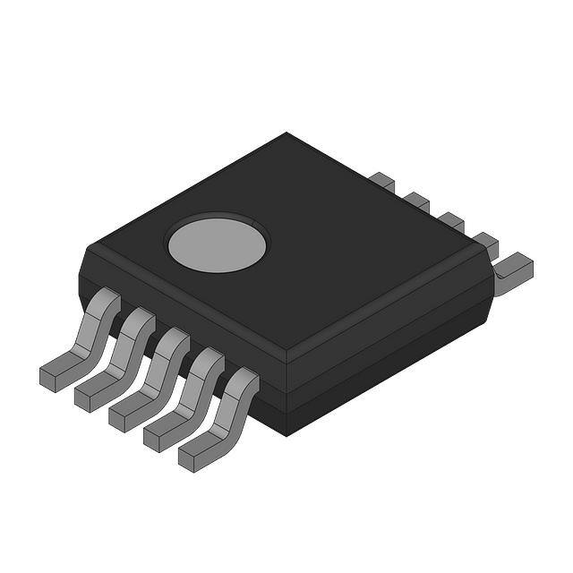
10-Lead VSSOP Package
Internal Push-Pull Driver With 1-A Peak Current
Capability
Current Limit and Thermal Shutdown
Frequency Compensation Optimized With a
Capacitor and a Resistor
Internal Softstart
Current Mode Operation
Adjustable Undervoltage Lockout With Hysteresis
Pulse Skipping at Light Loads
Key Specifications
– Wide Supply Voltage Range of 2.97 V to 48 V
– 100-kHz to 1-MHz Adjustable and
Synchronizable Clock Frequency
– ±1.5% (Over Temperature) Internal Reference
– 10-µA Shutdown Current (Over Temperature)
Create a Custom Design Using the LM3481 with
the WEBENCH Power Designer
The LM3481 device has built-in protection features
such as thermal shutdown, short-circuit protection
and overvoltage protection. Power-saving shutdown
mode reduces the total supply current to 5 µA and
allows power supply sequencing. Internal soft-start
limits the inrush current at start-up. Integrated current
slope compensation simplifies the design and, if
needed for specific applications, can be increased
using a single resistor.
Device Information(1)
PART NUMBER
2 Applications
LM3481
•
•
•
LM3481-Q1
•
•
•
•
Automotive Start-Stop Applications
Automotive ADAS Driver Information
One Cell/Two Cell Li-ion Battery Powered
Portable Bluetooth Audio Systems
Notebooks, PDAs, Digital Cameras, and Other
Portable Applications
Offline Power Supplies
Set-Top Boxes
Boost for Audio Amplifiers
PACKAGE
VSSOP (10)
VIN = 5V
R8
121 k:
ISEN
VIN
UVLO
L1
6.8 PH
1 PF
VCC
C9
COMP
RC
22.6 k:
CC
82 nF
FB
RF2
20 k:
RF1
169 k:
AGND
3.00 mm × 3.00 mm
(1) For all available packages, see the orderable addendum at
the end of the data sheet.
R7
121 k:
C8
390 pF
BODY SIZE (NOM)
LM3481
Q1
DR
D1
+ CIN1, CIN2
150 PF
VOUT = 12V
IOUT = 1.8A
+ COUT1, COUT2
150 PF
PGND
FA/SYNC/SD
RFA
90.9 k:
CSEN
1 nF
RSEN
20 m:
Figure 1. LM3481 Typical 5V to 12V Boost Converter Application
1
An IMPORTANT NOTICE at the end of this data sheet addresses availability, warranty, changes, use in safety-critical applications,
intellectual property matters and other important disclaimers. PRODUCTION DATA.
�LM3481, LM3481-Q1
SNVS346F – NOVEMBER 2007 – REVISED NOVEMBER 2014
www.ti.com
Table of Contents
1
2
3
4
5
6
7
Features ..................................................................
Applications ...........................................................
Description .............................................................
Revision History.....................................................
Pin Configuration and Functions .........................
Specifications.........................................................
1
1
1
2
3
4
6.1
6.2
6.3
6.4
6.5
6.6
6.7
4
4
4
4
5
5
8
Absolute Maximum Ratings ......................................
Handling Ratings: LM3481........................................
Handling Ratings: LM3481-Q1..................................
Recommended Operating Ratings............................
Thermal Information ..................................................
Electrical Characteristics...........................................
Typical Characteristics ..............................................
Detailed Description ............................................ 11
7.1 Overview ................................................................. 11
7.2 Functional Block Diagram ....................................... 12
7.3 Feature Description................................................. 12
7.4 Device Functional Modes........................................ 18
8
Application and Implementation ........................ 19
8.1 Application Information............................................ 19
8.2 Typical Applications ................................................ 19
9 Power Supply Recommendations...................... 30
10 Layout................................................................... 30
10.1 Layout Guidelines ................................................. 30
10.2 Layout Example .................................................... 31
11 Device and Documentation Support ................. 32
11.1
11.2
11.3
11.4
11.5
Documentation Support ........................................
Related Links ........................................................
Trademarks ...........................................................
Electrostatic Discharge Caution ............................
Glossary ................................................................
32
32
32
32
32
12 Mechanical, Packaging, and Orderable
Information ........................................................... 33
4 Revision History
Changes from Revision E (April 2012) to Revision F
•
2
Page
Added Pin Configuration and Functions section, Handling Rating table, Feature Description section, Device
Functional Modes, Application and Implementation section, Power Supply Recommendations section, Layout
section, Device and Documentation Support section, and Mechanical, Packaging, and Orderable Information
section ................................................................................................................................................................................... 1
Submit Documentation Feedback
Copyright © 2007–2014, Texas Instruments Incorporated
Product Folder Links: LM3481 LM3481-Q1
�LM3481, LM3481-Q1
www.ti.com
SNVS346F – NOVEMBER 2007 – REVISED NOVEMBER 2014
5 Pin Configuration and Functions
10-Pin
VSSOP Package
Top View
ISEN
UVLO
COMP
FB
AGND
1
10
2
9
3
8
LM3481
4
7
5
6
VIN
VCC
DR
PGND
FA/SYNC/SD
Pin Functions
PIN
I/O
DESCRIPTION
NO.
NAME
1
ISEN
A
Current sense input pin. Voltage generated across an external sense resistor is fed into this pin.
2
UVLO
A
Under voltage lockout pin. A resistor divider from VIN to ground is connected to the UVLO pin. The
ratio of these resistances determine the input voltage which allows switching and the hysteresis to
disable switching.
3
COMP
A
Compensation pin. A resistor and capacitor combination connected to this pin provides
compensation for the control loop.
4
FB
A
Feedback pin. Inverting input of the error amplifier.
5
AGND
G
Analog ground pin. Internal bias circuitry reference. Should be connected to PGND at a single
point.
6
FA/SYNC/SD
I/A
7
PGND
G
Power ground pin. External power circuitry reference. Should be connected to AGND at a single
point.
8
DR
O
Drive pin of the IC. The gate of the external MOSFET should be connected to this pin.
9
VCC
O
Driver supply voltage pin. A bypass capacitor must be connected from this pin to PGND. See
Driver Supply Capacitor Selection section. Do not bias externally.
10
VIN
P
Power supply input pin.
Frequency adjust, synchronization, and shutdown pin. A resistor connected from this pin to ground
sets the oscillator frequency. An external clock signal at this pin will synchronize the controller to
the frequency of the clock. A high level on this pin for ≥ 30 µs will turn the device off and the device
will then draw 5 µA from the supply typically.
Copyright © 2007–2014, Texas Instruments Incorporated
Product Folder Links: LM3481 LM3481-Q1
Submit Documentation Feedback
3
�LM3481, LM3481-Q1
SNVS346F – NOVEMBER 2007 – REVISED NOVEMBER 2014
www.ti.com
6 Specifications
6.1 Absolute Maximum Ratings
over operating free-air temperature range (unless otherwise noted) (1)
MIN
MAX
UNIT
VIN
Pin Voltage
–0.4
50
V
FB
Pin Voltage
–0.4
6
V
FA/SYNC/SD
Pin Voltage
–0.4
6
V
COMP
Pin Voltage
–0.4
6
V
UVLO
Pin Voltage
–0.4
6
V
VCC
Pin Voltage
–0.4
6.5
V
DR
Pin Voltage
–0.4
6
V
ISEN
Pin Voltage
–400
600
mV
1
A
Peak Driver Output Current
Power Dissipation
Lead Temperature
(only applies to
operating conditions)
Peak Body
Temperature
(1)
(2)
Internally Limited
Junction Temperature
150
°C
DGS Package
220
°C
260
°C
(2)
Absolute Maximum Ratings are limits beyond which damage to the device may occur. Recommended Operating Ratings indicates
conditions for which the device is intended to be functional, but does not ensure specific performance limits. For ensured specifications
and test conditions, see the Electrical Characteristics. The ensured specifications apply only for the test conditions.
Part is MSL1-260C qualified
6.2 Handling Ratings: LM3481
Tstg
V(ESD)
(1)
(2)
MIN
MAX
UNIT
–65
150
°C
Human body model (HBM), per ANSI/ESDA/JEDEC JS-001, all
pins (1)
–2000
+2000
Charged device model (CDM), per JEDEC specification
JESD22-C101, all pins (2)
–750
+750
Storage temperature range
Electrostatic discharge
V
JEDEC document JEP155 states that 500-V HBM allows safe manufacturing with a standard ESD control process.
JEDEC document JEP157 states that 250-V CDM allows safe manufacturing with a standard ESD control process.
6.3 Handling Ratings: LM3481-Q1
Tstg
MIN
MAX
UNIT
–65
150
°C
–2000
+2000
Corner pins (1, 5, 6,
and 10)
–750
+750
Other pins
–750
+750
Storage temperature range
Human body model (HBM), per AEC Q100-002 (1)
V(ESD)
(1)
Electrostatic discharge
Charged device model (CDM), per
AEC Q100-011
V
AEC Q100-002 indicates HBM stressing is done in accordance with the ANSI/ESDA/JEDEC JS-001 specification.
6.4 Recommended Operating Ratings
MIN
MAX
UNIT
Supply Voltage
2.97
48
V
Junction Temperature Range
–40
125
°C
Switching Frequency Range
100
1
4
Submit Documentation Feedback
kHz/MHz
Copyright © 2007–2014, Texas Instruments Incorporated
Product Folder Links: LM3481 LM3481-Q1
�LM3481, LM3481-Q1
www.ti.com
SNVS346F – NOVEMBER 2007 – REVISED NOVEMBER 2014
6.5 Thermal Information
LM3481
THERMAL METRIC (1)
VSSOP
UNIT
10 PINS
RθJA
Junction-to-ambient thermal resistance
157.3
RθJC(top)
Junction-to-case (top) thermal resistance
51.1
RθJB
Junction-to-board thermal resistance
76.9
ψJT
Junction-to-top characterization parameter
5.0
ψJB
Junction-to-board characterization parameter
75.6
RθJC(bot)
Junction-to-case (bottom) thermal resistance
-
(1)
°C/W
For more information about traditional and new thermal metrics, see the IC Package Thermal Metrics application report, SPRA953.
6.6 Electrical Characteristics
VIN= 12 V, RFA= 40 kΩ, TJ = 25°C, unless otherwise indicated.
PARAMETER
TEST CONDITIONS
MIN
VCOMP = 1.4 V, 2.97 ≤ VIN ≤ 48 V
TYP
MAX
UNIT
1.275
VFB
Feedback Voltage
VCOMP = 1.4 V, 2.97 ≤ VIN ≤ 48 V,
–40°C ≤ TJ ≤ 125°C
ΔVLINE
Feedback Voltage Line Regulation
2.97 ≤ VIN ≤ 48 V
0.003
%/V
ΔVLOAD
Output Voltage Load Regulation
IEAO Source/Sink
±0.5
%/A
VUVLOSEN
Undervoltage Lockout Reference
Voltage
IUVLO
UVLO Source Current
VUVLOSD
UVLO Shutdown Voltage
ICOMP
COMP pin Current Sink
1.256
VUVLO Ramping Down
VUVLO Ramping Down, –40°C ≤ TJ ≤
125°C
1.345
1.517
5
3
0.55
VFB = 0V
VCOMP
V
1.430
Enabled
Enabled, –40°C ≤ TJ ≤ 125°C
1.294
VFB = 1.275V
RFA = 40 kΩ
6
0.7
0.82
V
µA
V
640
µA
1
V
475
fnom
Nominal Switching Frequency
Vsync-HI
Threshold for Synchronization on
FA/SYNC/SD pin
Synchronization Voltage Rising
1.4
V
Vsync-LOW
Threshold for Synchronization on
FA/SYNC/SD pin
Synchronization Voltage Falling
0.7
V
RDS1 (ON)
Driver Switch On Resistance (top)
IDR = 0.2A, VIN= 5 V
4
Ω
RDS2 (ON)
Driver Switch On Resistance (bottom)
IDR = 0.2A
2
Ω
RFA = 40 kΩ, –40°C ≤ TJ ≤ 125°C
VDR (max)
Maximum Drive Voltage Swing (1)
Dmax
Maximum Duty Cycle
tmin (on)
Minimum On Time
ISUPPLY
(1)
(2)
406
550
VIN < 6V
VIN
VIN ≥ 6V
6
RFA=40 kΩ
81%
250
See
Supply Current (switching)
See (2), –40°C ≤ TJ ≤ 125°C
V
85%
worst case over temperature
(2)
kHz
363
ns
571
ns
3.7
5.0
mA
The drive pin voltage, VDR, is equal to the input voltage when input voltage is less than 6 V. VDR is equal to 6 V when the input voltage
is greater than or equal to 6 V.
For this test, the FA/SYNC/SD Pin is pulled to ground using a 40-kΩ resistor.
Copyright © 2007–2014, Texas Instruments Incorporated
Product Folder Links: LM3481 LM3481-Q1
Submit Documentation Feedback
5
�LM3481, LM3481-Q1
SNVS346F – NOVEMBER 2007 – REVISED NOVEMBER 2014
www.ti.com
Electrical Characteristics (continued)
VIN= 12 V, RFA= 40 kΩ, TJ = 25°C, unless otherwise indicated.
PARAMETER
TEST CONDITIONS
VFA/SYNC/SD = 3 V
IQ
Quiescent Current in Shutdown Mode
MIN
(3)
, VIN = 12 V
TYP
15
VFA/SYNC/SD = 3 V (3), VIN = 5 V
Current Sense Threshold Voltage
VSC
Over Load Current Limit Sense Voltage
VSL
Internal Compensation Ramp Voltage
VOVP
Output Over-voltage Protection (with
respect to feedback voltage) (4)
VCOMP = 1.4 V
VOVP(HYS)
Output Over-Voltage Protection
Hysteresis
VCOMP = 1.4 V
10
Gm
Error Amplifier Transconductance
–40°C ≤ TJ ≤ 125°C
100
–40°C ≤ TJ ≤ 125°C
157
VCOMP = 1.4 V, –40°C ≤ TJ ≤ 125°C
26
70
VCOMP = 1.4 V
216
mV
690
mV
mV
µmho
60
VCOMP = 1.4 V, IEAO = 100 µA
(Source/Sink), –40°C ≤ TJ ≤ 125°C
V/V
35
Source, VCOMP = 1.4 V, VFB = 1.1 V,
–40°C ≤ TJ ≤ 125°C
66
640
475
Sink, VCOMP = 1.4 V, VFB = 1.4 V
837
µA
65
31
Upper Limit: VFB = 0 V, COMP Pin
Floating
Error Amplifier Output Voltage Swing
106
450
VCOMP = 1.4 V, –40°C ≤ TJ ≤ 125°C
Sink, VCOMP = 1.4 V, VFB = 1.4 V,
–40°C ≤ TJ ≤ 125°C
VEAO
135
28
mV
mV
85
VCOMP = 1.4 V, IEAO = 100 µA
(Source/Sink)
Error Amplifier Output Current (Source/
Sink)
275
90
Source, VCOMP = 1.4 V, VFB = 1.1 V
IEAO
190
220
VCOMP = 1.4 V, –40°C ≤ TJ ≤ 125°C
Error Amplifier Voltage Gain
µA
5
160
VSENSE
UNIT
9
VFA/SYNC/SD = 3 V (3), VIN = 12 V,
–40°C ≤ TJ ≤ 125°C
VFA/SYNC/SD = 3 V (3), VIN = 5 V, –40°C
≤ TJ ≤ 125°C
AVOL
MAX
Upper Limit: VFB = 0 V, COMP Pin
Floating, –40°C ≤ TJ ≤ 125°C
100
µA
2.70
V
2.45
Lower Limit: VFB = 1.4 V
2.93
0.60
Lower Limit: VFB = 1.4 V, –40°C ≤ TJ
≤ 125°C
0.32
8.7
0.90
tSS
Internal Soft-Start Delay
VFB = 1.2 V, COMP Pin Floating
tr
Drive Pin Rise Time
Cgs = 3000 pf, VDR = 0 V to 3 V
25
ns
tf
Drive Pin Fall Time
Cgs = 3000 pf, VDR = 3 V to 0 V
25
ns
Output = High (Shutdown)
VSD
Shutdown signal
threshold (5)FA/SYNC/SD pin
(5)
6
21.3
ms
1.31
Output = High (Shutdown), –40°C ≤
TJ ≤ 125°C
1.40
Output = Low (Enable)
V
0.68
Output = Low (Enable), –40°C ≤ TJ ≤
125°C
(3)
(4)
15
V
0.40
V
For this test, the FA/SYNC/SD Pin is pulled to 3 V using a 40-kΩ resistor.
The overvoltage protection is specified with respect to the feedback voltage. This is because the overvoltage protection tracks the
feedback voltage. The overvoltage threshold can be calculated by adding the feedback voltage (VFB) to the overvoltage protection
specification.
The FA/SYNC/SD pin should be pulled to VIN through a resistor to turn the regulator off. The voltage on the FA/SYNC/SD pin must be
above the max limit for the Output = High longer than 30 µs to keep the regulator off and must be below the minimum limit for Output =
Low to keep the regulator on.
Submit Documentation Feedback
Copyright © 2007–2014, Texas Instruments Incorporated
Product Folder Links: LM3481 LM3481-Q1
�LM3481, LM3481-Q1
www.ti.com
SNVS346F – NOVEMBER 2007 – REVISED NOVEMBER 2014
Electrical Characteristics (continued)
VIN= 12 V, RFA= 40 kΩ, TJ = 25°C, unless otherwise indicated.
PARAMETER
TEST CONDITIONS
ISD
Shutdown Pin Current FA/SYNC/SD
pin
TSD
Thermal Shutdown
Tsh
Thermal Shutdown Hysteresis
MIN
TYP
VSD = 5 V
−1
VSD = 0 V
20
Copyright © 2007–2014, Texas Instruments Incorporated
Product Folder Links: LM3481 LM3481-Q1
MAX
UNIT
µA
165
°C
10
°C
Submit Documentation Feedback
7
�LM3481, LM3481-Q1
SNVS346F – NOVEMBER 2007 – REVISED NOVEMBER 2014
www.ti.com
6.7 Typical Characteristics
Unless otherwise specified, VIN = 12 V, TJ = 25°C.
8
Figure 3. Comp Pin Voltage vs. Load Current
Figure 4. Switching Frequency vs. RFA
Figure 5. Efficiency vs. Load Current (3.3 VIN and 12 VOUT)
Figure 6. Efficiency vs. Load Current (5 VIN and 12 VOUT)
Figure 7. Efficiency vs. Load Current (9 VIN and 12 VOUT)
Figure 8. Frequency vs. Temperature
Submit Documentation Feedback
Copyright © 2007–2014, Texas Instruments Incorporated
Product Folder Links: LM3481 LM3481-Q1
�LM3481, LM3481-Q1
www.ti.com
SNVS346F – NOVEMBER 2007 – REVISED NOVEMBER 2014
Typical Characteristics (continued)
Unless otherwise specified, VIN = 12 V, TJ = 25°C.
Figure 9. COMP Pin Source Current vs. Temperature
Figure 10. ISupplyvs. Input Voltage (Nonswitching)
Figure 11. ISupply vs. Input Voltage (Switching)
Figure 12. Shutdown Threshold Hysteresis vs. Temperature
Figure 13. Drive Voltage vs. Input Voltage
Figure 14. Short Circuit Protection vs. VIN
Copyright © 2007–2014, Texas Instruments Incorporated
Product Folder Links: LM3481 LM3481-Q1
Submit Documentation Feedback
9
�LM3481, LM3481-Q1
SNVS346F – NOVEMBER 2007 – REVISED NOVEMBER 2014
www.ti.com
Typical Characteristics (continued)
Unless otherwise specified, VIN = 12 V, TJ = 25°C.
Figure 15. Current Sense Threshold vs. Input Voltage
Figure 16. Compensation Ramp Amplitude vs. Input Voltage
Figure 17. Minimum On-Time vs. Temperature
10
Submit Documentation Feedback
Copyright © 2007–2014, Texas Instruments Incorporated
Product Folder Links: LM3481 LM3481-Q1
�LM3481, LM3481-Q1
www.ti.com
SNVS346F – NOVEMBER 2007 – REVISED NOVEMBER 2014
7 Detailed Description
7.1 Overview
The LM3481 device uses a fixed frequency, Pulse Width Modulated (PWM), current mode control architecture. In
a typical application circuit, the peak current through the external MOSFET is sensed through an external sense
resistor. The voltage across this resistor is fed into the ISEN pin. This voltage is then level shifted and fed into the
positive input of the PWM comparator. The output voltage is also sensed through an external feedback resistor
divider network and fed into the error amplifier (EA) negative input (feedback pin, FB). The output of the error
amplifier (COMP pin) is added to the slope compensation ramp and fed into the negative input of the PWM
comparator.
At the start of any switching cycle, the oscillator sets the RS latch using the SET/Blank-out and switch logic
blocks. This forces a high signal on the DR pin (gate of the external MOSFET) and the external MOSFET turns
on. When the voltage on the positive input of the PWM comparator exceeds the negative input, the RS latch is
reset and the external MOSFET turns off.
The voltage sensed across the sense resistor generally contains spurious noise spikes, as shown in Figure 18.
These spikes can force the PWM comparator to reset the RS latch prematurely. To prevent these spikes from
resetting the latch, a blank-out circuit inside the IC prevents the PWM comparator from resetting the latch for a
short duration after the latch is set. This duration, called the blank-out time, is typically 250 ns and is specified as
tmin (on) in the Electrical Characteristics section.
Under extremely light load or no-load conditions, the energy delivered to the output capacitor when the external
MOSFET is on during the blank-out time is more than what is delivered to the load. An overvoltage comparator
inside the LM3481 prevents the output voltage from rising under these conditions by sensing the feedback (FB
pin) voltage and resetting the RS latch. The latch remains in a reset state until the output decays to the nominal
value. Thus the operating frequency decreases at light loads, resulting in excellent efficiency.
Blank-Out prevents false
reset
PWM Comparator resets
the RS latch
VSL
_
+
PWM
Comparator
Oscillator Sets
the RS Latch
Tmin (on) Blank-Out time
Figure 18. Basic Operation of the PWM Comparator
Copyright © 2007–2014, Texas Instruments Incorporated
Product Folder Links: LM3481 LM3481-Q1
Submit Documentation Feedback
11
�LM3481, LM3481-Q1
SNVS346F – NOVEMBER 2007 – REVISED NOVEMBER 2014
www.ti.com
7.2 Functional Block Diagram
Shutdown Detect
VIN
SYNC/Fixed
Frequency detect
FA/SYNC/SD
Oscillator
Set/Blankout
Slope
Compensation
6V
Soft-start
UVLO
Bias
Voltages
UVLO
Thermal
Shutdown
40 éA
1.275V
Reference
Ramp
Adjust
-
COMP
+
6
V-I
Converter
EA
Vfb + Vovp
Overvoltage
Comparator
Switch
Logic
+
+
FB
I-V
Converter
PWM
Comparator
R
-
S
Q
+
VCC
220 mV
ISEN
Short-circuit
Comparator
One Shot
+
Switch
Driver
DR
Level Shifter
AGND
PGND
Figure 19. LM3481 Simplified Functional Block Diagram
7.3 Feature Description
7.3.1 Overvoltage Protection
The LM3481 has overvoltage protection (OVP) for the output voltage. OVP is sensed at the feedback pin (FB). If
at anytime the voltage at the feedback pin rises to VFB + VOVP, OVP is triggered. See the Electrical
Characteristics section for limits on VFB and VOVP.
OVP will cause the drive pin (DR) to go low, forcing the power MOSFET off. With the MOSFET off, the output
voltage will drop. The LM3481 will begin switching again when the feedback voltage reaches VFB + (VOVP VOVP(HYS)). See the Electrical Characteristics section for limits on VOVP(HYS). The Error Amplifier is operationnal
during OVP events.
7.3.2 Bias Voltage
The internal bias of the LM3481 comes from either the internal bias voltage generator as shown in the block
diagram or directly from the voltage at the VIN pin. At input voltages lower than 6 V the internal IC bias is the
input voltage and at voltages above 6 V the internal bias voltage generator of the LM3481 provides the bias. The
voltage for the gate driver is output on the VCC pin for compensation by an external capacitor (0.47µF to 4.7µF
depending on the FET requirements). Biasing the VCC pin by an external voltage source should not be
attempted.
12
Submit Documentation Feedback
Copyright © 2007–2014, Texas Instruments Incorporated
Product Folder Links: LM3481 LM3481-Q1
�LM3481, LM3481-Q1
www.ti.com
SNVS346F – NOVEMBER 2007 – REVISED NOVEMBER 2014
Feature Description (continued)
7.3.3 Slope Compensation Ramp
The LM3481 uses a current mode control scheme. The main advantages of current mode control are inherent
cycle-by-cycle current limit for the switch and simpler control loop characteristics. It is easy to parallel power
stages using current mode control because current sharing is automatic. However there is a natural instability
that will occur for duty cycles, D, greater than 50% if additional slope compensation is not addressed as
described below.
The current mode control scheme samples the inductor current, IL, and compares the sampled signal, Vsamp, to a
internally generated control signal, Vc. The current sense resistor, RSEN, as shown in Figure 23, converts the
sampled inductor current, IL, to the voltage signal, Vsamp, that is proportional to IL such that:
Vsamp = IL x RSEN
(1)
The rising and falling slopes, M1 and −M2 respectively, of Vsamp are also proportional to the inductor current rising
and falling slopes, Mon and −Moff respectively. Where Mon is the inductor slope during the switch on-time and
−Moff is the inductor slope during the switch off-time and are related to M1 and −M2 by:
M1 = Mon x RSEN
−M2 = −Moff x RSEN
(2)
(3)
For the boost topology:
Mon = VIN / L
−Moff = (VIN − VOUT) / L
M1 = [VIN / L] x RSEN
−M2 = [(VIN − VOUT) / L] x RSEN
M2 = [(VOUT − VIN) / L] x RSEN
(4)
(5)
(6)
(7)
(8)
Current mode control has an inherent instability for duty cycles greater than 50%, as shown in Figure 20, where
the control signal slope, MC, equals zero. In Figure 20, a small increase in the load current causes the sampled
signal to increase by ΔVsamp0. The effect of this load change, ΔVsamp1, at the end of the first switching cycle is :
'Vsamp1 = -
M2
D
'Vsamp0
'Vsamp0 = M1
1-D
(9)
From Equation 9, when D > 0.5, ΔVsamp1 will be greater than ΔVsamp0. In other words, the disturbance is
divergent. So a very small perturbation in the load will cause the disturbance to increase. To ensure that the
perturbed signal converges we must maintain:
-
M2 <
M1 1
(10)
Control Signal MC = 0
Perturbed Signal
'Vsamp0
-M2
_
M1
'Vsamp1
Steady State
Signal Vsamp
+
PWM
Comparator
(1-D)TS
DTS
Figure 20. Subharmonic Oscillation for D>0.5
Copyright © 2007–2014, Texas Instruments Incorporated
Product Folder Links: LM3481 LM3481-Q1
Submit Documentation Feedback
13
�LM3481, LM3481-Q1
SNVS346F – NOVEMBER 2007 – REVISED NOVEMBER 2014
www.ti.com
Feature Description (continued)
Control Signal
Compensation Ramp
-MC
VSL
Perturbed Signal
-M2
M1
'Vsamp0
_
Vsamp
+
PWM
Comparator
'Vsamp1
Steady State
Signal Vsamp
DTS
Control
Signal
(1-D)TS
Figure 21. Compensation Ramp Avoids Subharmonic Oscillation
To prevent the subharmonic oscillations, a compensation ramp is added to the control signal, as shown in
Figure 21.
With the compensation ramp, ΔVsamp1 and the convergence criteria are expressed by,
'Vsamp1 = -
-
M2 - MC
'Vsamp0
M 1 + MC
(11)
M 2 - MC
ΔiL
(22)
(23)
(24)
Choose the minimum IOUT to determine the minimum L. A common choice is to set (2 x ΔiL) to 30% of IL.
Choosing an appropriate core size for the inductor involves calculating the average and peak currents expected
through the inductor. In a boost converter,
IL =
IOUT
1-D
(25)
(26)
IL_peak = IL(max) + ΔiL(max)
'iL =
DVIN
2LfS
(27)
Copyright © 2007–2014, Texas Instruments Incorporated
Product Folder Links: LM3481 LM3481-Q1
Submit Documentation Feedback
21
�LM3481, LM3481-Q1
SNVS346F – NOVEMBER 2007 – REVISED NOVEMBER 2014
www.ti.com
Typical Applications (continued)
A core size with ratings higher than these values should be chosen. If the core is not properly rated, saturation
will dramatically reduce overall efficiency.
The LM3481 can be set to switch at very high frequencies. When the switching frequency is high, the converter
can operate with very small inductor values. With a small inductor value, the peak inductor current can be
extremely higher than the output currents, especially under light load conditions.
The LM3481 senses the peak current through the switch. The peak current through the switch is the same as the
peak current calculated above.
8.2.1.2.3 Programming the Output Voltage and Output Current
The output voltage can be programmed using a resistor divider between the output and the feedback pins, as
shown in Figure 33. The resistors are selected such that the voltage at the feedback pin is 1.275 V. RF1 and RF2
can be selected using the equation,
VOUT = 1.275 (1+
RF1
)
RF2
(28)
A 100-pF capacitor may be connected between the feedback and ground pins to reduce noise.
The maximum amount of current that can be delivered at the output can be controlled by the sense resistor,
RSEN. Current limit occurs when the voltage that is generated across the sense resistor equals the current sense
threshold voltage, VSENSE. Limits for VSENSE have been specified in the Electrical Characteristics section. This can
be expressed as:
Isw(peak) x RSEN = VSENSE- D x VSL
(29)
The peak current through the switch is equal to the peak inductor current.
Isw(peak) = IL(max) + ΔiL
(30)
Therefore for a boost converter,
Isw(peak) =
(D x VIN)
IOUT(max)
+
(1-D)
(2 x fS x L)
(31)
Combining the two equations yields an expression for RSEN,
RSEN =
VSENSE - (D x VSL)
IOUT(max)
(1-D)
+
(D x VIN)
(2 x fS x L)
(32)
Evaluate RSEN at the maximum and minimum VIN values and choose the smallest RSEN calculated.
VIN
L
D1
DR
VOUT
Q
+
LM3481
COUT
ISEN
FB
RF1
RSEN
RF2
Figure 33. Adjusting the Output Voltage
22
Submit Documentation Feedback
Copyright © 2007–2014, Texas Instruments Incorporated
Product Folder Links: LM3481 LM3481-Q1
�LM3481, LM3481-Q1
www.ti.com
SNVS346F – NOVEMBER 2007 – REVISED NOVEMBER 2014
Typical Applications (continued)
8.2.1.2.4 Current Limit With Additional Slope Compensation
If an external slope compensation resistor is used (see Figure 23) the internal control signal will be modified and
this will have an effect on the current limit.
If RSL is used, then this will add to the existing slope compensation. The command voltage, VCS, will then be
given by:
VCS = VSENSE − D x (VSL + ΔVSL)
(33)
Where VSENSE is a defined parameter in the Electrical Characteristics section and ΔVSL is the additional slope
compensation generated as discussed in the Slope Compensation Ramp section. This changes the equation for
RSEN to:
RSEN =
VSENSE - D x (VSL+'VSL)
IOUT(max)
(1-D)
+
(D x VIN)
(2 x fS x L)
(34)
Note that because ΔVSL = RSL x K as defined earlier, RSLcan be used to provide an additional method for setting
the current limit. In some designs RSL can also be used to help filter noise to keep the ISEN pin quiet.
8.2.1.2.5 Power Diode Selection
Observation of the boost converter circuit shows that the average current through the diode is the average load
current, and the peak current through the diode is the peak current through the inductor. The diode should be
rated to handle more than the inductor peak current. The peak diode current can be calculated using the formula:
ID(Peak) = [IOUT/ (1−D)] + ΔiL
(35)
In Equation 35, IOUT is the output current and ΔiL has been defined in Figure 32.
The peak reverse voltage for a boost converter is equal to the regulator output voltage. The diode must be
capable of handling this peak reverse voltage. To improve efficiency, a low forward drop Schottky diode is
recommended.
8.2.1.2.6 Power MOSFET Selection
The drive pin, DR, of the LM3481 must be connected to the gate of an external MOSFET. In a boost topology,
the drain of the external N-Channel MOSFET is connected to the inductor and the source is connected to the
ground. The drive pin voltage, VDR, depends on the input voltage (see Typical Characteristics). In most
applications, a logic level MOSFET can be used. For very low input voltages, a sub-logic level MOSFET should
be used.
The selected MOSFET directly controls the efficiency. The critical parameters for selection of a MOSFET are:
• Minimum threshold voltage, VTH(MIN)
• On-resistance, RDS(ON)
• Total gate charge, Qg
• Reverse transfer capacitance, CRSS
• Maximum drain to source voltage, VDS(MAX)
The off-state voltage of the MOSFET is approximately equal to the output voltage. VDS(MAX) of the MOSFET must
be greater than the output voltage. The power losses in the MOSFET can be categorized into conduction losses
and ac switching or transition losses. RDS(ON) is needed to estimate the conduction losses. The conduction loss,
PCOND, is the I2R loss across the MOSFET. The maximum conduction loss is given by:
PCOND(MAX) =
IOUT(max) 2
DMAXRDS(ON)
1 - DMAX
(36)
where DMAX is the maximum duty cycle.
DMAX = 1-
VIN(MIN)
VOUT
(37)
At high switching frequencies the switching losses may be the largest portion of the total losses.
Copyright © 2007–2014, Texas Instruments Incorporated
Product Folder Links: LM3481 LM3481-Q1
Submit Documentation Feedback
23
�LM3481, LM3481-Q1
SNVS346F – NOVEMBER 2007 – REVISED NOVEMBER 2014
www.ti.com
Typical Applications (continued)
The switching losses are very difficult to calculate due to changing parasitics of a given MOSFET in operation.
Often, the individual MOSFET datasheet does not give enough information to yield a useful result. Equation 38
and Equation 39 give a rough idea how the switching losses are calculated:
ILmax x Vout
x fSW x (tLH + tHL)
2
RGate
Qgs
x
tLH = Qgd +
VDR - Vgsth
2
PSW =
(38)
(39)
8.2.1.2.7 Input Capacitor Selection
Due to the presence of an inductor at the input of a boost converter, the input current waveform is continuous
and triangular, as shown in Figure 32. The inductor ensures that the input capacitor sees fairly low ripple
currents. However, as the input capacitor gets smaller, the input ripple goes up. The rms current in the input
capacitor is given by:
ICIN(RMS) = 'iL / 3 =
(VOUT - VIN)VIN
12 VOUTLfS
(40)
The input capacitor should be capable of handling the rms current. Although the input capacitor is not as critical
in a boost application, low values can cause impedance interactions. Therefore a good quality capacitor should
be chosen in the range of 100 µF to 200 µF. If a value lower than 100 µF is used, then problems with impedance
interactions or switching noise can affect the LM3481. To improve performance, especially with VIN below 8 V, it
is recommended to use a 20Ω resistor at the input to provide a RC filter. This resistor is placed in series with the
VIN pin with only a bypass capacitor attached to the VIN pin directly (see Figure 34). A 0.1-µF or 1-µF ceramic
capacitor is necessary in this configuration. The bulk input capacitor and inductor will connect on the other side
of the resistor with the input power supply.
RIN
VIN
VIN
LM3481
CBYPASS
CIN
Figure 34. Reducing IC Input Noise
8.2.1.2.8 Output Capacitor Selection
The output capacitor in a boost converter provides all the output current when the inductor is charging. As a
result it sees very large ripple currents. The output capacitor should be capable of handling the maximum rms
current. The rms current in the output capacitor is:
(41)
Where
'iL =
DVIN
2LfS
(42)
and D, the duty cycle is equal to (VOUT − VIN)/VOUT.
The ESR and ESL of the output capacitor directly control the output ripple. Use capacitors with low ESR and ESL
at the output for high efficiency and low ripple voltage. Surface mount tantalums, surface mount polymer
electrolytic and polymer tantalum, Sanyo- OSCON, or multi-layer ceramic capacitors are recommended at the
output.
8.2.1.2.9
Driver Supply Capacitor Selection
A good quality ceramic bypass capacitor must be connected from the VCC pin to the PGND pin for proper
operation. This capacitor supplies the transient current required by the internal MOSFET driver, as well as
filtering the internal supply voltage for the controller. A value of between 0.47 µF and 4.7 µF is recommended.
24
Submit Documentation Feedback
Copyright © 2007–2014, Texas Instruments Incorporated
Product Folder Links: LM3481 LM3481-Q1
�LM3481, LM3481-Q1
www.ti.com
SNVS346F – NOVEMBER 2007 – REVISED NOVEMBER 2014
Typical Applications (continued)
8.2.1.2.10 Compensation
For detailed explanation on how to select the right compensation components to attach to the compensation pin
for a boost topology please see AN-1286 Compensation for the LM3478 Boost Controller (SNVA067). When
calculating the Error Amplifier DC gain, AEA, ROUT = 152 kΩ for the LM3481.
8.2.1.3 Application Curve
Figure 35. Start-Up Pattern for a 5-Vin, 12-Vout Boost Converter Using LM3481 Boost Evaluation Module
(C1: Inductor Current, C2: Vin, C3:Vout)
Copyright © 2007–2014, Texas Instruments Incorporated
Product Folder Links: LM3481 LM3481-Q1
Submit Documentation Feedback
25
�LM3481, LM3481-Q1
SNVS346F – NOVEMBER 2007 – REVISED NOVEMBER 2014
www.ti.com
Typical Applications (continued)
8.2.2 Typical SEPIC Converter
R7
10 k:
VIN = 3.0V to 24V
D2
5.1V
VIN
ISEN
0.47 µF
RC
4.7 k:
CC
0.1 PF
UVLO
COMP
FB
RF2
20 k:
+ CIN
15 PF, 35V x2
L1
10 PH
1 PF, ceramic
LM3481
CS
Q1
IRF7807
DR
PGND
AGND
MBRS130LT3
VCC
D1
L2
10 PH
VOUT = 5V, 1A
+ COUT
100 PF, 10V
FA/SYNC/SD
RFA
40 k:
RF1
60 k:
CSEN
1 nF
RSEN
0.05:
Figure 36. Typical SEPIC Converter using LM3481
Because the LM3481 controls a low-side N-Channel MOSFET, it can also be used in SEPIC (Single Ended
Primary Inductance Converter) applications. An example of SEPIC using the LM3481 is shown in Figure 36. As
shown in Figure 36, the output voltage can be higher or lower than the input voltage. The SEPIC uses two
inductors to step-up or step-down the input voltage. The inductors L1 and L2 can be two discrete inductors or
two windings of a coupled transformer because equal voltages are applied across the inductor throughout the
switching cycle. Using two discrete inductors allows use of catalog magnetics, as opposed to a custom
transformer. The input ripple can be reduced along with size by using the coupled windings of transformer for L1
and L2.
Due to the presence of the inductor L1 at the input, the SEPIC inherits all the benefits of a boost converter. One
main advantage of SEPIC over a boost converter is the inherent input to output isolation. The capacitor CS
isolates the input from the output and provides protection against shorted or malfunctioning load. Hence, the
SEPIC is useful for replacing boost circuits when true shutdown is required. This means that the output voltage
falls to 0V when the switch is turned off. In a boost converter, the output can only fall to the input voltage minus a
diode drop.
The duty cycle of a SEPIC is given by:
(43)
In Equation 43, VQ is the on-state voltage of the MOSFET, Q1, and VDIODE is the forward voltage drop of the
diode.
8.2.2.1 Design Requirements
To properly size the components for the application, the designer needs the following parameters: Input voltage
range, output voltage, output current range and required switching frequency. These four main parameters will
affect the choices of component available to achieve a proper system behavior.
8.2.2.2 Detailed Design Procedure
8.2.2.2.1 Power MOSFET Selection
As in a boost converter, the parameters governing the selection of the MOSFET are the minimum threshold
voltage, VTH(MIN), the on-resistance, RDS(ON), the total gate charge, Qg, the reverse transfer capacitance, CRSS,
and the maximum drain to source voltage, VDS(MAX). The peak switch voltage in a SEPIC is given by:
VSW(PEAK) = VIN + VOUT + VDIODE
(44)
The selected MOSFET should satisfy the condition:
VDS(MAX) > VSW(PEAK)
26
Submit Documentation Feedback
(45)
Copyright © 2007–2014, Texas Instruments Incorporated
Product Folder Links: LM3481 LM3481-Q1
�LM3481, LM3481-Q1
www.ti.com
SNVS346F – NOVEMBER 2007 – REVISED NOVEMBER 2014
Typical Applications (continued)
The peak switch current is given by:
ISWPEAK = IL1(AVG) + IOUT +
'IL1 + 'IL2
(46)
2
Where ΔIL1 and ΔIL2 are the peak-to-peak inductor ripple currents of inductors L1 and L2 respectively.
The rms current through the switch is given by:
(47)
8.2.2.2.2 Power Diode Selection
The Power diode must be selected to handle the peak current and the peak reverse voltage. In a SEPIC, the
diode peak current is the same as the switch peak current. The off-state voltage or peak reverse voltage of the
diode is VIN + VOUT. Similar to the boost converter, the average diode current is equal to the output current.
Schottky diodes are recommended.
8.2.2.2.3 Selection of Inductors L1 and L2
Proper selection of the inductors L1 and L2 to maintain constant current mode requires calculations of the
following parameters.
Average current in the inductors:
(48)
(49)
IL2AVE = IOUT
Peak-to-peak ripple current, to calculate core loss if necessary:
(50)
(51)
Maintaining the condition IL > ΔIL/2 to ensure continuous conduction mode yields the following minimum values
for L1 and L2:
L1 >
L2 >
(VIN - VQ)(1-D)
2IOUTfS
(52)
(VIN - VQ)D
2IOUTfS
(53)
Peak current in the inductor, to ensure the inductor does not saturate:
(54)
(55)
IL1PK must be lower than the maximum current rating set by the current sense resistor.
The value of L1 can be increased above the minimum recommended value to reduce input ripple and output
ripple. However, once ΔIL1 is less than 20% of IL1AVE, the benefit to output ripple is minimal.
By increasing the value of L2 above the minimum recommendation, ΔIL2 can be reduced, which in turn will
reduce the output ripple voltage:
'VOUT =
(
IOUT
1-D
+
'IL2
2
)
ESR
(56)
where ESR is the effective series resistance of the output capacitor.
Copyright © 2007–2014, Texas Instruments Incorporated
Product Folder Links: LM3481 LM3481-Q1
Submit Documentation Feedback
27
�LM3481, LM3481-Q1
SNVS346F – NOVEMBER 2007 – REVISED NOVEMBER 2014
www.ti.com
Typical Applications (continued)
If L1 and L2 are wound on the same core, then L1 = L2 = L. All the equations above will hold true if the
inductance is replaced by 2L. A good choice for transformer with equal turns is Coiltronics CTX series Octopack.
8.2.2.2.4 Sense Resistor Selection
The peak current through the switch, ISWPEAK, can be adjusted using the current sense resistor, RSEN, to provide
a certain output current. Resistor RSEN can be selected using the formula:
RSEN =
VSENSE - D x (VSL+'VSL)
ISWPEAK
(57)
8.2.2.2.5 SEPIC Capacitor Selection
The selection of SEPIC capacitor, CS, depends on the rms current. The rms current of the SEPIC capacitor is
given by:
(58)
The SEPIC capacitor must be rated for a large ACrms current relative to the output power. This property makes
the SEPIC much better suited to lower power applications where the rms current through the capacitor is small
(relative to capacitor technology). The voltage rating of the SEPIC capacitor must be greater than the maximum
input voltage. Tantalum capacitors are the best choice for SMT, having high rms current ratings relative to size.
Ceramic capacitors could be used, but the low C values will tend to cause larger changes in voltage across the
capacitor due to the large currents, and high C value ceramics are expensive. Electrolytics work well for through
hole applications where the size required to meet the rms current rating can be accommodated. There is an
energy balance between CS and L1, which can be used to determine the value of the capacitor. The basic
energy balance equation is:
1
1
2
C 'V 2 = (L1)'IL1
2 S S 2
(59)
Where
(60)
is the ripple voltage across the SEPIC capacitor, and
'IL1 =
(VIN - VQ) D
(L1)fS
(61)
is the ripple current through the inductor L1. The energy balance equation can be solved to provide a minimum
value for CS:
CS t L1
IOUT2
(VIN - VQ)2
(62)
8.2.2.2.6 Input Capacitor Selection
Similar to a boost converter, the SEPIC has an inductor at the input. Hence, the input current waveform is
continuous and triangular. The inductor ensures that the input capacitor sees fairly low ripple currents. However,
as the input capacitor gets smaller, the input ripple goes up. The rms current in the input capacitor is given by:
D
ICIN(RMS) = 'IL1 / 12 =
2 3
VIN - VQ
(L1)fS
(63)
The input capacitor should be capable of handling the rms current. Although the input capacitor is not as critical
in a SEPIC application, low values can cause impedance interactions. Therefore a good quality capacitor should
be chosen in the range of 100 µF to 200 µF. If a value lower than 100 µF is used, then problems with impedance
interactions or switching noise can affect the LM3481. To improve performance, especially with VIN below 8 V, it
is recommended to use a 20Ω resistor at the input to provide a RC filter. This resistor is placed in series with the
VIN pin with only a bypass capacitor attached to the VIN pin directly (see Figure 34). A 0.1 µF or 1 µF ceramic
capacitor is necessary in this configuration. The bulk input capacitor and inductor will connect on the other side
of the resistor with the input power supply.
28
Submit Documentation Feedback
Copyright © 2007–2014, Texas Instruments Incorporated
Product Folder Links: LM3481 LM3481-Q1
�LM3481, LM3481-Q1
www.ti.com
SNVS346F – NOVEMBER 2007 – REVISED NOVEMBER 2014
Typical Applications (continued)
8.2.2.2.7 Output Capacitor Selection
The output capacitor of the SEPIC sees very large ripple currents similar to the output capacitor of a boost
converter. The rms current through the output capacitor is given by:
IRMS =
2
2
ISWPEAK2 - ISWPEAK ('IL1 + 'IL2) + ('IL1 + 'IL2) (1-D) - IOUT
3
(64)
The ESR and ESL of the output capacitor directly control the output ripple. Use capacitors with low ESR and ESL
at the output for high efficiency and low ripple voltage. Surface mount tantalums, surface mount polymer
electrolytic and polymer tantalum, Sanyo- OSCON, or multi-layer ceramic capacitors are recommended at the
output for low ripple.
8.2.2.3 Application Curve
Figure 37. Start-Up Pattern for a 5-Vin, 12-Vout SEPIC Converter on LM3481 SEPIC Evaluation Module
(C2: Vin, C3:Vout)
Copyright © 2007–2014, Texas Instruments Incorporated
Product Folder Links: LM3481 LM3481-Q1
Submit Documentation Feedback
29
�LM3481, LM3481-Q1
SNVS346F – NOVEMBER 2007 – REVISED NOVEMBER 2014
www.ti.com
9 Power Supply Recommendations
The LM3481 is designed to operate from various DC power supply including a car battery. If so, VIN input should
be protected from reversal voltage and voltage dump over 48 Volts. The impedance of the input supply rail
should be low enough that the input current transient does not cause drop below VIN UVLO level. If the input
supply is connected by using long wires, additional bulk capacitance may be required in addition to normal input
capacitor.
10 Layout
10.1 Layout Guidelines
Good board layout is critical for switching controllers such as the LM3481. First the ground plane area must be
sufficient for thermal dissipation purposes and second, appropriate guidelines must be followed to reduce the
effects of switching noise. Switch mode converters are very fast switching devices. In such devices, the rapid
increase of input current combined with the parasitic trace inductance generates unwanted Ldi/dt noise spikes.
The magnitude of this noise tends to increase as the output current increases. This parasitic spike noise may
turn into electromagnetic interference (EMI), and can also cause problems in device performance. Therefore,
care must be taken in layout to minimize the effect of this switching noise. The current sensing circuit in current
mode devices can be easily effected by switching noise. This noise can cause duty cycle jitter which leads to
increased spectral noise. Although the LM3481 has 250 ns blanking time at the beginning of every cycle to
ignore this noise, some noise may remain after the blanking time.
The most important layout rule is to keep the AC current loops as small as possible. Figure 38 shows the current
flow of a boost converter. The top schematic shows a dotted line which represents the current flow during onstate and the middle schematic shows the current flow during off-state. The bottom schematic shows the currents
we refer to as AC currents. These currents are the most critical currents because current is changing in very
short time periods. The dotted lined traces of the bottom schematic are the once to make as short as possible.
Figure 38. Current Flow in a Boost Application
The PGND and AGND pins have to be connected to the same ground very close to the IC. To avoid ground loop
currents attach all the grounds of the system only at one point.
A ceramic input capacitor should be connected as close as possible to the Vin pin and grounded close to the
GND pin.
For a layout example please see AN-2094 LM3481 SEPIC Evaluation Board (SNVA461). For more information
about layout in switch mode power supplies refer to AN-1229 SIMPLE SWITCHER® PCB Layout Guidelines
(SNVA054).
30
Submit Documentation Feedback
Copyright © 2007–2014, Texas Instruments Incorporated
Product Folder Links: LM3481 LM3481-Q1
�LM3481, LM3481-Q1
www.ti.com
SNVS346F – NOVEMBER 2007 – REVISED NOVEMBER 2014
10.2 Layout Example
COMP
UVLO
FB
LM3481
Isense
FA
Rsense
OUT+
GND
IN+
Figure 39. Typical Layout for a Boost Converter
Copyright © 2007–2014, Texas Instruments Incorporated
Product Folder Links: LM3481 LM3481-Q1
Submit Documentation Feedback
31
�LM3481, LM3481-Q1
SNVS346F – NOVEMBER 2007 – REVISED NOVEMBER 2014
www.ti.com
11 Device and Documentation Support
11.1 Documentation Support
11.1.1 Custom Design with WEBENCH Tools
Click here to create a custom design using the LM3481 device with the WEBENCH® Power Designer.
1. Start by entering your VIN, VOUT and IOUT requirements.
2. Optimize your design for key parameters like efficiency, footprint and cost using the optimizer dial and
compare this design with other possible solutions from Texas Instruments.
3. WEBENCH Power Designer provides you with a customized schematic along with a list of materials with real
time pricing and component availability.
4. In most cases, you will also be able to:
– Run electrical simulations to see important waveforms and circuit performance,
– Run thermal simulations to understand the thermal performance of your board,
– Export your customized schematic and layout into popular CAD formats,
– Print PDF reports for the design, and share your design with colleagues.
5. Get more information about WEBENCH tools at www.ti.com/webench.
11.1.2 Receiving Notification of Documentation Updates
To receive notification of documentation updates, navigate to the device product folder on ti.com. In the upper
right corner, click on Alert me to register and receive a weekly digest of any product information that has
changed. For change details, review the revision history included in any revised document.
11.1.3 Related Documentation
• AN-1286 Compensation for the LM3478 Boost Controller (SNVA067)
• AN-2094 LM3481 SEPIC Evaluation Board (SNVA461)
• AN-1229 SIMPLE SWITCHER® PCB Layout Guidelines (SNVA054)
• SNVU111 330mW AC or DC Tiny Flyback Converter Power Supply (SNVU111)
11.2 Related Links
The table below lists quick access links. Categories include technical documents, support and community
resources, tools and software, and quick access to sample or buy.
Table 1. Related Links
PARTS
PRODUCT FOLDER
SAMPLE & BUY
TECHNICAL
DOCUMENTS
TOOLS &
SOFTWARE
SUPPORT &
COMMUNITY
LM3481
Click here
Click here
Click here
Click here
Click here
LM3481-Q1
Click here
Click here
Click here
Click here
Click here
11.3 Trademarks
WEBENCH is a registered trademark of Texas Instruments.
11.4 Electrostatic Discharge Caution
These devices have limited built-in ESD protection. The leads should be shorted together or the device placed in conductive foam
during storage or handling to prevent electrostatic damage to the MOS gates.
11.5 Glossary
SLYZ022 — TI Glossary.
This glossary lists and explains terms, acronyms, and definitions.
32
Submit Documentation Feedback
Copyright © 2007–2014, Texas Instruments Incorporated
Product Folder Links: LM3481 LM3481-Q1
�LM3481, LM3481-Q1
www.ti.com
SNVS346F – NOVEMBER 2007 – REVISED NOVEMBER 2014
12 Mechanical, Packaging, and Orderable Information
The following pages include mechanical, packaging, and orderable information. This information is the most
current data available for the designated devices. This data is subject to change without notice and revision of
this document. For browser-based versions of this data sheet, refer to the left-hand navigation.
Copyright © 2007–2014, Texas Instruments Incorporated
Product Folder Links: LM3481 LM3481-Q1
Submit Documentation Feedback
33
�PACKAGE OPTION ADDENDUM
www.ti.com
10-Dec-2020
PACKAGING INFORMATION
Orderable Device
Status
(1)
Package Type Package Pins Package
Drawing
Qty
Eco Plan
(2)
Lead finish/
Ball material
MSL Peak Temp
Op Temp (°C)
Device Marking
(3)
(4/5)
(6)
LM3481MM/NOPB
ACTIVE
VSSOP
DGS
10
1000
RoHS & Green
SN
Level-1-260C-UNLIM
-40 to 125
SJPB
LM3481MMX/NOPB
ACTIVE
VSSOP
DGS
10
3500
RoHS & Green
SN
Level-1-260C-UNLIM
-40 to 125
SJPB
LM3481QMM/NOPB
ACTIVE
VSSOP
DGS
10
1000
RoHS & Green
SN
Level-1-260C-UNLIM
-40 to 125
SUAB
LM3481QMMX/NOPB
ACTIVE
VSSOP
DGS
10
3500
RoHS & Green
SN
Level-1-260C-UNLIM
-40 to 125
SUAB
(1)
The marketing status values are defined as follows:
ACTIVE: Product device recommended for new designs.
LIFEBUY: TI has announced that the device will be discontinued, and a lifetime-buy period is in effect.
NRND: Not recommended for new designs. Device is in production to support existing customers, but TI does not recommend using this part in a new design.
PREVIEW: Device has been announced but is not in production. Samples may or may not be available.
OBSOLETE: TI has discontinued the production of the device.
(2)
RoHS: TI defines "RoHS" to mean semiconductor products that are compliant with the current EU RoHS requirements for all 10 RoHS substances, including the requirement that RoHS substance
do not exceed 0.1% by weight in homogeneous materials. Where designed to be soldered at high temperatures, "RoHS" products are suitable for use in specified lead-free processes. TI may
reference these types of products as "Pb-Free".
RoHS Exempt: TI defines "RoHS Exempt" to mean products that contain lead but are compliant with EU RoHS pursuant to a specific EU RoHS exemption.
Green: TI defines "Green" to mean the content of Chlorine (Cl) and Bromine (Br) based flame retardants meet JS709B low halogen requirements of


 工商网监
湘ICP备2023018690号
工商网监
湘ICP备2023018690号

