LM34902
www.ti.com
SNVS804B – MAY 2012 – REVISED APRIL 2013
300mA Current Limited Power Switch
Check for Samples: LM34902
FEATURES
DESCRIPTION
•
•
•
•
•
•
•
•
•
The LM34902 is a 0.3A PFET switch used to control
the input voltage of electronic devices. It is easily
integrated into system designs that have a 2.8V to
5.3V voltage rail. Besides the 0.45Ω PFET switch, the
LM34902 can be enabled or disabled by a logic
signal. The IC monitors the presence of a
downstream electronic device via a dedicated pin to
decide whether to turn on the PFET switch. A power
good signal generated by the IC can be used by
system control to determine the status of the switch.
The LM34902 also provides over-current and overtemperature protection. The IC comes in a tiny 6bump Thin DSBGA package.
1
2
Input Voltage of 2.8V to 5.3V
0.3A Maximum Switch Current
0.64Ω Typical Total On-Resistance
Load Detection
Enable/Disable
Switch On Indicator
Peak Current Limit
Thermal Shutdown
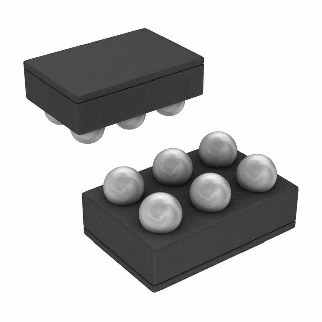
6-Bump Thin DSBGA Package
APPLICATIONS
•
•
Handsets, Tablets, Notebooks
Portable devices
Typical Application Circuit
VCC Main: 2.8V to 5.3V
1.8V
220k
220k
VCC
GND
POK
B1
C1
A2
LM34902
PC
A1
B2
C2
ACC_PWR
VIN
Accessory
Device
ENABLE
ACC_DET
1M
Accessory
Detection
1
2
Please be aware that an important notice concerning availability, standard warranty, and use in critical applications of
Texas Instruments semiconductor products and disclaimers thereto appears at the end of this data sheet.
All trademarks are the property of their respective owners.
PRODUCTION DATA information is current as of publication date.
Products conform to specifications per the terms of the Texas
Instruments standard warranty. Production processing does not
necessarily include testing of all parameters.
Copyright © 2012–2013, Texas Instruments Incorporated
�LM34902
SNVS804B – MAY 2012 – REVISED APRIL 2013
www.ti.com
Connection Diagram
Figure 1. Top View
6-Bump Thin DSBGA Package
See Package Number YFQ
PIN DESCRIPTION
Name
Pin
Number
VCC
A1
Power input of the PFET switch. It also provides power to the entire IC. Connect to the voltage rail that the
accessory device is expected to work off.
GND
B1
Common Ground (device substrate).
POK
C1
Open-drain PFET status indicator. When the PFET is off, this pin floats. When PFET is on, it is grounded.
ACC_DET
C2
Pull this pin low to tell the IC that the downstream accessory device is plugged in.
ENABLE
B2
When this pin is low, the PFET will be turned off and POK will be open-drained. Current limit circuitry will also
be disabled. The IC will be in a low-power state. This pin should be held low until VCC is established to
ensure proper initial state of internal logic. When ENABLE is high, the PFET switch will be allowed to turn on.
ACC_PWR
A2
Power output terminal of the PFET switch. Connect to input rail of accessory device.
Function
Truth Table
Input
Output
ENABLE
ACC_DET
Current Limit
Detected
TJ Limit
Exceeded
2.8V < VCC < 5.3V
PFET Switch
Status
POK
0
x
No
No
Yes
Open
Open Drain
x
1
No
No
Yes
Open
Open Drain
0 to 1
0
No
No
Yes
On
Grounded
0 to 1
0
Yes
No
Yes
Current Limited
Grounded
x
x
x
Yes
2.2V < VCC < 5.3V
Open
Open Drain
0
x
x
No
2.2V < VCC < 2.8V
Open
Open Drain
Note: "x" stands for "don't care".
These devices have limited built-in ESD protection. The leads should be shorted together or the device placed in conductive foam
during storage or handling to prevent electrostatic damage to the MOS gates.
Absolute Maximum Ratings (1)
VCC
-0.3V to 6V
ENABLE, POK, ACC_DET,
ACC_PWR (2)
-0.3V to 6V
Junction Temperature (TJ)
+150°C
−65°C to +150°C
Storage Temperature Range
ESD Susceptibility, Human Body Model (3)
(1)
(2)
(3)
2
2kV
Absolute Maximum Ratings are limits beyond which damage to the device may occur. Operating Ratings are conditions under which
operation of the device is ensured. Operating Ratings do not imply ensured performance limits. For ensured performance limits and
associated test conditions, see the Electrical Characteristics table.
The voltages on these pins should never exceed VCC+0.3V.
The human body model is a 100pF capacitor discharged through a 1.5 kΩ resistor into each pin. Test method is per JESD-22-A114.
Submit Documentation Feedback
Copyright © 2012–2013, Texas Instruments Incorporated
Product Folder Links: LM34902
�LM34902
www.ti.com
SNVS804B – MAY 2012 – REVISED APRIL 2013
Operating Ratings (1)
VCC Voltage (2)
2.8V to 5.3V
Junction Temperature (TJ), LM34902
(1)
-40°C to +85°C
Absolute Maximum Ratings are limits beyond which damage to the device may occur. Operating Ratings are conditions under which
operation of the device is ensured. Operating Ratings do not imply ensured performance limits. For ensured performance limits and
associated test conditions, see the Electrical Characteristics table.
For VCC between 2.2V and 2.8V, if ENABLE is a logic low, the LM34902 will not turn on the PFET switch.
(2)
Electrical Characteristics
Unless otherwise stated, the following conditions apply: VCC = 3V. Limits in standard type are for TJ = 25°C only; limits in
boldfacetype apply over the operating junction temperature (TJ) range. Minimum and Maximum limits are ensured through
test, design, or statistical correlation. Typical values represent the most likely parametric norm at TJ = 25°C and are provided
for reference purposes only.
Symbol
Parameter
Conditions
VIL
Input Low Voltage, ACC_DET,
ENABLE
VIH
Input High Voltage, ACC_DET,
ENABLE
VIHS
Input Hysteresis, ACC_DET,
ENABLE
ILK
Input Current, ACC_DET, ENABLE ACC_DET, ENABLE between 0V and VCC
Min
Typ
Max
Units
0.45
V
1.35
V
55
mV
1
µA
10
µA
47
100
µA
0.64
1
Ω
1
µA
0.65
A
0.4
V
1
µA
ISD
VCC Current in Shutdown Mode
VENABLE = 0V
VVCC = 5.3V
IQ
VCC Quiescent Current
VENABLE = 1.8V
VVCC = 5.3V, IACC_PWR = 0A
RON
Total On Resistance Between
VCC and ACC_PWR Pins
VVCC = 3V
IACC_PWR = 0.3A
ILK_ACC
ACC_PWR Leakage Current
When PFET is Off
VACC_PWR = 0V to VCC
VVCC = 5.3V
VENABLE = 0V
ILIMIT
PFET Switch Current Limit
VVCC = 2.8V to 5.3V
VACC_PWR = 0V
VPOK
POK Current Sink Capability
POK asserted. 1mA sink current.
IPOK
POK Leakage Current
POK de-asserted.
VPOK = 3.3V
T1
ACC_DET Response Time
ACC_DET rising to either PFET or POK FET
turn-off
40
ns
T2
ENABLE Response Time
ENABLE rising to either PFET or POK FET turnon
10
µs
T3
Minimum ENABLE Cycle Time (1)
ACC_DET tied to ground. ENABLE logic high =
1.8V. VCC = 2.8V to 5.3V.
300
ns
(1)
0.3
0.45
If ENABLE toggles low from a high state, it needs to stay low for at least T3 long before toggling back to high. Otherwise the internal flipflop may not be set and the PFET switch may not turn on.
Thermal Characteristics
Symbol
Description
Conditions
Typical
Value
Unit
θJA1
Junction-to-Ambient
Thermal Resistance
Mount device on a standard 4-layer 4" x 3" JEDEC board. Apply known amount of
power to the package. Measure junction temperature and surrounding air
temperature. No air flow. Refer to JESD51-7 for more information.
104
°C/W
θJA2
Junction-to-Ambient
Thermal Resistance
Mount device on a 2-layer 2.19" x 2.9" board. Copper thickness is 1 oz per layer.
No airflow. Power dissipation is 0.5W.
136
°C/W
TSD
Thermal Shutdown
Threshold
Raise TJ from below 150°C until POK is de-asserted. No load is connected at
ACC_PWR.
170
°C
Submit Documentation Feedback
Copyright © 2012–2013, Texas Instruments Incorporated
Product Folder Links: LM34902
3
�LM34902
SNVS804B – MAY 2012 – REVISED APRIL 2013
www.ti.com
Typical Performance Characteristics
Unless indicated otherwise, VCC = 3V and TJ = 25°C.
4
Total ON Resistance vs Temperature
Total ON Resistance vs Switch Current
Figure 2.
Figure 3.
Total ON Resistance vs VCC
Current Limit vs Temperature
Figure 4.
Figure 5.
Input Logic High Threshold vs Temperature
Input Logic Low Threshold vs Temperature
Figure 6.
Figure 7.
Submit Documentation Feedback
Copyright © 2012–2013, Texas Instruments Incorporated
Product Folder Links: LM34902
�LM34902
www.ti.com
SNVS804B – MAY 2012 – REVISED APRIL 2013
BLOCK DIAGRAM
APPLICATION HINTS
To turn on the PFET switch, both the ENABLE and the ACC_DET pins need to be asserted. In addition,
ACC_DET needs to be asserted no later than the rising edge of the ENABLE signal. De-assertion of either the
ENABLE or the ACC_DET will result in turned-off PFET switch and de-asserted POK signal.
To prevent a glitch in the otherwise asserted ACC_DET from keeping the FETs turned off, it is a good practice to
cycle the ENABLE following every falling edge in the ACC_DET signal. When cycling the ENABLE, make sure it
stays low for at least T3 long before toggling back high. If ENABLE logic high level is not 1.8V, make sure
ENABLE stays low for at least 1µs.
When laying out the PCB, try to keep the ENABLE and ACC_DET traces as short as possible and away from
noisy traces.
Submit Documentation Feedback
Copyright © 2012–2013, Texas Instruments Incorporated
Product Folder Links: LM34902
5
�LM34902
SNVS804B – MAY 2012 – REVISED APRIL 2013
www.ti.com
REVISION HISTORY
Changes from Revision A (April 2013) to Revision B
•
6
Page
Changed layout of National Data Sheet to TI format ............................................................................................................ 5
Submit Documentation Feedback
Copyright © 2012–2013, Texas Instruments Incorporated
Product Folder Links: LM34902
�PACKAGE OPTION ADDENDUM
www.ti.com
23-May-2025
PACKAGING INFORMATION
Orderable part number
(1)
Status
Material type
(1)
(2)
Package | Pins
Package qty | Carrier
RoHS
(3)
Lead finish/
Ball material
MSL rating/
Peak reflow
(4)
(5)
Op temp (°C)
Part marking
(6)
LM34902ITM/NOPB
Active
Production
DSBGA (YFQ) | 6
250 | SMALL T&R
Yes
SNAGCU
Level-1-260C-UNLIM
-40 to 85
K
LM34902ITM/NOPB.A
Active
Production
DSBGA (YFQ) | 6
250 | SMALL T&R
Yes
SNAGCU
Level-1-260C-UNLIM
-40 to 85
K
LM34902ITMX/NOPB
Active
Production
DSBGA (YFQ) | 6
3000 | LARGE T&R
Yes
SNAGCU
Level-1-260C-UNLIM
-40 to 85
K
LM34902ITMX/NOPB.A
Active
Production
DSBGA (YFQ) | 6
3000 | LARGE T&R
Yes
SNAGCU
Level-1-260C-UNLIM
-40 to 85
K
Status: For more details on status, see our product life cycle.
(2)
Material type: When designated, preproduction parts are prototypes/experimental devices, and are not yet approved or released for full production. Testing and final process, including without limitation quality assurance,
reliability performance testing, and/or process qualification, may not yet be complete, and this item is subject to further changes or possible discontinuation. If available for ordering, purchases will be subject to an additional
waiver at checkout, and are intended for early internal evaluation purposes only. These items are sold without warranties of any kind.
(3)
RoHS values: Yes, No, RoHS Exempt. See the TI RoHS Statement for additional information and value definition.
(4)
Lead finish/Ball material: Parts may have multiple material finish options. Finish options are separated by a vertical ruled line. Lead finish/Ball material values may wrap to two lines if the finish value exceeds the maximum
column width.
(5)
MSL rating/Peak reflow: The moisture sensitivity level ratings and peak solder (reflow) temperatures. In the event that a part has multiple moisture sensitivity ratings, only the lowest level per JEDEC standards is shown.
Refer to the shipping label for the actual reflow temperature that will be used to mount the part to the printed circuit board.
(6)
Part marking: There may be an additional marking, which relates to the logo, the lot trace code information, or the environmental category of the part.
Multiple part markings will be inside parentheses. Only one part marking contained in parentheses and separated by a "~" will appear on a part. If a line is indented then it is a continuation of the previous line and the two
combined represent the entire part marking for that device.
Important Information and Disclaimer:The information provided on this page represents TI's knowledge and belief as of the date that it is provided. TI bases its knowledge and belief on information provided by third parties, and
makes no representation or warranty as to the accuracy of such information. Efforts are underway to better integrate information from third parties. TI has taken and continues to take reasonable steps to provide representative
and accurate information but may not have conducted destructive testing or chemical analysis on incoming materials and chemicals. TI and TI suppliers consider certain information to be proprietary, and thus CAS numbers
and other limited information may not be available for release.
In no event shall TI's liability arising out of such information exceed the total purchase price of the TI part(s) at issue in this document sold by TI to Customer on an annual basis.
Addendum-Page 1
�PACKAGE MATERIALS INFORMATION
www.ti.com
5-Nov-2022
TAPE AND REEL INFORMATION
REEL DIMENSIONS
TAPE DIMENSIONS
K0
P1
B0 W
Reel
Diameter
Cavity
A0
B0
K0
W
P1
A0
Dimension designed to accommodate the component width
Dimension designed to accommodate the component length
Dimension designed to accommodate the component thickness
Overall width of the carrier tape
Pitch between successive cavity centers
Reel Width (W1)
QUADRANT ASSIGNMENTS FOR PIN 1 ORIENTATION IN TAPE
Sprocket Holes
Q1
Q2
Q1
Q2
Q3
Q4
Q3
Q4
User Direction of Feed
Pocket Quadrants
*All dimensions are nominal
Device
Package Package Pins
Type Drawing
SPQ
Reel
Reel
A0
Diameter Width (mm)
(mm) W1 (mm)
LM34902ITM/NOPB
DSBGA
YFQ
6
250
178.0
8.4
LM34902ITMX/NOPB
DSBGA
YFQ
6
3000
178.0
8.4
Pack Materials-Page 1
B0
(mm)
K0
(mm)
P1
(mm)
W
Pin1
(mm) Quadrant
0.89
1.3
0.7
4.0
8.0
Q1
0.89
1.3
0.7
4.0
8.0
Q1
�PACKAGE MATERIALS INFORMATION
www.ti.com
5-Nov-2022
TAPE AND REEL BOX DIMENSIONS
Width (mm)
W
L
H
*All dimensions are nominal
Device
Package Type
Package Drawing
Pins
SPQ
Length (mm)
Width (mm)
Height (mm)
LM34902ITM/NOPB
DSBGA
YFQ
LM34902ITMX/NOPB
DSBGA
YFQ
6
250
208.0
191.0
35.0
6
3000
208.0
191.0
35.0
Pack Materials-Page 2
�MECHANICAL DATA
YFQ0006xxx
D
0.600±0.075
E
TMD06XXX (Rev B)
D: Max = 1.24 mm, Min = 1.18 mm
E: Max = 0.84 mm, Min = 0.78 mm
4215075/A
NOTES:
A. All linear dimensions are in millimeters. Dimensioning and tolerancing per ASME Y14.5M-1994.
B. This drawing is subject to change without notice.
www.ti.com
12/12
�IMPORTANT NOTICE AND DISCLAIMER
TI PROVIDES TECHNICAL AND RELIABILITY DATA (INCLUDING DATA SHEETS), DESIGN RESOURCES (INCLUDING REFERENCE
DESIGNS), APPLICATION OR OTHER DESIGN ADVICE, WEB TOOLS, SAFETY INFORMATION, AND OTHER RESOURCES “AS IS”
AND WITH ALL FAULTS, AND DISCLAIMS ALL WARRANTIES, EXPRESS AND IMPLIED, INCLUDING WITHOUT LIMITATION ANY
IMPLIED WARRANTIES OF MERCHANTABILITY, FITNESS FOR A PARTICULAR PURPOSE OR NON-INFRINGEMENT OF THIRD
PARTY INTELLECTUAL PROPERTY RIGHTS.
These resources are intended for skilled developers designing with TI products. You are solely responsible for (1) selecting the appropriate
TI products for your application, (2) designing, validating and testing your application, and (3) ensuring your application meets applicable
standards, and any other safety, security, regulatory or other requirements.
These resources are subject to change without notice. TI grants you permission to use these resources only for development of an
application that uses the TI products described in the resource. Other reproduction and display of these resources is prohibited. No license
is granted to any other TI intellectual property right or to any third party intellectual property right. TI disclaims responsibility for, and you
will fully indemnify TI and its representatives against, any claims, damages, costs, losses, and liabilities arising out of your use of these
resources.
TI’s products are provided subject to TI’s Terms of Sale or other applicable terms available either on ti.com or provided in conjunction with
such TI products. TI’s provision of these resources does not expand or otherwise alter TI’s applicable warranties or warranty disclaimers for
TI products.
TI objects to and rejects any additional or different terms you may have proposed. IMPORTANT NOTICE
Mailing Address: Texas Instruments, Post Office Box 655303, Dallas, Texas 75265
Copyright © 2025, Texas Instruments Incorporated
�