LM34914
www.ti.com
SNVS453B – MAY 2006 – REVISED MARCH 2013
LM34914 Ultra Small 1.25A Step-Down Switching Regulator with Intelligent Current Limit
Check for Samples: LM34914
FEATURES
DESCRIPTION
•
•
•
The LM34914 Step-Down Switching Regulator
features all the functions needed to implement a low
cost, efficient, buck bias regulator capable of
supplying at least 1.25A to the load. To reduce
excessive switch current due to the possibility of a
saturating inductor the valley current limit threshold
changes with input and output voltages, and the ontime is reduced when current limit is detected. This
buck regulator contains a 44V N-Channel Buck
Switch, and is available in the thermally enhanced 3
mm x 3 mm WSON-10 package. The feedback
regulation scheme requires no loop compensation,
results in fast load transient response, and simplifies
circuit implementation. The operating frequency
remains constant with line and load variations due to
the inverse relationship between the input voltage
and the on-time. The valley current limit results in a
smooth transition from constant voltage to constant
current mode when current limit is detected, reducing
the frequency and output voltage, without the use of
foldback. Additional features include: VCC undervoltage lock-out, thermal shutdown, gate drive undervoltage lock-out, and maximum duty cycle limit.
1
2
•
•
•
•
•
•
•
•
•
•
Input Voltage Range: 8V to 40V
Integrated N-Channel Buck Switch
Valley Current Limit Varies with VIN and VOUT
to Reduce Excessive Inductor Current
On-time is Reduced when in Current Limit
Integrated Start-Up Regulator
No Loop Compensation Required
Ultra-Fast Transient Response
Maximum Switching Frequency: 1.3 MHz
Operating Frequency Remains Nearly
Constant with Load Current and Input Voltage
Variations
Programmable Soft-Start
Precision Internal Reference
Adjustable Output Voltage
Thermal Shutdown
TYPICAL APPLICATIONS
•
•
•
High Efficiency Point-Of-Load (POL) Regulator
Non-Isolated Buck Regulator
Secondary High Voltage Post Regulator
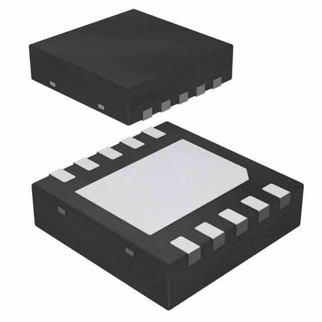
Package
•
•
WSON-10 (3 mm x 3mm)
Exposed Thermal Pad
Dissipation
For
Improved
Heat
Basic Step Down Regulator
8V - 40V
Input
VCC
VIN
C1
C3
LM34914
RON
BST
RON/SD
L1
C4
SHUT
DOWN
VOUT
SW
D1
SS
R1
R3
ISEN
C5
FB
RTN
C2
R2
SGND
1
2
Please be aware that an important notice concerning availability, standard warranty, and use in critical applications of
Texas Instruments semiconductor products and disclaimers thereto appears at the end of this data sheet.
All trademarks are the property of their respective owners.
PRODUCTION DATA information is current as of publication date.
Products conform to specifications per the terms of the Texas
Instruments standard warranty. Production processing does not
necessarily include testing of all parameters.
Copyright © 2006–2013, Texas Instruments Incorporated
�LM34914
SNVS453B – MAY 2006 – REVISED MARCH 2013
www.ti.com
Connection Diagram
1
2
3
4
5
10
SW
VIN
BST
VCC
ISEN
RON/SD
SGND
SS
RTN
FB
9
8
7
6
10-Lead WSON
PIN DESCRIPTIONS
Pin Number
Name
Description
Application Information
1
SW
Switching Node
Internally connected to the buck switch source. Connect to
the inductor, diode, and bootstrap capacitor.
2
BST
Boost pin for bootstrap capacitor
Connect a 0.022 µF capacitor from SW to this pin. The
capacitor is charged each off-time via an internal diode.
3
ISEN
Current sense
The re-circulating current flows out of this pin to the freewheeling diode.
4
SGND
Sense Ground
Re-circulating current flows into this pin to the current sense
resistor.
5
RTN
Circuit Ground
Ground for all internal circuitry other than the current limit
detection.
6
FB
Feedback input from the regulated
output
Internally connected to the regulation and over-voltage
comparators. The regulation level is 2.5V.
7
SS
Softstart
An internal current source charges an external capacitor to
2.5V, providing the softstart function.
8
RON/SD
On-time control and shutdown
An external resistor from VIN to this pin sets the buck switch
on-time. Grounding this pin shuts down the regulator.
9
VCC
Output from the startup regulator
Nominally regulated at 7.0V. Connect a 0.1 µF capacitor from
this pin to RTN. An external voltage (8V to 14V) can be
applied to this pin to reduce internal dissipation. An internal
diode connects VCC to VIN.
10
VIN
Input supply voltage
Operating input range is 8.0V to 40V.
EP
Exposed Pad
Exposed metal pad on the underside of the device. It is
recommended to connect this pad to the PC board ground
plane to aid in heat dissipation.
These devices have limited built-in ESD protection. The leads should be shorted together or the device placed in conductive foam
during storage or handling to prevent electrostatic damage to the MOS gates.
2
Submit Documentation Feedback
Copyright © 2006–2013, Texas Instruments Incorporated
Product Folder Links: LM34914
�LM34914
www.ti.com
SNVS453B – MAY 2006 – REVISED MARCH 2013
Absolute Maximum Ratings (1) (2)
VIN to RTN
44V
BST to RTN
52V
SW to RTN (Steady State)
-1.5V
BST to VCC
44V
VIN to SW
44V
BST to SW
14V
VCC to RTN
14V
SGND to RTN
-0.3V to +0.3V
Current out of ISEN
See text
SS to RTN
-0.3V to 4V
All Other Inputs to RTN
-0.3 to 7V
ESD Rating (3)
Human Body Model
2kV
Storage Temperature Range
-65°C to +150°C
JunctionTemperature
150°C
(1)
(2)
(3)
Absolute Maximum Ratings are limits beyond which damage to the device may occur. Operating Ratings are conditions under which
operation of the device is intended to be functional. For specifications and test conditions, see Electrical Characteristics.
If Military/Aerospace specified devices are required, please contact the Texas Instruments Sales Office/Distributors for availability and
specifications.
The human body model is a 100pF capacitor discharged through a 1.5kΩ resistor into each pin.
Operating Ratings (1)
VIN Voltage
8.0V to 40V
−40°C to + 125°C
Junction Temperature
(1)
Absolute Maximum Ratings are limits beyond which damage to the device may occur. Operating Ratings are conditions under which
operation of the device is intended to be functional. For specifications and test conditions, see Electrical Characteristics.
Electrical Characteristics
Limits in standard type are for TJ = 25°C only; limits in boldface type apply over the junction temperature (TJ) range of -40°C
to +125°C. Minimum and Maximum limits are specified through test, design, or statistical correlation. Typical values represent
the most likely parametric norm at TJ = 25°C, and are provided for reference purposes only. Unless otherwise stated the
following conditions apply: VIN = 12V, RON = 200kΩ (1) (2).
Symbol
Parameter
Conditions
Min
Typ
Max
Units
6.6
7.0
7.4
V
Start-Up Regulator, VCC
VCCReg
UVLOVCC
(1)
(2)
(3)
VCC regulated output
Vin > 9V
VIN-VCC dropout voltage
ICC = 0 mA,
VCC = UVLOVCC + 250 mV
1.3
V
VCC output impedance
(0 mA ≤ ICC ≤ 5 mA)
VIN = 8V
155
VIN = 40V
0.16
VCC current limit (3)
VCC = 0V
11
mA
VCC under-voltage lockout
threshold
VCC increasing
5.7
V
UVLOVCC hysteresis
VCC decreasing
150
mV
UVLOVCC filter delay
100 mV overdrive
IIN operating current
Non-switching, FB = 3V
IIN shutdown current
RON/SD = 0V
Ω
3
µs
0.57
0.85
mA
80
160
µA
For detailed information on soldering plastic WSON packages, visit www.ti.com/packaging.
Typical specifications represent the most likely parametric norm at 25°C operation.
VCC provides self bias for the internal gate drive and control circuits. Device thermal limitations limit external loading
Submit Documentation Feedback
Copyright © 2006–2013, Texas Instruments Incorporated
Product Folder Links: LM34914
3
�LM34914
SNVS453B – MAY 2006 – REVISED MARCH 2013
www.ti.com
Electrical Characteristics (continued)
Limits in standard type are for TJ = 25°C only; limits in boldface type apply over the junction temperature (TJ) range of -40°C
to +125°C. Minimum and Maximum limits are specified through test, design, or statistical correlation. Typical values represent
the most likely parametric norm at TJ = 25°C, and are provided for reference purposes only. Unless otherwise stated the
following conditions apply: VIN = 12V, RON = 200kΩ(1)(2).
Symbol
Parameter
Conditions
Min
Typ
Max
Units
0.33
0.7
Ω
4.2
5.5
V
Switch Characteristics
Rds(on)
Buck Switch Rds(on)
ITEST = 200 mA
UVLOGD
Gate Drive UVLO
VBST - VSW Increasing
3.0
UVLOGD hysteresis
470
mV
VSS
Pull-up voltage
2.5
V
ISS
Internal current source
12.5
µA
Softstart Pin
Current Limit
ILIM
Threshold
VIN = 8V, VFB = 2.4V
1.0
1.2
1.4
VIN = 30V, VFB = 2.4V
0.9
1.1
1.3
VIN = 30V, VFB = 1.0V
0.85
1.05
1.25
Response time
150
A
ns
On Timer
tON - 1
On-time (normal operation)
VIN = 10V, RON = 200 kΩ
tON - 2
On-time (normal operation)
VIN = 40V, RON = 200 kΩ
2.1
655
ns
tON - 3
On-time (current limit)
VIN = 10V, RON = 200 kΩ
1.13
µs
Shutdown threshold at RON/SD
Voltage at RON/SD rising
Shutdown Threshold hysteresis
Voltage at RON/SD falling
0.4
2.8
0.8
3.4
1.2
µs
V
32
mV
265
ns
Off Timer
tOFF
Minimum Off-time
Regulation and Over-Voltage Comparators (FB Pin)
VREF
FB regulation threshold
SS pin = steady state
2.445
2.50
2.550
V
FB over-voltage threshold
2.9
V
FB bias current
15
nA
175
°C
20
°C
Thermal Shutdown
TSD
Thermal shutdown temperature
Junction temperature rising
Thermal shutdown hysteresis
Thermal Resistance
(4)
4
θJA
Junction to Ambient
0 LFPM Air Flow (4)
30
°C/W
θJC
Junction to Case (4)
8
°C/W
Value shown assumes a 4-layer PC board and 4 vias to conduct heat from beneath the package.
Submit Documentation Feedback
Copyright © 2006–2013, Texas Instruments Incorporated
Product Folder Links: LM34914
�LM34914
www.ti.com
SNVS453B – MAY 2006 – REVISED MARCH 2013
Typical Performance Characteristics
Unless otherwise specified the following conditions apply: TJ = 25°C
Typical Efficiency Performance
VCC vs VIN
100
7.5
Vin = 8V
95
90
24V
VCC (V)
EFFICIENCY (%)
7.0
12V
85
40V
80
75
6.5
6.0
5.5
VOUT = 5V
FS = 275 kHz
70
0
200
400
600
800
5.0
1000
6.5
7.0
7.5
8.0
8.5
9.0
LOAD CURRENT (mA)
VIN (V)
Figure 1.
Figure 2.
VCC vs ICC
ON-Time vs VIN and RON
8
10
VIN = 9V
6
ON-TIME (Ps)
4
3
2
600k
200k
3.0
VIN = 8V
5
VCC (V)
400k
VIN t 10V
7
100k
1.0
0.3
VCC Externally Loaded
1
RON = 45k
FS = 200 kHZ
0.1
0
2
0
4
8
6
ICC (mA)
10
0
12
10
Figure 3.
20
VIN (V)
40
30
Figure 4.
Valley Current Limit Threshold
vs. FB and VIN
Voltage at the RON/SD Pin
3.0
1.3
1.2
VIN = 8V
15V
24V
1.1
34V
1.0
40V
RON/SD PIN VOLTAGE (V)
VALLEY CURRENT
LIMIT THRESHOLD (A)
RON = 45k
100k
2.0
500k
1.0
0
0.9
0
0.5
1.0
1.5
2.0
2.5
0
10
20
30
40
VIN (V)
VFB (V)
Figure 5.
Figure 6.
Submit Documentation Feedback
Copyright © 2006–2013, Texas Instruments Incorporated
Product Folder Links: LM34914
5
�LM34914
SNVS453B – MAY 2006 – REVISED MARCH 2013
www.ti.com
Typical Performance Characteristics (continued)
Unless otherwise specified the following conditions apply: TJ = 25°C
Input Shutdown and Operating Current Into VIN
INPUT CURRENT (PA)
800
600
Operating Current
400
200
Shutdown Current
0
0
10
20
30
40
VIN (V)
Figure 7.
6
Submit Documentation Feedback
Copyright © 2006–2013, Texas Instruments Incorporated
Product Folder Links: LM34914
�LM34914
www.ti.com
SNVS453B – MAY 2006 – REVISED MARCH 2013
Typical Application Circuit and Block Diagram
Input
8V - 40V
7V START-UP
REGULATOR
VIN
C5
LM34914
VCC
VCC
THERMAL
SHUTDOWN
C3
UVLO
C1
ON TIMER
GND
RON
RON
START
' Ton FINISH
RON/SD
MINIMUM
OFF TIMER
START FINISH
0.8V
BST
Gate Drive SD
UVLO
2.5V
SS
12.5 PA
VIN
C4
LOGIC
LEVEL
SHIFT
Driver
C6
L1
SW
FB
REGULATION
COMPARATOR
2.9V
VOUT
D1
OVER-VOLTAGE
COMPARATOR
CURRENT LIMIT
COMPARATOR
+
-
RTN
VIN
FB
CL
Threshold
Adjust
RSENSE
+
ISEN
R1
R3
R2
C2
41 m:
SGND
Submit Documentation Feedback
Copyright © 2006–2013, Texas Instruments Incorporated
Product Folder Links: LM34914
7
�LM34914
SNVS453B – MAY 2006 – REVISED MARCH 2013
www.ti.com
VIN
7.0V
UVLO
VCC
SW Pin
Inductor
Current
2.5V
SS Pin
VOUT
t1
t2
Figure 8. Startup Sequence
Functional Description
The LM34914 Step Down Switching Regulator features all the functions needed to implement a low cost, efficient
buck bias power converter capable of supplying at least 1.25A to the load. This high voltage regulator contains
an N-Channel buck switch, is easy to implement, and is available in the thermally enhanced 3mm x 3mm WSON10 package. The regulator’s operation is based on a constant on-time control scheme where the on-time is
determined by VIN. This feature results in the operating frequency remaining relatively constant with load and
input voltage variations. The feedback control scheme requires no loop compensation resulting in very fast load
transient response. The valley current limit scheme protects against excessively high currents if the output is
short circuited when VIN is high. To aid in controlling excessive switch current due to a possible saturating
inductor the valley current limit threshold changes with input and output voltages, and the on-time is reduced by
approximately 50% when current limit is detected.The LM34914 can be applied in numerous applications to
efficiently regulate down higher voltages. Additional features include: Thermal shutdown, VCC under-voltage lockout, gate drive under-voltage lock-out, and maximum duty cycle limit.
Control Circuit Overview
The LM34914 buck DC-DC regulator employs a control scheme based on a comparator and a one-shot on-timer,
with the output voltage feedback (FB) compared to an internal reference (2.5V). If the FB voltage is below the
reference the buck switch is switched on for a time period determined by the input voltage and a programming
resistor (RON). Following the on-time the switch remains off until the FB voltage falls below the reference, but not
less than the minimum off-time forced by the LM34914. The buck switch is then turned on for another on-time
period.
8
Submit Documentation Feedback
Copyright © 2006–2013, Texas Instruments Incorporated
Product Folder Links: LM34914
�LM34914
www.ti.com
SNVS453B – MAY 2006 – REVISED MARCH 2013
When in regulation, the LM34914 operates in continuous conduction mode at heavy load currents and
discontinuous conduction mode at light load currents. In continuous conduction mode the inductor’s current is
always greater than zero, and the operating frequency remains relatively constant with load and line variations.
The minimum load current for continuous conduction mode is one-half the inductor’s ripple current amplitude.
The approximate operating frequency is calculated as follows:
FS =
VOUT x (VIN ± 1.5)
1.15 x 10⁻¹⁰ x (RON + 1.4k) x VIN
(1)
The buck switch duty cycle is equal to:
DC =
VOUT
tON
tON + tOFF
= tON x FS =
VIN
(2)
In discontinuous conduction mode, where the inductor’s current reaches zero during the off-time forcing a longerthan-normal off-time, the operating frequency is lower than in continuous conduction mode, and varies with load
current. Conversion efficiency is maintained at light loads since the switching losses decrease with the reduction
in load and frequency. The approximate discontinuous operating frequency can be calculated as follows:
FS =
VOUT2 x L1 x 1.5 x 1020
RL x RON2
(3)
where RL = the load resistance, and L1 is the circuit’s inductor.
The output voltage is set by the two feedback resistors (R1, R2 in the Block Diagram). The regulated output
voltage is calculated as follows:
VOUT = 2.5 x (R1 + R2) / R2
(4)
Output voltage regulation is based on supplying ripple voltage to the feedback input (FB pin), normally obtained
from the output voltage ripple through the feedback resistors. The LM34914 requires a minimum of 25 mVp-p of
ripple voltage at the FB pin, requiring the ripple voltage at VOUT be higher by the gain factor of the feedback
resistor ratio. The output ripple voltage is created by the inductor’s ripple current passing through R3 which is in
series with the output capacitor. For applications where reduced ripple is required at VOUT, see Applications
Information.
If the voltage at FB rises above 2.9V, due to a transient at VOUT or excessive inductor current which creates
higher than normal ripple at VOUT, the internal over-voltage comparator immediately shuts off the internal buck
switch. The next on-time starts when the voltage FB falls below 2.5V and the inductor current falls below the
current limit threshold.
ON-Time Timer
The on-time for the LM34914 is determined by the RON resistor and the input voltage (VIN), calculated from:
1.15 x 10
tON =
-10
x (RON + 1.4k)
(VIN - 1.5)
+ 50 ns
(5)
The inverse relationship with VIN results in a nearly constant frequency as VIN is varied. To set a specific
continuous conduction mode switching frequency (FS), the RON resistor is determined from the following:
VOUT x (VIN - 1.5)
- 1.4k
RON =
-10
FS x 1.15 x 10 x VIN
(6)
Equation 1, Equation 5, and Equation 6 are valid only during normal operation - i.e., the circuit is not in current
limit. When the LM34914 operates in current limit, the on-time is reduced by approximately 50%. This feature
reduces the peak inductor current which may be excessively high if the load current and the input voltage are
simultaneously high. This feature operates on a cycle-by-cycle basis until the load current is reduced and the
output voltage resumes its normal regulated value.
Submit Documentation Feedback
Copyright © 2006–2013, Texas Instruments Incorporated
Product Folder Links: LM34914
9
�LM34914
SNVS453B – MAY 2006 – REVISED MARCH 2013
www.ti.com
Shutdown
The LM34914 can be remotely shut down by taking the RON/SD pin below 0.8V. See Figure 9. In this mode the
SS pin is internally grounded, the on-timer is disabled, and bias currents are reduced. Releasing the RON/SD pin
allows the circuit to resume operation. The voltage at the RON/SD pin is normally between 1.5V and 3.0V,
depending on VIN and the RON resistor.
VIN
Input
Voltage
RON
LM34914
RON/SD
STOP
RUN
Figure 9. Shutdown Implementation
Current Limit
Current limit detection occurs during the off-time by monitoring the recirculating current flowing out of the ISEN
pin. Referring to the Typical Application Circuit and Block Diagram, during the off-time the inductor current flows
through the load, into SGND, through the internal sense resistor, out of ISEN and through D1 to the inductor. If
that current exceeds the current limit threshold the current limit comparator output delays the start of the next ontime period. The next on-time starts when the current out of ISEN is below the threshold and the voltage at FB
falls below 2.5V. The operating frequency is typically lower due to longer-than-normal off-times.
The valley current limit threshold is a function of the input voltage (VIN) and the output voltage sensed at FB, as
shown in the graph “Valley Current Limit Threshold vs. VFB and VIN”. This feature reduces the inductor current’s
peak value at high line and load. To further reduce the inductor’s peak current, the next cycle’s on-time is
reduced by approximately 50% if the voltage at FB is below its threshold when the inductor current reduces to
the current limit threshold (VOUT is low due to current limiting).
Figure 10 illustrates the inductor current waveform during normal operation and in current limit. During the first
“Normal Operation” the load current is IOUT1, the average of the ripple waveform. As the load resistance is
reduced, the inductor current increases until it exceeds the current limit threshold. During the “Current Limited”
portion of Figure 10, the current limit threshold lowers since the high load current causes VOUT (and the voltage
at FB) to reduce. The on-time is reduced by approximately 50%, resulting in lower ripple amplitude for the
inductor’s current. During this time the LM34914 is in a constant current mode, with an average load current
equal to the current limit threshold + ΔI/2 (IOUT2). Normal operation resumes when the load current is reduced to
IOUT3, allowing VOUT, the current limit threshold, and the on-time to return to their normal values. Note that in the
second period of “Normal Operation”, even though the inductor’s peak current exceeds the current limit threshold
during part of each cycle, the circuit is not in current limit since the current falls below the threshold before the
feedback voltage reduces to its threshold.
The peak current allowed through the buck switch, and the ISEN pin, is 2A, and the maximum allowed average
current is 1.5A.
10
Submit Documentation Feedback
Copyright © 2006–2013, Texas Instruments Incorporated
Product Folder Links: LM34914
�LM34914
www.ti.com
SNVS453B – MAY 2006 – REVISED MARCH 2013
Inductor Current
IOUT2
Current Limit
Threshold
IOUT3
TON
'I
2
IOUT1
Feedback
Voltage
@ FB Pin
TON
2.5V
Normal
Operation
Load
Current
Increases
Current
Limited
Normal
Operation
Load Current
Decreases
Figure 10. Inductor Current - Normal and Current Limit Operation
N - Channel Buck Switch and Driver
The LM34914 integrates an N-Channel buck switch and associated floating high voltage gate driver. The gate
driver circuit works in conjunction with an external bootstrap capacitor and an internal high voltage diode. A 0.022
µF capacitor (C4) connected between BST and SW provides the voltage to the driver during the on-time. During
each off-time, the SW pin is at approximately -1V, and C4 is recharged for the next on-time from VCC through the
internal diode. The minimum off-time ensures a minimum time each cycle to recharge the bootstrap capacitor.
Softstart
The softstart feature allows the converter to gradually reach a steady state operating point, thereby reducing
start-up stresses and current surges. Upon turn-on, after VCC reaches the under-voltage threshold, an internal
12.5 µA current source charges up the external capacitor at the SS pin to 2.5V (t2 in Figure 8). The ramping
voltage at SS (and the non-inverting input of the regulation comparator) ramps up the output voltage in a
controlled manner.
An internal switch grounds the SS pin if VCC is below the under-voltage lockout threshold, or if the RON/SD pin is
grounded.
Thermal Shutdown
The LM34914 should be operated so the junction temperature does not exceed 125°C. If the junction
temperature increases above that, an internal Thermal Shutdown circuit activates (typically) at 175°C, taking the
controller to a low power reset state by disabling the buck switch and the on-timer. This feature helps prevent
catastrophic failures from accidental device overheating. When the junction temperature reduces below 155°C
(typical hysteresis = 20°C), normal operation resumes.
Submit Documentation Feedback
Copyright © 2006–2013, Texas Instruments Incorporated
Product Folder Links: LM34914
11
�LM34914
SNVS453B – MAY 2006 – REVISED MARCH 2013
www.ti.com
APPLICATIONS INFORMATION
EXTERNAL COMPONENTS
The following guidelines can be used to select the external components (see the Block Diagram). First determine
the following operating parameters:
- Output voltage (VOUT)
- Minimum and maximum input voltage (VIN(min) and VIN(max))
- Minimum and maximum load current (IOUT(min) and IOUT(max))
- Switching Frequency (FS)
R1 and R2: These resistors set the output voltage. The ratio of these resistors is calculated from:
R1/R2 = (VOUT/2.5V) - 1
(7)
R1 and R2 should be chosen from standard value resistors in the range of 1.0 kΩ - 10 kΩ which satisfy the
above ratio.
RON: The resistor sets the on-time, and consequently, the switching frequency. Its value can be determined using
Equation 6 based on the frequency, or Equation 5 if a specific on-time is required. The minimum allowed value
for RON is calculated from:
RON t
100 ns x (VIN(MAX) ± 1.5V)
1.15 x 10⁻¹⁰
- 1.4 k:
(8)
L1: The main parameter affected by the inductor is the output current ripple amplitude (IOR). The minimum load
current is used to determine the maximum allowable ripple. In order to maintain continuous conduction mode the
valley should not reach 0 mA. This is not a requirement of the LM34914, but serves as a guideline for selecting
L1. For this case, the maximum ripple current is:
IOR(MAX) = 2 x IOUT(min)
(9)
If the minimum load current is zero, use 20% of IOUT(max) for IOUT(min) in Equation 9. The ripple calculated in
Equation 6 is then used in the following equation:
VOUT x (VIN (max) - VOUT)
L1 =
IOR (max) x FS x VIN (max)
(10)
where Fs is the switching frequency. This provides a minimum value for L1. The next larger standard value
should be used, and L1 should be rated for the peak current level, equal to IOUT(max) + IOR(max)/2.
C2 and R3: Since the LM34914 requires a minimum of 25 mVp-p of ripple at the FB pin for proper operation, the
required ripple at VOUT is increased by R1 and R2. This necessary ripple is created by the inductor ripple current
flowing through R3, and to a lesser extent by C2 and its ESR. The minimum inductor ripple current is calculated
using Equation 10, rearranged to solve for IOR at minimum VIN.
VOUT x (VIN (min) - VOUT)
IOR (min) =
L1 x FS x VIN (min)
(11)
The minimum value for R3 is then equal to:
R3(min) =
25 mV x (R1 + R2)
R2 x IOR (min)
(12)
Typically R3 is less than 5Ω. C2 should generally be no smaller than 3.3 µF, although that is dependent on the
frequency and the desired output characteristics. C2 should be a low ESR good quality ceramic capacitor.
Experimentation is usually necessary to determine the minimum value for C2, as the nature of the load may
require a larger value. A load which creates significant transients requires a larger value for C2 than a nonvarying load.
12
Submit Documentation Feedback
Copyright © 2006–2013, Texas Instruments Incorporated
Product Folder Links: LM34914
�LM34914
www.ti.com
SNVS453B – MAY 2006 – REVISED MARCH 2013
D1: A Schottky diode is recommended. Ultra-fast recovery diodes are not recommended as the high speed
transitions at the SW pin may inadvertently affect the IC’s operation through external or internal EMI. The diode
should be rated for the maximum input voltage (VIN(max)), the maximum load current (IOUT(max)), and the peak
current which occurs when the current limit and maximum ripple current are reached simultaneously. The diode’s
average power dissipation is calculated from:
PD1 = VF x IOUT x (1-D)
(13)
where VF is the diode's forward voltage drop, and D is the duty cycle.
C1 and C5: C1’s purpose is to supply most of the switch current during the on-time, and limit the voltage ripple
at VIN, on the assumption that the voltage source feeding VIN has an output impedance greater than zero. If the
source’s dynamic impedance is high (effectively a current source), it supplies the average input current, but not
the ripple current.
At maximum load current, when the buck switch turns on, the current into VIN suddenly increases to the lower
peak of the inductor’s ripple current, ramps up to the upper peak, then drop to zero at turn-off. The average
current during the on-time is the load current. For a worst case calculation, C1 must supply this average load
current during the maximum on-time. C1 is calculated from:
IOUT (max) x tON
C1 =
'V
(14)
where tON is the maximum on-time, and ΔV is the allowable ripple voltage at VIN. C5’s purpose is to help avoid
transients and ringing due to long lead inductance leading to the VIN pin. A low ESR, 0.1 µF ceramic chip
capacitor is recommended, and must be located close to the VIN and RTN pins.
C3: The capacitor at the VCC output provides not only noise filtering and stability, but also prevents false
triggering of the VCC UVLO at the buck switch on/off transitions. C3 should be no smaller than 0.1 µF, and should
be a good quality, low ESR, ceramic capacitor. C3’s value, and the VCC current limit, determine a portion of the
turn-on-time (t1 in Figure 8).
C4: The recommended value for C4 is 0.022 µF. A high quality ceramic capacitor with low ESR is recommended
as C4 supplies a surge current to charge the buck switch gate at turn-on. A low ESR also helps ensure a
complete recharge during each off-time.
C6: The capacitor at the SS pin determines the softstart time, i.e. the time for the output voltage, to reach its final
value (t2 in Figure 8). The capacitor value is determined from the following:
C6 =
t2 x 12.5 PA
2.5V
(15)
PC BOARD LAYOUT
The LM34914 regulation, over-voltage, and current limit comparators are very fast, and respond to short duration
noise pulses. Layout considerations are therefore critical for optimum performance. The layout must be as neat
and compact as possible, and all of the components must be as close as possible to their associated pins. The
current loop formed by D1, L1, C2 and the SGND and ISEN pins should be as small as possible. The ground
connection from SGND and RTN to C1 should be as short and direct as possible.
If it is expected that the internal dissipation of the LM34914 will produce excessive junction temperatures during
normal operation, good use of the PC board’s ground plane can help to dissipate heat. The exposed pad on the
bottom of the IC package can be soldered to a ground plane, and that plane should extend out from beneath the
IC, and be connected to ground plane on the board’s other side with several vias, to help dissipate the heat. The
exposed pad is internally connected to the IC substrate. Additionally the use of wide PC board traces, where
possible, can help conduct heat away from the IC. Judicious positioning of the PC board within the end product,
along with the use of any available air flow (forced or natural convection) can help reduce the junction
temperatures.
Submit Documentation Feedback
Copyright © 2006–2013, Texas Instruments Incorporated
Product Folder Links: LM34914
13
�LM34914
SNVS453B – MAY 2006 – REVISED MARCH 2013
www.ti.com
LOW OUTPUT RIPPLE CONFIGURATIONS
For applications where low output ripple is required, the following options can be used to reduce or nearly
eliminate the ripple.
a) Reduced ripple configuration: In Figure 11, Cff is added across R1 to AC-couple the ripple at VOUT directly
to the FB pin. This allows the ripple at VOUT to be reduced to a minimum of 25 mVp-p by reducing R3, since the
ripple at VOUT is not attenuated by the feedback resistors. The minimum value for Cff is determined from:
Cff =
tON (max)
(R1//R2)
(16)
where tON(max) is the maximum on-time, which occurs at VIN(min). The next larger standard value capacitor should
be used for Cff. R1 and R2 should each be towards the upper end of the 1kΩ to 10kΩ range.
L1
SW
VOUT
LM34914
Cff
R1
R3
FB
R2
C2
Figure 11. Reduced Ripple Configuration
b) Minimum ripple configuration: If the application requires a lower value of ripple (