LM3508
www.ti.com
SNVS494C – APRIL 2007 – REVISED MAY 2013
LM3508 Synchronous Magnetic Constant Current White LED Driver
Check for Samples: LM3508
FEATURES
DESCRIPTION
•
•
•
•
The LM3508 is a synchronous boost converter (no
external Schottky diode required) that provides a
constant current output. It is designed to drive up to 4
series white LEDs at 30mA from a single-cell Li-Ion
battery. A single low power external resistor is used
to set the maximum LED current. The LED current
can be adjusted by applying a PWM signal of up to
100kHz to the DIM pin. Internal soft-start circuitry is
designed to eliminate high in-rush current at start-up.
For maximum safety, the device features an
advanced short-circuit protection when the output is
shorted to ground. Additionally, over-voltage
protection and an 850kHz switching frequency allow
for the use of small, low-cost output capacitors with
lower voltage ratings. During shutdown, the output is
disconnected from the input preventing a leakage
current path through the LEDs to ground. The
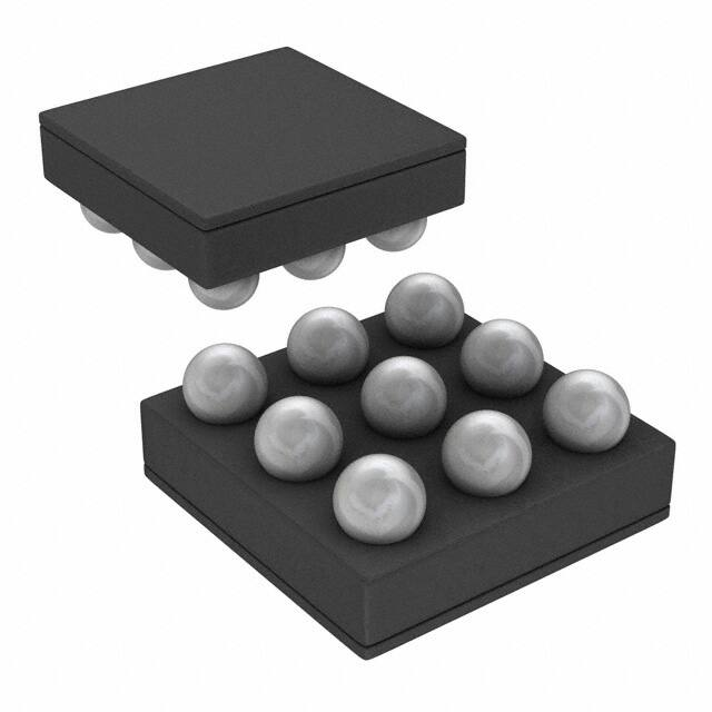
LM3508 is available in a tiny 9-bump chip-scale
DSBGA package.
1
2
•
•
•
•
•
•
•
•
Drives 4 Series White LEDs with up to 30mA
>80% Peak Efficiency
Up to 100kHz PWM Brightness Control
Accurate ±5% LED Current Regulation across
VIN range
Internal Synchronous PFET (No Schottky
Diode Required)
True Shutdown Isolation
Output Short-Circuit Protection
17.5V Over-Voltage Protection
Internal Soft-Start Eliminates Inrush Current
Wide Input Voltage Range: 2.7V to 5.5V
850kHz Fixed Frequency Operation
Low Profile 9-Bump DSBGA Package
(1.514mm x 1.514mm x 0.6mm)
APPLICATIONS
•
•
•
•
White LED Backlighting
Handheld Devices
Digital Cameras
Portable Applications
Typical Application Circuit
22 PH
SW
+
2.7V to 5.5V
OUT
IN
-
1 PF
EN
1 PF
LM3508
DIM
PWM Input
ILED
SET
AGND
PGND
RSET
1
2
Please be aware that an important notice concerning availability, standard warranty, and use in critical applications of
Texas Instruments semiconductor products and disclaimers thereto appears at the end of this data sheet.
All trademarks are the property of their respective owners.
PRODUCTION DATA information is current as of publication date.
Products conform to specifications per the terms of the Texas
Instruments standard warranty. Production processing does not
necessarily include testing of all parameters.
Copyright © 2007–2013, Texas Instruments Incorporated
�LM3508
SNVS494C – APRIL 2007 – REVISED MAY 2013
www.ti.com
Connection Diagram
A1
A2
A3
B1
B2
B3
C1
C2
C3
9-Bump (Large) DSBGA
(1.514mm x 1.514mm x 0.6mm) Package Number YZR000911A
Top View
PIN DESCRIPTIONS
Pin
Name
A1
PGND
Function
A2
SW
Inductor connection and drain connection for both NMOS and PMOS power devices.
A3
OUT
Output capacitor connection, PMOS source connection for synchronous rectifier, and OVP sensing
node.
B1
ILED
Regulated current source input.
B2
DIM
Current source modulation input. A logic low at DIM turns off the internal current source. A logic high
turns the LEDs fully on (VSET=200mV). Apply a PWM signal at DIM for LED brightness control.
Power Ground Connection.
B3
IN
C1
SET
Input voltage connection.
Current sense connection and current source output. Connect a 1% resistor (RSET) from SET to
PGND to set the maximum LED current (ILED = 200mV/RSET) .
C2
EN
Enable input. A logic low at EN turns off the LM3508. A logic high turns the device on.
C3
AGND
Analog ground. Connect AGND to PGND through a low impedance connection.
These devices have limited built-in ESD protection. The leads should be shorted together or the device placed in conductive foam
during storage or handling to prevent electrostatic damage to the MOS gates.
2
Submit Documentation Feedback
Copyright © 2007–2013, Texas Instruments Incorporated
Product Folder Links: LM3508
�LM3508
www.ti.com
SNVS494C – APRIL 2007 – REVISED MAY 2013
ABSOLUTE MAXIMUM RATINGS (1) (2) (3)
−0.3V to 6V
VIN
VOUT
−0.3V to 22V
VSW
−0.3V to 22V
−0.3V to 6V
VILED, VSET, VDIM, VEN
Continuous Power Dissipation
Internally Limited
Junction Temperature
+150°C
Lead Temperature (4)
+300°C
Storage Temperature Range
-65°C to +150°C
ESD Rating (5)
Human Body Model
(1)
(2)
(3)
(4)
(5)
2kV
Absolute maximum ratings are limits beyond which damage to the device may occur. Operating Ratings are conditions for which the
device is intended to be functional, but device parameter may not be specified. For specifications and test conditions, see the Electrical
Characteristics.
All voltages are with respect to PGND.
If Military/Aerospace specified devices are required, please contact the TI Sales Office/Distributors for availability and specifications.
For more detailed soldering information and specifications, please refer to Texas Instruments' Application Note AN-1112: DSBGA Wafer
Level Chip Scale Package (Literature Number SNVA009).
The human body model is a 100pF capacitor discharged through 1.5kΩ resistor into each pin. (MIL-STD-883 3015.7).
OPERATING CONDITIONS (1) (2)
Input Voltage Range
2.7V to 5.5V
Ambient Temperature Range (3)
−30°C to +85°C
−30°C to +105°C
Junction Temperature Range
(1)
(2)
(3)
Absolute maximum ratings are limits beyond which damage to the device may occur. Operating Ratings are conditions for which the
device is intended to be functional, but device parameters may not be specified. For specifications and test conditions, see the Electrical
Characteristics.
All voltages are with respect to PGND.
In applications where high power dissipation and/or poor package thermal resistance is present, the maximum ambient temperature may
have to be derated. Maximum ambient temperature (TA-MAX) is dependent on the maximum operating junction temperature (TJ-MAX-OP =
+125ºC), the maximum power dissipation of the device in the application (PD-MAX), and the junction-to ambient thermal resistance of the
part/package in the application (θJA), as given by the following equation: TA-MAX = TJ-MAX-OP – (θJA × PD-MAX).
THERMAL PROPERTIES
Junction to Ambient Thermal Resistance (θJA) (1)
(1)
64.7°C/W
Junction-to-ambient thermal resistance (θJA) is taken from thermal modeling performed under the conditions and guidelines set forth in
the JEDEC standard JESD51-7. The test board is a 4-layer FR-4 board mesuring (102mm × 76mm × 1.6mm) with a 2 × 1 array of
thermal vias. The ground plane on the board is (50mm × 50mm). Thickness of copper layers are (36µm/18µm/18µm/36µm)
(1.5oz/1oz/1oz/1.5oz copper). Ambient temperature in simulation is +22°C, still air. Power dissipation is 1W.
Submit Documentation Feedback
Copyright © 2007–2013, Texas Instruments Incorporated
Product Folder Links: LM3508
3
�LM3508
SNVS494C – APRIL 2007 – REVISED MAY 2013
www.ti.com
ELECTRICAL CHARACTERISTICS
Specifications in standard type face are for TA = 25°C and those in boldface type apply over the Operating Temperature
Range of TA = −30°C to +85°C. Unless otherwise specified VIN =3.6V. (1)
Symbol
ID
Parameter
Conditions
Min
Typ
LED Current
Regulation
RSET = 10Ω
20
RSET = 6.67Ω
30
VSET
Voltage at SET Pin
3.0V < VIN < 5.5V
VILED
Voltage at ILED Pin
VHR
Current Sink
Headroom Voltage
RDSON
200
mA
210
mV
mV
Where ILED = 95% of
nominal, RSET = 20Ω
400
mV
NMOS Switch On
Resistance
ISW = 100mA
0.5
PMOS Switch On
Resistance
VOUT = 10V, ISW = 65mA
2.2
NMOS Switch Current
Limit
ILSW
SW Leakage Current
VSW = VIN = 5.5V, OUT
Floating, VEN = PGND
IOUT_SHUTDOWN
Outout Pull-Down
Resistance in
Shutdown
VEN = 0V
Output Over-Voltage
Protection
ON Threshold (VOUT rising)
fSW
Switching Frequency
DMAX
Maximum Duty Cycle
VSC
Output Voltage
Threshold for Short
Circuit Detection
Ω
370
17.5
OFF Threshold (VOUT
falling)
3.0V < VIN < 5.5V
500
µA
630
Ω
19.8
850
0.93×VIN
VOUT Rising
0.95×VIN
VDIM_TH
DIM Threshold
Voltage
V
1150
On Threshold
kHz
%
V
1.1
Off Threshold
0.5
1.1
Off Threshold
(2)
21.8
18.6
715
mA
0.01
VOUT Falling
EN Threshold Voltage On Threshold
DIM Bias Current (2)
620
91
VEN_TH
IDIM
Units
500
ICL
VOVP
190
Max
0.5
V
V
VDIM = 1.8V
4.7
µA
IEN
EN Bias Current
VEN = 1.8V
4.7
µA
IOUT
OUT Bias Current
VOUT = 16V, device not
switching
420
µA
ROUT_SHUTDOWN
Output Pull-Down
Resistance in
Shutdown
VEN = 0V, VOUT < VIN
630
Ω
Quiescent Current
Device Not Switching
VILED > 0.5V, 3.0V < VIN <
5.5V, SW Floating
0.18
0.3
VEN = 0V, 3.0V < VIN <
5.5V
0.01
0.5
IQ
IQ_SW
Switching Supply
Current
tSTART_UP
From EN Low to High
to Inductor Current
Steady State
(1)
(2)
4
mA
825
µA
470
µs
VOUT = 17V, ILED = 20mA
Min and Max limits are specified by design, test, or statistical analysis. Typical numbers are not specified, but do represent the most
likely norm. Unless otherwise specified, conditions for typical specifications are VIN = 3.6V, TA = +25°C.
There is a typical 383kΩ pull-down on this pin.
Submit Documentation Feedback
Copyright © 2007–2013, Texas Instruments Incorporated
Product Folder Links: LM3508
�LM3508
www.ti.com
SNVS494C – APRIL 2007 – REVISED MAY 2013
TYPICAL PERFORMANCE CHARACTERISTICS
VIN = 3.6V, RSET = 10Ω, L = TDK VLF3012AT-220MR33 (22µH), LEDs are OSRAM (LW M67C), COUT = CIN = 1µF, TA =
+25°C, unless otherwise noted.
4 LED Efficiency
vs
ILED
(L = TDK VLF3012AT-220MR33, RL = 0.66Ω)
3 LED Efficiency
vs
ILED
(L = TDK VLF3012AT-220MR33, RL = 0.66Ω)
Figure 1.
Figure 2.
2 LED Efficiency
vs
ILED
(L = TDK VLF3012AT-220MR33, RL = 0.66Ω)
Converter Output Voltage
vs
LED Current
Figure 3.
Figure 4.
Efficiency
vs
VIN (ILED = 20mA)
Efficiency
vs
VIN (ILED = 30mA)
Figure 5.
Figure 6.
Submit Documentation Feedback
Copyright © 2007–2013, Texas Instruments Incorporated
Product Folder Links: LM3508
5
�LM3508
SNVS494C – APRIL 2007 – REVISED MAY 2013
www.ti.com
TYPICAL PERFORMANCE CHARACTERISTICS (continued)
VIN = 3.6V, RSET = 10Ω, L = TDK VLF3012AT-220MR33 (22µH), LEDs are OSRAM (LW M67C), COUT = CIN = 1µF, TA =
+25°C, unless otherwise noted.
6
Peak Current Limit vs VIN
Switching Frequency vs VIN
Figure 7.
Figure 8.
Maximum Duty Cycle vs VIN
Quiescent Current vs VIN (EN = GND)
Figure 9.
Figure 10.
Quiescent Current vs VIN
(Device Not Switching, VIN = VSW)
Quiescent Current vs VIN
(Device Switching)
Figure 11.
Figure 12.
Submit Documentation Feedback
Copyright © 2007–2013, Texas Instruments Incorporated
Product Folder Links: LM3508
�LM3508
www.ti.com
SNVS494C – APRIL 2007 – REVISED MAY 2013
TYPICAL PERFORMANCE CHARACTERISTICS (continued)
VIN = 3.6V, RSET = 10Ω, L = TDK VLF3012AT-220MR33 (22µH), LEDs are OSRAM (LW M67C), COUT = CIN = 1µF, TA =
+25°C, unless otherwise noted.
SET Voltage vs DIM Frequency
(50% Duty Cycle at DIM)
SET Voltage vs VIN
Figure 13.
Figure 14.
SET Voltage vs DIM Duty Cycle
NFET On-Resistance vs VIN
(ISW = 250mA)
Figure 15.
Figure 16.
PFET On-Resistance vs Temperature
(VSW = 10.4V, VOUT = 10V)
Over Voltage Limit vs VIN
(VOUT Rising)
Figure 17.
Figure 18.
Submit Documentation Feedback
Copyright © 2007–2013, Texas Instruments Incorporated
Product Folder Links: LM3508
7
�LM3508
SNVS494C – APRIL 2007 – REVISED MAY 2013
www.ti.com
TYPICAL PERFORMANCE CHARACTERISTICS (continued)
VIN = 3.6V, RSET = 10Ω, L = TDK VLF3012AT-220MR33 (22µH), LEDs are OSRAM (LW M67C), COUT = CIN = 1µF, TA =
+25°C, unless otherwise noted.
Over Voltage Limit vs VIN (VOUT Falling)
Start-Up Waveform
4 LEDs, ILED = 30mA, VIN = 3.6V
Channel 1: VOUT (10V/div)
Channel 2: EN (2V/div)
Channel 4: IIN (200mA/div)
Time Base: 100µs/div
Figure 20.
Figure 19.
Over-Voltage Protection Function
VIN = 3.6V, VOUT = 18.86V
Channel 1: VOUT (1V/div)
Channel 4: IIN (500mA/div)
Time Base: 400µs/div
Figure 21.
8
Line-Step Response
VIN = 3.6V, 4 LEDs
Channel 1: VOUT (AC Copupled, 1V/div)
Channel 3: VIN (AC Coupled, 500mV/div)
Channel 4: ILED (DC Coupled, 5mA/div)
Time Base: 200µs/div
Figure 22.
Submit Documentation Feedback
Copyright © 2007–2013, Texas Instruments Incorporated
Product Folder Links: LM3508
�LM3508
www.ti.com
SNVS494C – APRIL 2007 – REVISED MAY 2013
TYPICAL PERFORMANCE CHARACTERISTICS (continued)
VIN = 3.6V, RSET = 10Ω, L = TDK VLF3012AT-220MR33 (22µH), LEDs are OSRAM (LW M67C), COUT = CIN = 1µF, TA =
+25°C, unless otherwise noted.
Output Short-Circuit Response
Typical Operating Waveforms (DIM High)
VIN = 3.6V, ILED = 30mA
Channel 1: VOUT (10V/div)
Channel 2: IIN (100mA/div)
Time Base: 200µs/div
VIN = 3.6V, 4 LEDs, ILED = 30mA, VOUT = 15.8V
Channel 1: VOUT (AC Coupled, 100mV/div)
Channel 2: VSW (DC Coupled, 10V/div)
Channel 4: IL (DC Coupled, 100mA/div)
Time Base: 400ns/div
Figure 24.
Figure 23.
Typical Operating Waveforms (DIM With 20kHz Square
Wave)
VIN = 3.6V, 4 LEDs, ILED = 15mA
Channel 1: VOUT (AC Coupled, 200mV/div)
Channel 3: VIN (AC Coupled, 100mV/div)
Channel 2: IL (DC Coupled, 100mA/div)
Channel 4: DIM (DC Coupled, 2V/div)
Time Base: 10µs/div
Figure 25.
DIM Operation (ILED changing from 30mA to 15mA)
VIN = 3.6V
Channel 4: ILED (DC Coupled, 10mA/div)
Channel 2: VOUT (AC Coupled, 2V/div)
Channel 1: DIM (DC Coupled, 2V/div, 20kHz, 50% duty cycle)
Channel 3: IIN (DC Coupled, 200mA/div)
Time Base: 400µs/div
Figure 26.
Submit Documentation Feedback
Copyright © 2007–2013, Texas Instruments Incorporated
Product Folder Links: LM3508
9
�LM3508
SNVS494C – APRIL 2007 – REVISED MAY 2013
www.ti.com
OPERATION
2.7V to 5.5V
SW
IN
Thermal
Shutdown
1 MHz
Osc.
EN
3W
OUT
Reference
Soft-start
200 mV
Body Diode
Control
PWM
Control
500 mV
1:
Slope
Comp.
1:
+
-
+
Current Sense/
Current Limit
OVP
Comp
REF
Error Amp
+
ILED
+
DIM
SET
AGND
PGND
Figure 27. LM3508 Block Diagram
The LM3508 utilizes a synchronous step-up current mode PWM controller and a regulated current sink to provide
a highly efficient and accurate LED current for white LED bias. The internal synchronous rectifier increases
efficiency and eliminates the need for an external diode. Additionally, internal compensation eliminates the need
for external compensation components resulting in a compact overall solution.
Figure 27 shows the detailed block diagram of the LM3508. The output of the boost converter (OUT) provides
power to the series string of white LED’s connected between OUT and ILED. The boost converter regulates the
voltage at ILED to 500mV. This voltage is then used to power the internal current source whose output is at SET.
The first stage of the LM3508 consists of the synchronous boost converter. Operation is as follows: At the start of
each switching cycle the oscillator sets the PWM controller. The controller turns the low side (NMOS) switch on
and the synchronous rectifier (PMOS) switch off. During this time current ramps up in the inductor while the
output capacitor supplies the current to the LED’s. The error signal at the output of the error amplifier is
compared against the sensed inductor current. When the sensed inductor current equals the error signal, or
when the maximum duty cycle is reached, the NMOS switch turns off and the PMOS switch turns on. When the
PMOS turns on, the inductor current ramps down, restoring energy to the output capacitor and supplying current
to the LED’s. At the end of the clock period the PWM controller is again set and the process repeats itself. This
action regulates ILED to 500mV.
The second stage of the LM3508 consists of an internal current source powered by the ILED voltage and
providing a regulated current at SET. The regulated LED current is set by connecting an external resistor from
SET to PGND. VSET is adjusted from 0 to 200mV by applying a PWM signal of up to typically 100kHz at DIM (see
TYPICAL PERFORMANCE CHARACTERISTICS of SET voltage vs DIM frequency). The PWM signal at DIM
modulates the internal 200mV reference and applies it to an internal RC filter resulting in an adjustable SET
voltage and thus an adjustable LED current.
10
Submit Documentation Feedback
Copyright © 2007–2013, Texas Instruments Incorporated
Product Folder Links: LM3508
�LM3508
www.ti.com
SNVS494C – APRIL 2007 – REVISED MAY 2013
Start-Up
The LM3508 features a soft-start to prevent large inrush currents during start-up that can cause excessive
voltage ripple on VIN. During start-up the average input current is ramped up at a controlled rate. For the typical
application circuit, driving 4LED’s from a 3.6V lithium battery at 30mA, when EN is driven high the average input
current ramps from zero to 160mA in 470µs. See plot of Soft Start functionality in the TYPICAL PERFORMANCE
CHARACTERISTICS.
DIM Operation
DIM is the input to the gate of an internal switch that accepts a logic level PWM waveform and modulates the
internal 200mV reference through an internal RC filter. This forces the current source regulation point (VSET) to
vary by the duty cycle (D) of the DIM waveform making ILED = D × 200mV / RSET. The cutoff frequency for the
filter is approximately 500Hz. DIM frequencies higher than 100kHz cause the LED current to drastically deviate
from their nominal set points. The graphs of SET voltage vs DIM frequency, SET voltage vs VIN and SET voltage
vs DIM duty cycle (see TYPICAL PERFORMANCE CHARACTERISTICS) show the typical variation of the
current source set point voltage.
Enable Input and Output Isolation
Driving EN high turns the device on while driving EN low places the LM3508 in shutdown. In shutdown the
supply current reduces to less than 1µA, the internal synchronous PFET turns off as well as the current source
(N2 in Figure 27). This completely isolates the output from the input and prevents leakage current from flowing
through the LED’s. In shutdown the leakage current into SW and IN is typically 400nA. EN has an internal 383kΩ
pull-down to PGND.
Peak Current Limit/Maximum Output Current
The LM3508 boost converter provides a peak current limit. When the peak inductor current reaches the peak
current limit the duty cycle is terminated. This results in a limit on the maximum output power and thus the
maximum output current the LM3508 can deliver. Calculate the maximum LED current as a function of VIN, VOUT,
L and IPEAK as:
(IPEAK - 'IL) X K X VIN
ILED_MAX =
where
'IL =
VOUT
VIN X (VOUT - VIN)
2 x´
¶SW X L X VOUT
(1)
and fSW = 850kHz. Efficiency and IPEAK can be found in the efficiency and IPEAK curves in the TYPICAL
PERFORMANCE CHARACTERISTICS.
Output Current Accuracy
The LM3508 provides highly accurate output current regulation of ±5% over the 3V to 5.5V input voltage range.
Accuracy depends on various key factors. Among these are; the tolerance of RSET, the frequency at DIM (ƒDIM),
and the errors internal to the LM3508 controller and current sink. For best accuracy, use a 1% resistor for RSET
and keep ƒDIM between 1kHz and 100kHz. Refer to the TYPICAL PERFORMANCE CHARACTERISTICS for
VSET vs VIN, VSET vs ƒDIM, and VSET vs DIM duty cycle.
Voltage Head Room at ILED
If the LED current is increased to a point where the peak inductor current is reached, the boost converter's ontime is terminated until the next switching cycle. If the LED current is further increased the 500mV regulated
voltage at ILED begins to drop. When VILED drops below the current sink headroom voltage (VHR = 400mV typ.)
the current sink FET (see N2 in Figure 27) will be fully on, appearing as a 5Ω resistor between ILED and SET.
Submit Documentation Feedback
Copyright © 2007–2013, Texas Instruments Incorporated
Product Folder Links: LM3508
11
�LM3508
SNVS494C – APRIL 2007 – REVISED MAY 2013
www.ti.com
Output Short Circuit Protection
The LM3508 provides a short circuit protection that limits the output current if OUT is shorted to PGND. During a
short at OUT when VOUT falls to below VIN × 0.93, switching will stop. The PMOS will turn into a current source
and limit the output current to 35mA. The LM3508 can survive with a continuous short at the output. The
threshold for OUT recovering from a short circuit condition is typically VIN × 0.95.
Output Over-Voltage Protection
When the load at the output of the LM3508 goes high impedance the boost converter will raise VOUT to try and
maintain the programmed LED current. To prevent over-voltage conditions that can damage output capacitors
and/or the device, the LM3508 will clamp the output at a maximum of 21.8V. This allows for the use of 25V
output capacitors available in a tiny 1.6mm × 0.8mm case size.
During output open circuit conditions when the output voltage rises to the over voltage protection threshold (VOVP
= 19.8V typical) the OVP circuitry will shut off both the NMOS and PMOS switches. When the output voltage
drops below 18.6V (typically) the converter will begin switching again. If the device remains in an over voltage
condition the cycle will be repeated resulting in a pulsed condition at the output. See waveform for OVP condition
in the TYPICAL PERFORMANCE CHARACTERISTICS.
Light Load Operation
During light load conditions when the inductor current reaches zero before the end of the switching period, the
PFET will turn off, disconnecting OUT from SW and forcing the converter into discontinuous conduction. At the
beginning of the next switching cycle, switching will resume. (see plot of discontinuous conduction mode in the
TYPICAL PERFORMANCE CHARACTERISTICS graphs).
Boost converters that operate in the discontinuous conduction mode with fixed input to output conversion ratios
(VOUT/VIN) have load dependent duty cycles, resulting in shorter switch on-times as the load decreases. As the
load is decreased the duty cycle will fall until the converter hits its minimum duty cycle (typically 15%). To prevent
further decreases in the load current altering the VOUT/VIN ratio, the LM3508 will enter a pulsed skip mode. In
pulse skip mode the device will only switch as necessary to keep the LED current in regulation.
Thermal Shutdown
The LM3508 provides a thermal shutdown feature. When the die temperature exceeds +150°C the part will
shutdown, turning off both the NMOS and PMOS FET’s. The part will start-up again with a soft-start sequence
when the die temperature falls below +115°C.
12
Submit Documentation Feedback
Copyright © 2007–2013, Texas Instruments Incorporated
Product Folder Links: LM3508
�LM3508
www.ti.com
SNVS494C – APRIL 2007 – REVISED MAY 2013
APPLICATION INFORMATION
Brightness Adjustment
A logic high at DIM forces SET to regulate to 200mV. Adjust the maximum LED current by picking RSET (the
resistor from SET to GND) such that:
ILED_MAX =
200 mV
RSET
(2)
Once ILED_MAX is set, the LED current can be adjusted from ILED_MAX down to ILED_MIN by applying a logic level
PWM signal to DIM. This results in:
ILED =
D X 200 mV
RSET
(3)
where D is the duty cycle of the PWM pulse applied to DIM. The LM3508 can be brought out of shutdown while a
signal is applied to DIM, allowing the device to turn on into a low LED current mode. A logic low at DIM will shut
off the current source making ILED high impedance however, the boost converter continues to operate. Due to
an offset voltage at SET (approximately +/-2mV) the LED’s can faintly illuminate even with DIM pulled to GND. If
zero LED current is required then pulling EN low will shutdown the current source causing the LED current to
drop to zero. DIM has an internal 383kΩ pull down to PGND.
Input Capacitor Selection
Choosing the correct size and type of input capacitor helps minimize the input voltage ripple caused by the
switching action of the LM3508’s boost converter. For continuous inductor current operation the input voltage
ripple is composed of 2 primary components, the capacitor discharge (delta VQ) and the capacitor’s equivalent
series resistance (delta VESR). The ripple due to strictly to the capacitor discharge is:
'VQ =
'IL X D
2 x´
¶SW X CIN
(4)
The ripple due to strictly to the capacitors ESR is:
'VESR =
'IL =
where
X IL X RESR
VIN X (VOUT - VIN)
´SW X L X VOUT
2 x¶
(5)
In the typical application circuit, a 1µF ceramic input capacitor works well. Since the ESR in ceramic capacitors is
typically less than 5mΩ and the capacitance value is usually small, the input voltage ripple is primarily due to the
capacitive discharge. With larger value capacitors such as tantalum or aluminum electrolytic the ESR can be
greater than 0.5Ω. In this case the input ripple will primarily be due to the ESR.
Output Capacitor Selection
In a boost converter such as the LM3508, during the on time, the inductor is disconnected from OUT forcing the
output capacitor to supply the LED current. When the PMOS switch (synchronous rectifier) turns on the inductor
energy supplies the LED current and restores charge to the output capacitor. This action causes a sag in the
output voltage during the on time and a rise in the output voltage during the off time.
The LM3508’s output capacitor is chosen to limit the output ripple to an acceptable level and to ensure the boost
converter is stable. For proper operation use a 1µF ceramic output capacitor. Values of 2.2µF or 4.7µF can be
used although start-up current and start-up time will be increased. As with the input capacitor, the output voltage
ripple is composed of two parts, the ripple due to capacitor discharge (delta VQ) and the ripple due to the
capacitors ESR (delta VESR). Most of the time the LM3508 will operate in continuous conduction mode. In this
mode the ripple due to capacitor discharge is given by:
'VQ =
ILED X (VOUT - VIN)
´SW
¶
X VOUT X COUT
(6)
The output voltage ripple component due to the output capacitors ESR is found by:
Submit Documentation Feedback
Copyright © 2007–2013, Texas Instruments Incorporated
Product Folder Links: LM3508
13
�LM3508
SNVS494C – APRIL 2007 – REVISED MAY 2013
§ ILED X VIN + 'I ·
L¸
¨ VIN
¹
©
'VESR = RESR X
'IL =
where
www.ti.com
VIN X (VOUT - VIN)
2 x´
¶SW X L X VOUT
(7)
Table 1. Recommended Output Capacitor Manufacturers
Manufacturer
Part Number
Value
Case Size
Voltage Rating
Murata
GRM39X5R105K25D539
1µF
0603
25V
TDK
C1608X5R1E105M
1µF
0603
25V
Inductor Selection
The LM3508 is designed to operate with 10µH to 22µH inductor’s. When choosing the inductor ensure that the
inductors saturation current rating is greater than
ILED
K
where
VOUT
X
'IL =
VIN
+ 'IL
VIN X (VOUT - VIN)
´SW X L X VOUT
2 x¶
(8)
Additionally, the inductor’s value should be large enough such that at the maximum LED current, the peak
inductor current is less than the LM3508’s peak switch current limit. This is done by choosing L such that
VIN X (VOUT - VIN)
L>
2 x´
¶SW X L X VOUT X
§ IPEAK ¨
©
ILED_MAX X VOUT ·
K X VIN
¸
¹
(9)
Values for IPEAK and efficiency can be found in the plot of peak current limit vs. VIN in the TYPICAL
PERFORMANCE CHARACTERISTICS graphs.
Table 2. Recommended Inductor Manufacturers
Manufacturer
L
Part Number
Size
Saturation Current
TDK
22µH
VLF3010AT-220MR33
2.6mm×2.8mm×1mm
330mA
TDK
22µH
VLF3012AT-220MR33
2.6mm×2.8mm×1.2mm
330mA
Toko
22uH
D3313FB(1036FB220M)
3.3mm×3.3mm×1.3mm
350mA
Layout Considerations
Proper layout is essential for stable, jitter free operation, and good efficiency. Follow these steps to ensure a
good layout.
1, Use a separate ground plane for power ground (PGND) and analog ground (AGND).
2, Keep high current paths such as SW and PGND connections short.
3, Connect the return terminals for the input capacitor and the output capacitor together at a single point as close
as possible to PGND.
4, Connect PGND and AGND together as close as possible to the IC. Do not connect them together anywhere
else.
5, Connect the input capacitor (CIN) as close as possible to IN.
6, Connect the output capacitor (COUT) as close as possible to OUT.
7, Connect the positive terminal of RSET as close as possible to ILED and the negative terminal as close as
possible to PGND. This ensures accurate current programming.
14
Submit Documentation Feedback
Copyright © 2007–2013, Texas Instruments Incorporated
Product Folder Links: LM3508
�LM3508
www.ti.com
SNVS494C – APRIL 2007 – REVISED MAY 2013
REVISION HISTORY
Changes from Revision B (May 2013) to Revision C
•
Page
Changed layout of National Data Sheet to TI format .......................................................................................................... 14
Submit Documentation Feedback
Copyright © 2007–2013, Texas Instruments Incorporated
Product Folder Links: LM3508
15
�PACKAGE OPTION ADDENDUM
www.ti.com
10-Dec-2020
PACKAGING INFORMATION
Orderable Device
Status
(1)
Package Type Package Pins Package
Drawing
Qty
Eco Plan
(2)
Lead finish/
Ball material
MSL Peak Temp
Op Temp (°C)
Device Marking
(3)
(4/5)
(6)
LM3508TL/NOPB
ACTIVE
DSBGA
YZR
9
250
RoHS & Green
SNAGCU
Level-1-260C-UNLIM
-30 to 85
D
31
LM3508TLX/NOPB
ACTIVE
DSBGA
YZR
9
3000
RoHS & Green
SNAGCU
Level-1-260C-UNLIM
-30 to 85
D
31
(1)
The marketing status values are defined as follows:
ACTIVE: Product device recommended for new designs.
LIFEBUY: TI has announced that the device will be discontinued, and a lifetime-buy period is in effect.
NRND: Not recommended for new designs. Device is in production to support existing customers, but TI does not recommend using this part in a new design.
PREVIEW: Device has been announced but is not in production. Samples may or may not be available.
OBSOLETE: TI has discontinued the production of the device.
(2)
RoHS: TI defines "RoHS" to mean semiconductor products that are compliant with the current EU RoHS requirements for all 10 RoHS substances, including the requirement that RoHS substance
do not exceed 0.1% by weight in homogeneous materials. Where designed to be soldered at high temperatures, "RoHS" products are suitable for use in specified lead-free processes. TI may
reference these types of products as "Pb-Free".
RoHS Exempt: TI defines "RoHS Exempt" to mean products that contain lead but are compliant with EU RoHS pursuant to a specific EU RoHS exemption.
Green: TI defines "Green" to mean the content of Chlorine (Cl) and Bromine (Br) based flame retardants meet JS709B low halogen requirements of


 工商网监
湘ICP备2023018690号
工商网监
湘ICP备2023018690号
