National Semiconductor is now part of
Texas Instruments.
Search http://www.ti.com/ for the latest technical
information and details on our current products and services.
�LM3543
Triple Port USB Power Distribution Switch and
Over-Current Protection
General Description
Features
The LM3543 is a triple high-side power switch that is an
excellent choice for use in Root, Self-Powered and BusPowered USB (Universal Serial Bus) Hubs. Independent
port enables, flag signals to alert USB controllers of error
conditions, controlled start-up in hot-plug events, and short
circuit protection all satisfy USB requirements.
n
n
n
n
n
n
The LM3543 accepts input voltages between 2.7V and 5.5V.
The Enable logic inputs, available in active-high and activelow versions, can be powered off any voltage in the 2.7V to
5.5V range. The LM3543 limits the continuous current
through a single port to 1.25A (max.) when it is shorted to
ground.
The low on-state resistance of the LM3543 switches ensures
the LM3543 will satisfy USB voltage drop requirements,
even when current through a switch reaches 500 mA. Thus,
High-Powered USB Functions, Low-Powered USB Functions, and Bus-Powered USB Hubs can all be powered off a
Root or Self-Powered USB Hub containing the LM3543.
Added features of the LM3543 include current foldback to
reduce power consumption in current overload conditions,
thermal shutdown to prevent device failure caused by highcurrent overheating, and undervoltage lockout to keep
switches from operating if the input voltage is below acceptable levels.
n
n
n
n
n
n
n
Compatible with USB1.1 and USB 2.0
90mΩ (typ.) High-Side MOSFET Switch
500mA Continuous Current per Port
7 ms Fault Flag Delay Filters Hot-Plug Events
Industry Standard Pin Order
Short Circuit Protection with Power-Saving Current
Foldback
Thermal Shutdown Protection
Undervoltage Lockout
Recognized by UL and Nemko
Input Voltage Range: 2.7V to 5.5V
5 µA Maximum Standby Supply Current
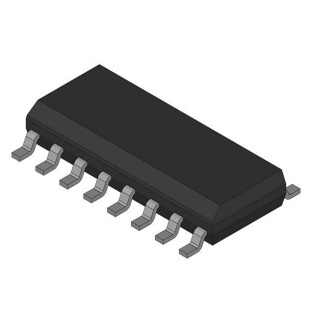
16-Pin SOIC Package
Ambient Temperature Range: −40˚C to 85˚C
Applications
n USB Root, Self-Powered, and Bus-Powered Hubs
n USB Devices such as Monitors and Printers
n General Purpose High Side Switch Applications
10125832
10125833
Functional Diagram
10125801
© 2005 National Semiconductor Corporation
DS101258
www.national.com
LM3543 Triple Port USB Power Distribution Switch and Over-Current Protection
June 2005
�LM3543
Connection Diagrams
LM3543-H
16-Pin SOIC
LM3543-L
16-Pin SOIC
10125802
10125829
Top View
Top View
Ordering Information
Part Number
Enable, Delivery Option
LM3543M-H
Active High Enable
LM3543M-L
Active Low Enable
LM3543MX-H
Active High Enable, 2500 units per reel
LM3543MX-L
Active Low Enable, 2500 units per reel
Package Type
SO-16
NS Package Number M16A
Typical Application Circuit
10125804
FIGURE 1. The LM3543 used in a Self-Powered or Root USB Hub
www.national.com
2
�Lead Temperature Range
(Soldering, 5 sec.)
If Military/Aerospace specified devices are required,
please contact the National Semiconductor Sales Office/
Distributors for availability and specifications.
Voltage at INX and OUTX pins
(Note 2)
ESD Rating (Note 3)
−0.3V to 6V
2 kV
Operating Ratings
−0.3V to 5.5V
Voltage at ENX(ENX) and FLAGX
pins
Power Dissipation
260˚C
Supply Voltage Range
Internally Limited
Maximum Junction Temperature
Storage Temperature Range
2.7V to 5.5V
Continuous Output Current Range
(Each Output)
Junction Temperature Range
150˚C
0 mA to 500 mA
−40˚C to 125˚C
−65˚C to 150˚C
DC Electrical Characteristics
Limits in standard typeface are for TJ = 25˚C, and limits in boldface type apply over the full operating temperature range. Unless otherwise specified: VIN = 5.0V, ENX = VIN (LM3543-H) or ENX = 0V (LM3543-L).
Symbol
Parameter
Typ
Max
VIN = 5V, IOUTX = 0.5A
Conditions
90
125
VIN = 3.3V, IOUTX = 0.5A
95
130
RON
On Resistance
IOUT
OUTX Continuous Output
Current
3.0V ≤ VIN ≤ 5.5V
ILEAK-OUT
OUTX Leakage Current
ENX = 0 (ENX = VIN);
TJ = 25˚C
Min
0.5
OUTX Short-Circuit Current
(Note 4)
0.01
OCTHRESH
Overcurrent Threshold
VL_FLAG
FLAGX Output-Low Voltage
OUTX Connected to GND
I(FLAGX) = 10 mA
ILEAK-FLAG
FLAGX Leakage Current
2.7 ≤ VFLAG ≤ 5.5V
ILEAK-EN
ENx Input Leakage Current
ENx/ENx = 0V or
ENx/ENx = VIN
−0.5
VIH
EN/EN Input Logic High
2.7V ≤ VIN ≤ 5.5V
2.4
VIL
EN/EN Input Logic Low
4.5V ≤ VIN ≤ 5.5V
VUVLO
Under-Voltage Lockout
Threshold
1
µA
10
µA
0.8
1.25
A
2.0
3.2
A
0.1
0.3
V
1
µA
0.5
µA
0.2
V
0.8
2.7V ≤ VIN ≤ 4.5V
IDDON
Operational Supply Current
IDDOFF
Shutdown Supply Current
mΩ
A
ENX = 0 (ENX = VIN);
− 40 ≤ TJ ≤ 85˚C
ISC
Units
V
0.4
1.8
600
µA
ENx = VIN (ENx = 0 );
−40˚C ≤ TJ ≤ 125˚C
800
µA
ENx = 0 (ENx = VIN);
TJ = 25˚C
1
µA
−40˚C ≤ TJ ≤ 125˚C
5
µA
ENx = VIN (ENx = 0 );
TJ = 25˚C
375
V
Note 1: Absolute Maximum Ratings indicate limits beyond which damage to the device may occur. Electrical specifications do not apply when operating the device
beyond its rated operating conditions.
Note 2: The maximum allowable power dissipation is a function of the Maximum Junction Temperature (TJMAX), Junction to Ambient Thermal Resistance (θJA), and
the Ambient Temperature (TA). The LM3543 in the 16-pin SOIC package has a TJMAX of 150˚C and a θJA of 130˚C/W. The maximum allowable power dissipation
at any temperature is PMAX = (TJMAX − TA)/θJA. Exceeding the maximum allowable power dissipation will cause excessive die temperature, and the part will go into
thermal shutdown.
Note 3: The Human body model is a 100 pF capacitor discharged through a 1.5 kΩ resistor into each pin.
Note 4: Thermal Shutdown will protect the device from permanent damage.
3
www.national.com
LM3543
Absolute Maximum Ratings (Note 1)
�LM3543
AC Electrical Characteristics
Limits are for TJ = 25˚C and VIN = 5.0V.
Symbol
Parameter
Conditions
Min
Typ
Max
Units
tr
OUTx Rise Time (Note 5)
CL = 33 µF, ILOAD = 500mA
1.5
ms
tf
OUTx Fall Time (Note 6)
CL = 33 µF, ILOAD = 500mA
0.9
ms
tON
Turn-on Delay (Note 7)
CL = 33 µF, ILOAD = 500mA
2.9
ms
tOFF
Turn-off Delay (Note 8)
CL = 33 µF, ILOAD = 500mA
0.7
ms
Flag Delay (Note 9)
IFLAG = 10 mA
7
ms
tF
Note 5: Time for OUTx to rise from 10% to 90% of its enabled steady-state value after ENx (ENx) is asserted.
Note 6: Time for OUTx to fall from 10% to 90% of its enabled steady-state value after ENx (ENx) is deasserted.
Note 7: Time between ENx rising through VIH (ENx falling through VIL) and OUTx rising through 90% of its enabled steady-state voltage.
Note 8: Time between ENx falling through VIL (ENx rising through VIH) and OUTx falling through 10% of its enabled steady-state voltage.
Note 9: Time between ENx rising through VIN (ENx falling through VIN) and FLAGX falling through 0.3V when OUTX is connected to GND.
Pin Descriptions
Pin Number
Pin Name
Pin Function
2, 6
IN 1, 2
Supply Inputs: These pins are the inputs to the power switches and the supply
input for the IC. In most applications they are connected together externally
and to a single input voltage supply.
1, 5
GND 1, 2
15, 14, 11
OUT 1, 2, 3
3, 4, 7
LM3543-H: EN 1, 2, 3
LM3543-L: EN 1, 2, 3
16, 13, 12
FLAG 1, 2, 3
8, 9, 10
N/C
www.national.com
Grounds: Must be connected together and to a common ground.
Switch Outputs: These pins are the outputs of the high side switches.
Enable (Inputs): Active-high (or active-low) logic enable inputs.
Fault Flag (Outputs): Active-low open drain outputs. Indicates over-current,
UVLO or thermal shutdown.
No Internal Connection.
4
�VIN = 5.0, IOUT_X = 500mA, TA = 25˚C unless otherwise speci-
RON vs Input Voltage
RON vs Junction Temperature
10125806
10125805
Quiescent Current, Output(s) Enabled vs
Junction Temperature
Quiescent Current, Output(s) Disabled vs
Junction Temperature
10125808
10125807
Quiescent Current, Output(s) Enabled vs
Input Voltage
Quiescent Current, Output(s) Disabled vs
Input Voltage
10125810
10125809
5
www.national.com
LM3543
Typical Performance Characteristics
fied.
�LM3543
Typical Performance Characteristics VIN = 5.0, IOUT_X = 500mA, TA = 25˚C unless otherwise
specified. (Continued)
Short-Circuit Output Current vs
Junction Temperature (Note 10)
Over-Current Threshold vs
Junction Temperature (Note 10)
10125813
10125814
Under-Voltage Lockout (UVLO) Threshold vs
Junction Temperature
Turn-On Delay vs Input Voltage
(CIN = 33 µF, COUT = 33 µF)
10125815
10125811
Fault Flag Delay Time vs
Junction Temperature
Turn-Off Delay vs Input Voltage
(CIN = 33 µF, COUT = 33 µF)
10125812
www.national.com
10125816
6
�Turn-On/Turn-Off Response with 47Ω/33µF Load
Turn-On/Turn-Off Response with 10Ω/33µF Load
10125818
10125819
Enable Into a Short (Note 10)
Short Connected to Enabled Device (Note 10)
10125820
10125821
Over-Current Response with Ramped Load
on OUT1 and Fixed Load on OUT2 (Note 10)
Inrush Current to Downstream Device
when LM3543 is Enabled (Note 11)
10125822
10125823
Note 10: Output is shorted to Ground through a 100 mΩ resistor.
Note 11: Load is two capacitors and one resistor in parallel to model an actual USB load condition. The first capacitor has a value of 33 µF to model the LM3543
output capacitor. The second capacitor has a value of 10 µF to model the maximum allowable input capacitance of the downstream device. The resistor is a 47Ω
resistor to model the maximum allowable input resistance of the downstream device.
7
www.national.com
LM3543
Typical Performance Characteristics VIN = 5.0, IOUT_X = 500mA, TA = 25˚C unless otherwise
specified. (Continued)
�LM3543
rapidly discharge through the part, activating current limit
circuitry. The threshold for activating current limiting is 2.0A
(typ.). Protection is achieved by momentarily opening the
MOSFET switch and then gradually turning it on. Turn-on is
halted when the current through the switch reaches the
current-limit level of 1.0A (typ.) The current is held at this
level until either the excessive load/short is removed or the
part overheats and thermal shutdown occurs (see Thermal
Shutdown section, below). The fault flag of a switch is asserted whenever the switch is current limiting.
Functional Descriptions
POWER SWITCHES
The power switches that comprise the three ports of the
LM3543 are N-Channel MOSFETs. They have a typical onstate drain-to-source resistance of 90 mΩ when the input
voltage is 5 V. When enabled, each switch will supply a 500
mA minimum current to its load. In the unlikely event that a
switch is enabled and the output voltage of that switch is
pulled above the input voltage, the bi-directional nature of
the switch results in current to flow from the output to the
input. When a switch is disabled, current flow through the
switch is prevented in both directions.
If a port on the LM3543 is enabled into a short condition, the
output current of that port will rise to the current-limit level
and hold there.
When a port is in a current-limit condition, the LM3543
senses the output voltage on that port and, if it is less than
1.0V (typ.), will reduce the output current through that port.
This operation is shown in Figure 2, below. The current
reduction, or foldback, reduces power dissipation through
the overloaded MOSFET switch. An additional advantage of
the foldback feature is the reduction of power required from
the source supply when one or more output ports are
shorted.
CHARGE PUMP AND DRIVER
The gate voltages of the high-side NFET power switches are
supplied by an internal charge-pump and driver circuit combination. The charge pump is a low-current switchedcapacitor circuit that efficiently generates voltages above the
LM3543 input supply. The charge pump output is used to
supply a transconductance amplifier driver circuit that controls the gate voltages of the power switches. Rise and fall
times on the gates are typically kept between 2 ms and 4 ms
to limit large current surges and associated electromagnetic
interference (EMI).
ENABLE (ENx or ENx)
The LM3543 comes in two versions: an active-high enable
version, LM3543-H, and an active-low enable version,
LM3543-L. In the LM3543-H, the ENx pins are active-high
logic inputs that, when asserted, turn on the associated
power supply switch(es). Power supply switches are controlled by the ENx active-low logic inputs in the LM3543-L.
With all three ports disabled on either version of the LM3543,
less than 5 µA of supply current is consumed. Both types of
enable inputs, active-high and active-low, are TTL and
CMOS logic compatible.
INPUT AND OUTPUT
The power supply to the control circuitry and the drains of the
power-switch MOSFETs are connected to the two input pins,
IN1 and IN2. These two pins are connected externally in
most standard applications. The two ground nodes GND1
and GND2 must be connected externally in all applications.
Pins OUT1, OUT2, and OUT3 are connections to the source
nodes of the power-switch MOSFETs. In a typical application
circuit, current flows through the switches from IN1 and IN2
to OUTx toward the load.
10125817
FIGURE 2. Short-Circuit Output Current (with
Foldback) vs. Output Voltage
THERMAL SHUTDOWN
The LM3543 is internally protected against excessive power
dissipation by a two-stage thermal protection circuit. If the
device temperature rises to approximately 145˚C, the thermal shutdown circuitry turns off any switch that is current
limited. Non-overloaded switches continue to function normally. If the die temperature rises above 160˚C, all switches
are turned off and all three fault flag outputs are activated.
Hysteresis ensures that a switch turned off by thermal shutdown will not be turned on again until the die temperature is
reduced to 135˚C. Shorted switches will continue to cycle off
and on, due to the rising and falling die temperature, until the
short is removed.
The thermal shutdown function is shown graphically in Figure 3 and Figure 4.
UNDERVOLTAGE LOCKOUT (UVLO)
Undervoltage Lockout (UVLO) prevents the MOSFET
switches from turning on until the input voltage exceeds a
typical value of 1.8V.
If the input voltage drops below the UVLO threshold, the
MOSFET switches are opened and fault flags are activated.
UVLO flags function only when one or more of the ports is
enabled. Due to the paired nature of the design, both FLAG1
and FLAG2 will assert if either port1 or port2 is enabled in a
UVLO condition.
CURRENT LIMIT AND FOLDBACK
The current limit circuit is designed to protect the system
supply, the LM3543 switches, and the load from potential
damage resulting from excessive currents. If a direct short
occurs on an output of the LM3543, the input capacitor(s)
www.national.com
8
�SOFT START
(Continued)
When a power switch is enabled, high levels of current will
flow instantaneously through the LM3543 to charge the large
capacitance at the output of the port. This is likely to exceed
the over-current threshold of the device, at which point the
LM3543 will enter its current-limit mode. The amount of
current used to charge the output capacitor is then set by the
current-limit circuitry. The device will exit the current-limit
mode when the current needed to continue to charge the
output capacitor is less than the LM3543 current-limit level.
FAULT FLAG
The fault flags are open-drain outputs, each capable of
sinking up to a 10 mA load current to typically 100 mV above
ground.
A parasitic diode exists between the flag pins and VIN pins.
Pulling the flag pins to voltages higher than VIN will forward
bias this diode and will cause an increase in supply current.
This diode will also clamp the voltage on the flag pins to a
diode drop above VIN.
10125825
FIGURE 3. Thermal Shutdown Characteristics when
only the First-Stage Thermal-Shutdown Mode is
Needed
The fault flag is active (pulled low) when any of the following
conditions are present: under-voltage, current-limit, or
thermal-shutdown.
The LM3543 has an internal delay in reporting fault conditions that is typically 7 ms in length. In start-up, the delay
gives the device time to charge the output capacitor(s) and
exit the current-limit mode before a flag signal is set. This
delay also prevents flag signal glitches from occurring when
brief changes in operating conditions momentarily place the
LM3543 into one of its three error conditions. If an error
condition still exists after the delay interval has elapsed, the
appropriate fault flag(s) will be asserted (pulled low) until the
error condition is removed. In most applications, the 7 ms
internal flag delay eliminates the need to extend the delay
with an external RC delay network.
Application Information
10125826
OUTPUT FILTERING
The schematic in Figure 1 showed a typical application
circuit for the LM3543. The USB specification requires 120
µF at the output of each hub. A three-port hub with 33 µF
tantalum capacitors at each port output meets the specification. These capacitors provide short-term transient current to
drive downstream devices when hot-plug events occur. Capacitors with low equivalent-series-resistance should be
used to lower the inrush current flow through the LM3543
during a hot-plug event.
The rapid change in currents seen during a hot plug event
can generate electromagnetic interference (EMI). To reduce
this effect, ferrite beads in series between the outputs of the
LM3543 and the downstream USB port are recommended.
Beads should also be placed between the ground node of
the LM3543 and the ground nodes of connected downstream ports. In order to keep voltage drop across the beads
to a minimum, wire with small DC resistance should be used
through the ferrite beads. A 0.01 µF - 0.1 µF ceramic capacitor is recommended on each downstream port directly between the Vbus and ground pins to further reduce EMI effects.
FIGURE 4. Thermal Shutdown Characteristics when
Both First-Stage and Second-Stage Thermal-Shutdown
Modes are Needed
In Figure 3, port 1 is enabled into a short. When this occurs,
the MOSFET switch of port 1 repeatedly opens and closes
as the device temperature rises and falls between 145˚C and
135˚C. In this example, the device temperature never rises
above 160˚C. The second stage thermal shutdown is not
used and port 2 remains operational.
When port 1 is enabled into a short in the example illustrated
in Figure 4, the device temperature immediately rises above
160˚C. A higher ambient temperature or a larger number of
shorted outputs can cause the junction temperature to increase, resulting in the difference in behavior between the
current example and the previous one. When the junction
temperature reaches 160˚C, all three ports are disabled (port
3 is not shown in the figure) and all three fault-flag signals
are asserted. Just prior to time index 2.5 ms, the device
temperature falls below 135˚C, all three ports activate, and
all three fault flags are removed. The short condition remains
on port 1, however. For the remainder of the example, the
device temperature cycles between 135˚C and 145˚C, causing port 1 to repeatedly turn on and off but allowing the
un-shorted ports to function normally.
POWER SUPPLY FILTERING
A sizable capacitor should be connected to the input of the
LM3543 to ensure the voltage drop on this node is less than
330 mV during a heavy-load hot-plug event. A 33 µF, 16V
9
www.national.com
LM3543
Functional Descriptions
�LM3543
Application Information
(1)
PD = RON * IDS2
Note: Equation for power dissipation neglects portion that
comes from LM3543 quiescent current because this value
will almost always be insignificant.
Using this figure, determine the junction temperature with
Equation (2).
(2)
TJ = PD * θJA + TA.
(Continued)
tantalum capacitor is recommended. The input supply
should be further bypassed with a 0.01 µF - 0.1 µF ceramic
capacitor, placed close to the device. The ceramic capacitor
reduces ringing on the supply that can occur when a short is
present at the output of a port.
EXTENDING THE FAULT FLAG DELAY
Where:
θJA = SOIC Thermal Resistance: 130˚C/W and TA = Ambient
Temperature (˚C).
While the 7 ms (typical) internal delay in reporting flag conditions is adequate for most applications, the delay can be
extended by connecting external RC filters to the FLAG pins,
as shown in Figure 5.
Compare the calculated temperature with the expected temperature used to estimate RON. If they do not reasonably
match, re-estimate RON using a more appropriate operating
temperature and repeat the calculations. Reiterate as necessary.
PCB LAYOUT CONSIDERATIONS
In order to meet the USB requirements for voltage drop,
droop and EMI, each component used in this circuit must be
evaluated for its contribution to the circuit performance.
These principles are illustrated in Figure 6. The following
PCB layout rules and guidelines are recommended
1. Place the switch as close to the USB connector as
possible. Keep all Vbus traces as short as possible and
use at least 50-mil, 1 ounce copper for all Vbus traces.
Solder plating the traces will reduce the trace resistance.
10125828
FIGURE 5. Typical Circuit for Lengthening the Internal
Flag Delay
2.
Avoid vias as much as possible. If vias are used, use
multiple vias in parallel and/or make them as large as
possible.
3. Place the output capacitor and ferrite beads as close to
the USB connector as possible.
4. If ferrite beads are used, use wires with minimum resistance and large solder pads to minimize connection
resistance.
POWER DISSIPATION AND JUNCTION TEMPERATURE
A few simple calculations will allow a designer to calculate
the approximate operating temperature of the LM3543 for a
given application. The large currents possible through the
low resistance power MOSFET combined with the high thermal resistance of the SOIC package, in relation to power
packages, make this estimate an important design step.
Begin the estimate by determining RON at the expected
operating temperature using the graphs in the Typical Performance Characteristics section of this datasheet. Next,
calculate the power dissipation through the switch with
Equation (1).
10125827
FIGURE 6. Self-Powered Hub Connections and Per-Port Voltage Drop
www.national.com
10
�ROOT AND SELF-POWERED USB HUBS
USB BUS-POWERED FUNCTIONS AND GENERAL
IN-RUSH CURRENT LIMITING APPLICATIONS
The LM3543 can be placed at the power-supply input of USB
bus-powered functions, or other similar devices, to protect
them from high in-rush currents. If the current being delivered to the device were to exceed the 2.0A over-current
threshold (typ.) of the LM3543, switches in violation would
open to protect the device from damage.
In addition to in-rush current limiting, the LM3543 can be
used in high-power bus-powered functions to keep current
levels of the function in compliance during power-up. The
USB specification requires the staged switching of power
when connecting high-power functions to the bus. When a
high-power function is initially connected to the bus, it must
not draw more than one unit supply (100mA). After a connection is detected and enumerated, and if the upstream
device is capable of supplying the required power, the highpower function may draw up to five unit loads (500mA). With
the proper control signals, the LM3543 can be used to
achieve this staged power connection. When the function is
connected to the bus, one or more of the LM3543 switches
can be closed to connect bus power only to circuitry needed
during the connection and enumeration process. If the function is to be powered fully, remaining switches on the
LM3543 can be closed to connect all blocks of the function to
the power bus. Figure 7 illustrates how the LM3543 can be
connected for use in bus powered functions.
The LM3543 has been designed primarily for use in root and
self-powered USB hubs. In this application, the switches of
the LM3543 are used to connect the power source of the hub
to the power bus used by downstream devices and to protect
the hub from dangerously excessive loads and shorts to
ground. A high-power bus-powered function, low-power buspowered function, or a bus-powered hub can be driven
through a single port of the LM3543. A schematic of a circuit
that uses the LM3543 for power-supply switching in a typical
root or self-powered hub was shown earlier in this datasheet
in Figure 1.
Voltage drop requirements of USB power supplies require
the power outputs of the root and self-powered hubs to be no
less than 4.75V. For this reason, it is recommended that a 5V
power supply with a ± 3% output voltage tolerance is used in
this application. Combining a 3% supply with a lowresistance PCB design and the low on-resistance of the
LM3543 power switches will ensure that the hub power
outputs meet the USB voltage drop specification even with a
500mA load, the maximum allowed in the USB standard.
BUS-POWERED USB HUBS
The LM3543 is capable of performing the power supply
switching functions required in Bus-Powered hubs. Use here
is very similar to the configuration used in root and selfpowered hubs. With bus-powered hubs, however, there is no
internal power supply to drive the input pins of the LM3543.
10125831
FIGURE 7. Using the LM3543 in USB Bus-Powered Functions
11
www.national.com
LM3543
Instead, the input pins should be connected to the power bus
supplied by the upstream hub.
Typical Applications
�LM3543 Triple Port USB Power Distribution Switch and Over-Current Protection
Physical Dimensions
inches (millimeters) unless otherwise noted
Order Number LM3543M-H, LM3543M-L, LM3543MX-H or LM3543MX-L
NS Package Number M16A
National does not assume any responsibility for use of any circuitry described, no circuit patent licenses are implied and National reserves
the right at any time without notice to change said circuitry and specifications.
For the most current product information visit us at www.national.com.
LIFE SUPPORT POLICY
NATIONAL’S PRODUCTS ARE NOT AUTHORIZED FOR USE AS CRITICAL COMPONENTS IN LIFE SUPPORT DEVICES OR SYSTEMS
WITHOUT THE EXPRESS WRITTEN APPROVAL OF THE PRESIDENT AND GENERAL COUNSEL OF NATIONAL SEMICONDUCTOR
CORPORATION. As used herein:
1. Life support devices or systems are devices or systems
which, (a) are intended for surgical implant into the body, or
(b) support or sustain life, and whose failure to perform when
properly used in accordance with instructions for use
provided in the labeling, can be reasonably expected to result
in a significant injury to the user.
2. A critical component is any component of a life support
device or system whose failure to perform can be reasonably
expected to cause the failure of the life support device or
system, or to affect its safety or effectiveness.
BANNED SUBSTANCE COMPLIANCE
National Semiconductor manufactures products and uses packing materials that meet the provisions of the Customer Products
Stewardship Specification (CSP-9-111C2) and the Banned Substances and Materials of Interest Specification (CSP-9-111S2) and contain
no ‘‘Banned Substances’’ as defined in CSP-9-111S2.
Leadfree products are RoHS compliant.
National Semiconductor
Americas Customer
Support Center
Email: new.feedback@nsc.com
Tel: 1-800-272-9959
www.national.com
National Semiconductor
Europe Customer Support Center
Fax: +49 (0) 180-530 85 86
Email: europe.support@nsc.com
Deutsch Tel: +49 (0) 69 9508 6208
English Tel: +44 (0) 870 24 0 2171
Français Tel: +33 (0) 1 41 91 8790
National Semiconductor
Asia Pacific Customer
Support Center
Email: ap.support@nsc.com
National Semiconductor
Japan Customer Support Center
Fax: 81-3-5639-7507
Email: jpn.feedback@nsc.com
Tel: 81-3-5639-7560
�