LM3551, LM3552
www.ti.com
SNVS371D – AUGUST 2005 – REVISED MAY 2013
LM3551 /LM3552 1A White LED Driver with Flash Timeout Protection
Check for Samples: LM3551, LM3552
FEATURES
DESCRIPTION
•
•
•
•
•
•
•
•
•
The LM3551 and LM3552 are fixed frequency,
current mode step-up DC/DC converters with two
integrated NFETs that can be used for precision LED
brightness control. The devices are capable of driving
loads up to 1A from a single-cell Li-Ion battery.
1
2
Up to 1A Total Drive Current
Flash Timeout Protection
Independent Torch/Flash/Shutdown Modes
LED Disconnect in Shutdown
Programmable Soft-Start Limits Inrush Current
Over-Voltage Protection
Wide Voltage Range 2.7 to 5.5V
1.25MHz Constant Switching Frequency
Small, Low Profile Package, Non-Pullback
WSON(4mm x 4mm)
The LM3551 and LM3552 can drive one or more high
current flash LEDs either in a high power Flash mode
or a lower power Torch mode using the
TORCH/FLASH pin. A programmable Timeout
function on the FTO pin forces the internal NFETs to
turn off after a certain user defined time. An external
SD pin (LM3551) or EN pin (LM3552) is available to
put the device into low power shutdown mode. During
shutdown, the feedback resistors and the load are
disconnected from the input to avoid leakage current
paths to ground.
APPLICATIONS
•
•
•
•
•
•
White LED Camera Flash
White LED Torch (Flashlight)
DSC (Digital Still Camera) Flash
Cellular Camera Phone Flash
PDA Camera Flash
Camcorder Torch (Flashlight) Lamp
User programmable soft-start circuitry has been
integrated to eliminate large inrush currents at startup. Over-voltage protection circuitry and a 1.25MHz
switching frequency allow for the use of small, lowcost output capacitors with lower voltage ratings. The
LM3551 and LM3552 are available in a low profile 14pin WSON package.
Typical Application Circuits
Sharp
GM5BW05340A
Flash LED
D1
L1
VBAT
+ -
RC
CC
SW
VIN
CIN
FB
VC
FTO
L1
SD/ T/F
EN
D1
SW
SS
CSS
LUMILED
LXCL-PWF1
Flash LED
OVP
+ -
FB
CIN
COUT
RC
CC
RF
FET-T
FET-F
CFTO
VIN
COUT
RT
LM3551/2
GND
VBAT
OVP
VC
FTO
RT
LM3551/2
RF
FET-T
FET-F
CFTO
SD/
EN
T/F
SS
CSS
1
2
Please be aware that an important notice concerning availability, standard warranty, and use in critical applications of
Texas Instruments semiconductor products and disclaimers thereto appears at the end of this data sheet.
All trademarks are the property of their respective owners.
PRODUCTION DATA information is current as of publication date.
Products conform to specifications per the terms of the Texas
Instruments standard warranty. Production processing does not
necessarily include testing of all parameters.
Copyright © 2005–2013, Texas Instruments Incorporated
�LM3551, LM3552
SNVS371D – AUGUST 2005 – REVISED MAY 2013
www.ti.com
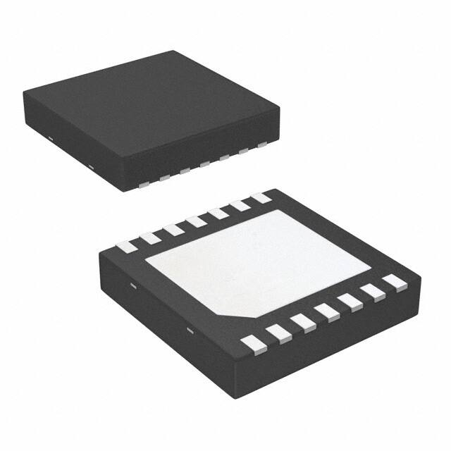
Connection Diagram
14-Pin WSON Package
1
14
14
2
13
13
12
12
4
Die-Attach
Pad(DAP)
11
5
GND
3
1
2
3
11
Die-Attach
Pad(DAP)
10
10
GND
5
6
9
9
6
7
8
8
7
Top View
4
Bottom View
Figure 1. Package Number NHL0014B
PIN DESCRIPTIONS
Pin
Name
9
VIN
Input Voltage. Input range: 2.7V to 5.5V.
Function
13
T/F
TORCH/FLASH Pin. Low = Torch Mode, High = Flash Mode
8
SW
Switch Pin
10
OVP
Over Voltage Protection Pin
3
VC
5
SD(LM3551)
EN(LM3552)
12
FTO
11
SS
Soft Start Pin
4
FB
Feedback Pin
14
FET-T
Torch FET Drain
Flash FET Drain
2
FET-F
1,7,DAP
GND
6
AGND
Compensation network connection. Connected to the output of the voltage error amplifier.
Shutdown pin logic input. High = Shutdown, Low = Enabled
Enable pin logic input. High = Enabled, Low = Shutdown
Flash Timeout. External capacitor determines max. duration allowed flash pulse
Ground
Analog Ground. Connect the ground of the compensation components, CFTO and soft start cap to
AGND. AGND must be connected to the GND pin through a low impedance connection.
These devices have limited built-in ESD protection. The leads should be shorted together or the device placed in conductive foam
during storage or handling to prevent electrostatic damage to the MOS gates.
2
Submit Documentation Feedback
Copyright © 2005–2013, Texas Instruments Incorporated
Product Folder Links: LM3551 LM3552
�LM3551, LM3552
www.ti.com
SNVS371D – AUGUST 2005 – REVISED MAY 2013
Absolute Maximum Ratings (1) (2) (3)
VIN pin: Voltage to GND
7.5V
SW pin: Voltage to GND
21V
FB pin: Voltage to GND
7V
VC pin: Voltage to GND
1.26V ± 0.3V
SD,T/F pins: Voltage to GND
7.5V
FET-T, FET-F: Voltage to GND
6V
Continuous Power Dissipation (4)
Internally Limited
Junction Temperature (TJ-MAX )
150°C
Storage Temperature Range
ESD Rating (5)
(1)
(2)
(3)
(4)
(5)
-65°C to +150
Human Body Model
2.0kV
Absolute Maximum Ratings indicate limits beyond which damage to the component may occur. Operating Ratings are conditions under
which operation of the device is specified. Operating Ratings do not imply performance limits. For performance limits and associated test
conditions, see the Electrical Characteristics tables.
All voltages are with respect to the potential at the GND pin.
If Military/Aerospace specified devices are required, please contact the Texas Instruments Sales Office/ Distributors for availability and
specifications.
Internal thermal shutdown circuitry protects the device from permanent damage. Thermal shutdown engages at TJ=140ºC (typ.) and
disengages at TJ=120ºC (typ.).
The human body model is a 100pF capacitor discharged through a 1.5kΩ resistor into each pin. (MIL-STD-883 3015.7)
Operating Ratings (1) (2)
Input Voltage Range
SW Voltage Max.
2.7V to 5.5V
(3)
20V
Junction Temperature (TJ) Range
-40°C to +110°C
Ambient Temperature (TA) Range (4)
(1)
(2)
(3)
(4)
-40°C to +85°C
Absolute Maximum Ratings indicate limits beyond which damage to the component may occur. Operating Ratings are conditions under
which operation of the device is specified. Operating Ratings do not imply performance limits. For performance limits and associated test
conditions, see the Electrical Characteristics tables.
All voltages are with respect to the potential at the GND pin.
Maximum recommended SW pin voltage when the OVP pin is grounded.
In applications where high power dissipation and/or poor package thermal resistance is present, the maximum ambient temperature may
have to be derated. Maximum ambient temperature (TA-MAX) is dependent on the maximum operating junction temperature (TJ-MAX-OP =
110ºC), the maximum power dissipation of the device in the application (PD-MAX), and the junction-to-ambient thermal resistance of the
part/package in the application (θJA), as given by the following equation: TA-MAX = TJ-MAX-OP – (θJA × PD-MAX).
Thermal Properties
Junction-to-Ambient Thermal Resistance (θJA), NHL0014B Package (1)
(1)
37.3°C/W
Junction-to-ambient thermal resistance is highly application and board-layout dependent. In applications where high maximum power
dissipation exists, special care must be paid to thermal dissipation issues in board design.
Submit Documentation Feedback
Copyright © 2005–2013, Texas Instruments Incorporated
Product Folder Links: LM3551 LM3552
3
�LM3551, LM3552
SNVS371D – AUGUST 2005 – REVISED MAY 2013
www.ti.com
Electrical Characteristics (1) (2)
Limits in standard typeface are for TJ = +25° C. Limits in boldface type apply over the full operating junction temperature
range (-40°C ≤ TJ ≤ +110°C). Unless otherwise noted, specifications apply to the LM3551 and LM3552 Typical Application
Circuit (pg. 1) with: VIN = 3.6V, V(SD) = 0V for LM3551 and V(EN) = VIN for LM3552, ILOAD = 0A (3)
Symbol
IQ
Parameter
Quiescent Current
ISD
Shutdown Current
ICL (4)
Switch Current Limit
VFB
Feedback Voltage
IFB
(6)
Typ
Max
Units
FB = VIN (Not Switching)
Conditions
Min
1.47
2.0
mA
V(SD) = VIN, LM3551
2.55
5.0
V(EN) = 0V, LM3552
0.1
2.3
VIN = 3.0V (5)
2.1
1.2285
Feedback Pin Bias Current
1.265
µA
A
1.2915
V
50
nA
135
µmho
Error Amp Voltage Gain
135
V/V
Maximum Duty Cycle
92.5
%
gm
Error Amp Transconductance
AV
DMAX
fsw
Switching Frequency
ISDPIN
Shutdown Pin Current
(LM3551)
IENPIN
Enable Pin Current
(LM3552)
IT/FPIN
T/F Pin Current
IL-SW
SW Pin Leakage Current
RDSON-SW
SW Pin RDSON
IL-T
ΔI = 5µA
0.9
1.25
1.6
MHz
VSD = 0V
3.0
6
µA
VEN = 3.6V
3.0
6
µA
VT/F = 0V
26
VT/F = VIN
22
nA
VL-SW = 20V
0.07
ISW = 0.5A
0.165
Ω
FET-T Leakage Current
0.1
µA
RDSON-T
FET-T RDSON
0.98
Ω
IL-F
FET-F Leakage Current
0.1
µA
RDSON-F
FET-F RDSON
0.36
Ω
ThSD/EN
Shutdown/Enable Pin
Threshold
ThT/F
T/F Pin Threshold
UVP
Under Voltage Protection
Thresholds
On Threshold
2.25
2.48
2.70
Off Threshold
2.43
2.58
2.77
OVP
Over Voltage Protection
Thresholds
On Threshold
11.3
12.4
14
Off Threshold
9.2
10.6
12
VFTO
Flash Timeout trip-point
0.99
1.16
1.32
V
IFTO
Flash Timeout Current
1.12
1.4
1.68
µA
VSS
Soft-Start Voltage
1.18
1.25
1.32
V
ISS
Soft-Start Current
10
11.5
13
µA
(1)
(2)
(3)
(4)
(5)
(6)
4
Output High
1.2
Output Low
Output High
8
0.3
1.2
Output Low
0.3
µA
V
V
V
V
All voltages are with respect to the potential at the GND pin.
Min and Max limits are specified by design, test, or statistical analysis. Typical (Typ) numbers represent the most likely norm. Unless
otherwise specified, conditions for Typ specifications are: VIN = 3.6V and TA = 25ºC.
CIN and COUT,: Low-ESR Surface-Mount Ceramic Capacitors (MLCCs) used in setting electrical characteristics
Duty cycle affects current limit due to ramp generator.
Current limit at 0% duty cycle. See TYPICAL PERFORMANCE section for Switch Current Limit vs. VIN
Bias current flows into FB pin.
Submit Documentation Feedback
Copyright © 2005–2013, Texas Instruments Incorporated
Product Folder Links: LM3551 LM3552
�LM3551, LM3552
www.ti.com
SNVS371D – AUGUST 2005 – REVISED MAY 2013
Typical Performance Characteristics
Unless otherwise specified: TA = +25°C; VIN = 3.6V; L = 4.7µH, (RC = 10kΩ, CC = 4.7nF, CIN = COUT = 10µF for Lumiled LED),
(RC = 27kΩ, CC = 10nF, CIN = 10µF, COUT = 4.7µF for Sharp LED), CFTO = 1µF, CSS= 0.1µF.
ICL measure when VOUT = 95% × VOUT (nominal)
Current Limit vs. Input Voltage
VOUT = 5V
Current Limit vs. Input Voltage
VOUT = 10V
Figure 2.
Figure 3.
ICL measure when VOUT = 95% × VOUT (nominal)
Converter Efficiency vs. Input Voltage
Lumiled Flash LED
Converter Efficiency vs. Input Voltage
Sharp Flash LED
Figure 4.
Figure 5.
IOUT measured at 95%× VOUT (nominal)
Maximum IOUT vs. Input Voltage
VOUT = 5V
Maximum IOUT vs. Input Voltage
VOUT = 10V
Figure 6.
Figure 7.
IOUT measured at 95%× VOUT (nominal)
Submit Documentation Feedback
Copyright © 2005–2013, Texas Instruments Incorporated
Product Folder Links: LM3551 LM3552
5
�LM3551, LM3552
SNVS371D – AUGUST 2005 – REVISED MAY 2013
www.ti.com
Typical Performance Characteristics (continued)
Unless otherwise specified: TA = +25°C; VIN = 3.6V; L = 4.7µH, (RC = 10kΩ, CC = 4.7nF, CIN = COUT = 10µF for Lumiled LED),
(RC = 27kΩ, CC = 10nF, CIN = 10µF, COUT = 4.7µF for Sharp LED), CFTO = 1µF, CSS= 0.1µF.
6
LED Torch Current
vs.
Input Voltage
Lumiled Flash LED
LED Flash Current
vs.
Input Voltage
Lumiled Flash LED
Figure 8.
Figure 9.
OVP Trip Voltage
vs.
Input Voltage
Switching Frequency
vs.
Input Voltage
Figure 10.
Figure 11.
Start-Up Waveform
Sharp LED
Start-Up Waveform
Lumiled LED
Figure 12. Ch1 = VSD, Ch3 = ILED, Ch4 = IIN
Figure 13. Ch1 = VSD, Ch3 = ILED, Ch4 = IIN
Submit Documentation Feedback
Copyright © 2005–2013, Texas Instruments Incorporated
Product Folder Links: LM3551 LM3552
�LM3551, LM3552
www.ti.com
SNVS371D – AUGUST 2005 – REVISED MAY 2013
Typical Performance Characteristics (continued)
Unless otherwise specified: TA = +25°C; VIN = 3.6V; L = 4.7µH, (RC = 10kΩ, CC = 4.7nF, CIN = COUT = 10µF for Lumiled LED),
(RC = 27kΩ, CC = 10nF, CIN = 10µF, COUT = 4.7µF for Sharp LED), CFTO = 1µF, CSS= 0.1µF.
Typical Switching Waveform
Figure 14. Sharp LED in Flash Mode
Ch1 = VSW, Ch3 = ILED, Ch4 = IL
Block Diagram
SS
Load Current
Measurement
LM3551/2
PWM COMP
FET-T
Oscillator
¦
+
-
ERROR AMP
+
-
FB
+
SD / EN
SW
Duty
Cycle
Limit
Set
Reset
Reset
Drive
LOGIC
UVP
OVP
Thermal
SD
+
-
BG
OVP COMP
Bandgap
Voltage
Reference
Thermal
Shutdown
FET-F
Shutdown
Comparator
OVP
VIN
LM3551
Flash
Timeout
T/F
LM3552
GND
VC
FTO
AGND
SD/EN
OVP
VIN
GND
Submit Documentation Feedback
Copyright © 2005–2013, Texas Instruments Incorporated
Product Folder Links: LM3551 LM3552
7
�LM3551, LM3552
SNVS371D – AUGUST 2005 – REVISED MAY 2013
www.ti.com
Circuit Description
OVERVIEW
The LM3551/2 are high power white LED flash drivers capable of delivering up to 1A of output current. The
devices utilize a highly efficient inductive DC/DC boost converter to achieve the required output voltage. A
current-mode PWM control scheme regulates the output current over a wide input voltage range. Both the
LM3551 and the LM3552 have two low-side load disconnect FET's allowing for a continuous low-power Torchmode and a high-power, short duration Flash-mode.
Several application specific safety features are integrated into the LM3551/2 design. A flash timeout circuit is
present on-chip to prevent a failure in the flash LED caused by a timing violation. Over-Voltage Protection
protects the output capacitor, inductor and main power switch in the event of an open circuit condition. Other
safety features include inductor current limit, thermal shutdown, and an undervoltage lockout.
CIRCUIT COMPONENTS
Inductive DC/DC Boost Converter
In order to achieve the output voltages required to power high power white LEDs, the LM3551 and LM3552
utilize a highly efficient inductive DC/DC converter. The boost converter utilizes a current-mode controlled,
constant frequency (1.25MHz.), PWM architecture. This architecture creates a predictable noise spectrum that
allows for easy filtering and low noise. A very low on-resistance power NFET(RDSON = 0.165Ω) and high value
current limit (2.2A typ.) help efficiently provide a high power output (700mA@5V) over the entire lithium-ion
voltage range. The feedback voltage for both the LM3551 and LM3552 is tightly regulated to 1.265V.
SD/EN Pin
The LM3551 and LM3552 provide two different options in regards to turn-on control logic. The LM3551 utilizes a
shutdown pin (SD) that turns on the part when a voltage less than 0.3V is applied. An internal 1.2MΩ pull-up to
VIN is provided to place the LM3551 into shutdown when no control signal is provided. The LM3552 utilizes a
enable pin (EN) that turns on the part when a voltage greater than 1.2V is applied. An internal 1.2MΩ pull-down
to GND is provided to place the LM3552 into shutdown when no control signal is provided.
Low-side Load Disconnect FETs
The LM3551 and LM3552 have two low-side load disconnect NFETs (FET-T and FET-F) that provide the
physical mechanism of Torch Mode and Flash Mode. In Torch Mode, FET-T is enabled allowing current to flow
through it. FET-T has an on-resistance of 0.98Ω and is capable of handling currents up to 200mA. In Flash
Mode, both FET-T and FET-F are enabled. FET-F has an on-resistance of 0.36Ω and is capable of handling
currents up to 500mA. The total Flash current is equal to the sum total of the current flowing through FET-T and
FET-F. See the CURRENT SET EQUATIONS in the Application Informations section for more information
regarding setting LED current .
In shutdown mode, the LM3551/2 provide a true load disconnect helping to keep the total shutdown current to a
minimum.
Over-Voltage Protection (OVP)
The over voltage protection (OVP) is engaged when a failure mode occurs (FB pin grounded, Flash LED
becomes open or disconnected, etc.). In the event of a failure, OVP prevents the output voltage from exceeding
12.4V (typ). When the OVP level is reached, the switch FET shuts off preventing the output voltage from climbing
higher. Once the FET has shut off, the output will droop at a rate determined by the value of the output capacitor
and current leakage through the OVP pin and any other leakage path. When the output voltage drops to
10.6V(typ), switching will resume. The LM3551 and LM3552 will go back into OVP if the failure is still present
resulting in a pulsed output condition.
NOTE
To disable OVP, ground to OVP pin. CAUTION: The LM3551 and LM3552 may be
damaged if an OVP condition occurs and OVP is disabled.
8
Submit Documentation Feedback
Copyright © 2005–2013, Texas Instruments Incorporated
Product Folder Links: LM3551 LM3552
�LM3551, LM3552
www.ti.com
SNVS371D – AUGUST 2005 – REVISED MAY 2013
Under-Voltage Protection (UVP)
Both the LM3551 and LM3552 have under-voltage protection circuitry (UVP). This protects the NMOS power
device during startup and shutdown by preventing operation at voltages less than the minimum input voltage.
The UVP protection is enabled at 2.48V(typ.) and will not disable until the input voltage rises above 2.58V(typ.) .
Torch/Flash Pin (T/F)
The TORCH/FLASH pin (T/F) controls whether the LM3551/2 is in continuous torch mode, or in flash mode. A
logic '0' places the part into torch mode and a logic '1' places the part into flash mode. There are no pull-ups or
pull-downs internally connected to T/F. When placed into torch mode, FET-T is enabled allowing the current set
by RT to flow. In torch mode, FET-F is not enabled. Flash mode enables both FET-T and FET-F allowing the sum
total of the current set by the two external resistors, RT and RF, to flow.
Flash Timeout Protection (FTP)
When SD is low(LM3551) or EN is high(LM3552), and T/F is high, a current is output to an external capacitor,
CFTO. This causes the voltage on the capacitor to rise. If the voltage reaches Vtrip (1.16V(typ)), the timeout circuit
forces the INTERNAL_EN signal to go low, which in turn shuts-off the low-side torch and flash FETs in addition
to disabling the main power SW FET. At such time, the LED will be turned off. The part will remain disabled until
SD is pulled high (LM3551) or EN is pulled low (LM3552) and/or T/F is pulled low. At that point, the part will
return to normal operating mode. The diagram below shows a first pulse which exceeds the timeout period and
internal_EN being driven low. The second FLASH pulse is shorter than the timeout period and therefore the
voltage on CFTO never reaches Vtrip. For information on component selection, please see the FLASH TIMEOUT
EQUATIONS below.
TFTO = CFTO × (ΔVFTO ÷ IFTO)
ΔVFTO = 1.16V and IFTO= 1.4µA TFTO = Desired Timeout Duration
CFTO(µF) = TFTO(sec.) × 1.21(µA/V)
(1)
(2)
(3)
To disable the timeout function, ground the FTO pin.
EXTERNAL/INTERNAL
ITO
INTERNAL EN
CFTO
FTO
SD / EN
SD / EN
EN
SD
T/F
VTRIP
T/F
VCFTO
INTERNAL EN
Figure 15. Flash Timeout Protection Diagram
Submit Documentation Feedback
Copyright © 2005–2013, Texas Instruments Incorporated
Product Folder Links: LM3551 LM3552
9
�LM3551, LM3552
SNVS371D – AUGUST 2005 – REVISED MAY 2013
www.ti.com
Soft-Start
The LM3551 and LM3552 have a soft-start pin that can be used to limit the inductor inrush current on start-up.
The external SS pin is used to tailor the soft-start for a specific application but is not required for all applications
and can be left open when not needed. When used, a current source charges the external soft-start capacitor,
CSS, forcing the internal reference to ramp-up at a user determined rate.
Table 1. Typical Start-Up TimesVIN = 3.6V, TA = +25°C
CSS (µF)
0.1
0.47
1.0
10
Load (mA)
Start-Up Time (msec.)
Sharp LED @ 75mA Torch
3
Sharp LED @ 250mA Flash
8
Lumiled LED @ 200mA Torch
1.6
Lumiled LED @ 700mA Flash
6
Sharp LED @ 75mA Torch
12
Sharp LED @ 250mA Flash
35
Lumiled LED @ 200mA Torch
6
Lumiled LED @ 700mA Flash
35
Sharp LED @ 75mA Torch
25
Sharp LED @ 250mA Flash
75
Lumiled LED @ 200mA Torch
30
Lumiled LED @ 700mA Flash
70
Submit Documentation Feedback
Copyright © 2005–2013, Texas Instruments Incorporated
Product Folder Links: LM3551 LM3552
�LM3551, LM3552
www.ti.com
SNVS371D – AUGUST 2005 – REVISED MAY 2013
APPLICATION INFORMATION
LM3551 AND LM3552 FUNCTIONALITY TRUTH TABLE
SD (LM3551)
or
EN (LM3552)
T/F
LM3551 Result
LM3552 Result
1
0
Shut-down
Torch Mode
1
1
Shut-down
Flash Mode
0
0
Torch Mode
Shut-down
0
1
Flash Mode
Shut-down
The LM3551 has a 1.2MΩ pull-up to VIN on SD and the LM3552 has a 1.2MΩ pull-down to GND on EN.
CURRENT SET EQUATIONS
The LM3551/2 utilize inline resistors to set the Torch and Flash LED currents. The Torch-Mode current
(continuous) and the Flash-Mode current (pulsed) are programmed by placing the appropriately selected
resistors between the feedback pin (FB) and FET-T (torch FET) and FET-F (flash FET) pins. Torch-mode is set
by utilizes the current through one resistor while Flash-mode is set by utilizes the currents though both current
set resistors. The following equations are used to set the LED currents.
RTORCH = (1.265V / ITORCH) - RDSON-T
RFLASH = (1.265V / (IFLASH- ITORCH)) - RDSON-F
RDSON-T= 0.98Ω and RDSON-F = 0.36Ω
(4)
(5)
(6)
NOTE
Flash LEDs from different manufacturers can have very different continuous and pulse
current ratings. See the manufacturers datasheets to ensure that the proper current levels
are used to avoid damaging the flash LED.
INDUCTOR SELECTION
Special care must be taken when selecting an inductor for use in LM3551/2 applications. The inductor should
have a current saturation rating that is larger than the worst case peak inductor current of the application to
ensure proper operation. Using an inductor with a lower saturation current rating than is required can cause a
dramatic drop in the inductance and can derate the maximum output current levels severely. It is worth noting
that the output voltage ripple is also affected by the total ripple current in the inductor. The following equations
can help give a good approximation as to what the peak inductor current will be for a given application at room
temperature (TA = +25°C).
IL(average) = [ILED × VOUT-MAX] ÷ [VIN-MIN × Eff.]
ΔIL = [VIN × D] ÷ [L × FSW]
IL(peak) = IL(ave) + [ΔIL ÷ 2]
(7)
(8)
(9)
VOUT-MAX Maximum Output Voltage. Maximum output voltage over temperature with OVP used is 11V (12.4V
typically).
VIN-MIN Minimum Input Voltage. Recommended minimum input voltage is 3.0V. The LM3551/2 will work down to
2.7V however, use at lower input voltages will required an inductor with a higher saturation current rating.
Eff.
Converter Efficiency (approx. 85% over input voltage range).
D
Duty Cycle = 1 - [VIN / VOUT]
L
Inductance. Recommended inductance value is 4.7µH.
FSW
Switching Frequency = 1.25MHz
Submit Documentation Feedback
Copyright © 2005–2013, Texas Instruments Incorporated
Product Folder Links: LM3551 LM3552
11
�LM3551, LM3552
SNVS371D – AUGUST 2005 – REVISED MAY 2013
www.ti.com
DIODE SELECTION
The output diode for a boost regulator must be chosen correctly depending on the output voltage and output
current. The output diode must have a reverse voltage rating equal to or greater than the output voltage used.
The average current rating must be greater than the maximum load current expected, and the peak current rating
must be greater than the peak inductor current. Using Schottky diodes with lower forward voltage drop will
decrease power dissipation and increase efficiency.
CAPACITOR SELECTION
Input Capacitor
An input capacitor is required to reduce the input ripple and noise for proper operation of the regulator. The size
used is dependant on the application and board layout. If the regulator will be loaded uniformly, with very little
load changes, and at lower current outputs, the input capacitor size can often be reduced. The size can also be
reduced if the input of the regulator is very close to the source output. The size will generally need to be larger
for applications where the regulator is supplying nearly the maximum rated output or if large load steps are
expected. A minimum value of 10µF should be used under normal operating condtions while a 10-22µF capacitor
may be required for higher power and dynamic loads. Larger values and/or lower ESR may be needed if the
application requires very low ripple on the input source voltage.
Output Capacitor
A minimum output capacitor value of 4.7µF (Sharp LED) and 10µF (Lumiled) is recommended and may be
increased to a larger value. The ESR of the output capacitor is important because it determines the peak to peak
output voltage ripple according to the approximate equation:
ΔVOUT ≊ 2 × ΔIL× RESR (in Volts)
(10)
After choosing the output capacitor you can determine a pole-zero pair introduced into the control loop by the
following equations:
fP1 =
1
2S>RESR + (VOUT/ILED)]COUT
fZ1 =
Hz
1
Hz
2SRESRCOUT
(11)
The zero created by the ESR of the output capacitor is generally at a very high frequency if the ESR is small. If
low ESR capacitors are used it can be neglected. The output capacitor pole information is useful in selecting the
proper compensation components and is discussed in the Compensation Components section of the datasheet.
Capacitor Properties
Surface-mount multi-layer ceramic capacitors are recommended for both the input and output capacitors. These
capacitors are small, inexpensive and have very low equivalent series resistance (ESR