LM3553
www.ti.com
SNVS414B – FEBRUARY 2008 – REVISED MAY 2013
LM3553 1.2A Dual Flash LED Driver System with I2C Compatible Interface
Check for Samples: LM3553
FEATURES
1
•
2
•
•
•
•
•
•
•
•
•
•
•
•
Accurate and Programmable LED Current up
to 1.2A in 128 Steps
Total Solution Size < 30mm2
90% Peak Efficiency
Drives 2 LEDs in Series with 1.2A from 5V
Input
Drives 2 LEDs in Series with 600mA from 3.0V
Input
Drives 1 LED with 1.2A from 3.0V Input
Adjustable Over-Voltage Protection Allows for
Single or Series LED Operation
Four Operating Modes: Torch, Flash, Indicator,
and Voltage Mode (4.98V)
Programmable Flash Pulse Safety Timer in 16
Steps
TX Input Ensures Synchronization with RF
Power Amplifier Pulse or Prevents LED from
Overheating
LED Disconnect During Shutdown
Flash/Imager Synchronization via FEN Pin
Active Low Hardware Reset
•
•
Multi-Function Pin (RESET and GPIO)
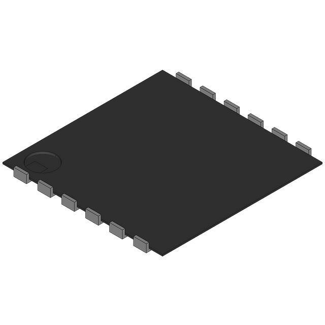
Low Profile 12-pin WSON Package
(DQB0012A: 3mm x 3mm x 0.8mm, 0.4mm
pitch)
APPLICATIONS
•
•
•
Camera Phone LED Flash
Smartphone and PDA Flash
LED Backlight
DESCRIPTION
The LM3553 is a fixed frequency, current mode stepup DC/DC converter with two regulated current sinks.
The device is capable of driving loads up to 1.2A
from a single-cell Li-Ion battery.
The LM3553 includes a TX pin that forces Torch
mode during a flash event allowing for
synchronization between the RF power amplifier and
Flash/Torch modes. It also includes a multi-function
pin (M/F) that can serve as a GPIO and a hardware
RESET pin.
The LM3553 is available in a 3mm by 3mm package.
Typical Application Circuits
2.2 PH
COUT
4.7 PF
SW
OVP
600 mA Flash
Current
COUT
D1
2.5
2.25
L
9.0
D1
-
D2
FEN
IC
9.0
1.28
+
VIN
CIN
10 PF
LM3553
TX
M/F
RSET
CIN
0.5
2
ISET
GND SCL SDA
RSET
VIO
29.25mm with 0.4mm spacing
around large components (IC and L)
Components:
L = Toko FDSE0312-2R2M
CIN = Murata GRM188R60J106ME47D
COUT = Murata GRM21BR61E475KA12L
LEDs = Lumileds LXCL ± PWF3
Or equivalent
Figure 1.
Figure 2. Solution Size
1
2
Please be aware that an important notice concerning availability, standard warranty, and use in critical applications of
Texas Instruments semiconductor products and disclaimers thereto appears at the end of this data sheet.
All trademarks are the property of their respective owners.
PRODUCTION DATA information is current as of publication date.
Products conform to specifications per the terms of the Texas
Instruments standard warranty. Production processing does not
necessarily include testing of all parameters.
Copyright © 2008–2013, Texas Instruments Incorporated
�LM3553
SNVS414B – FEBRUARY 2008 – REVISED MAY 2013
www.ti.com
Connection Diagram
12 Pin 3mm x 3mm WSON Package
DQB0012A
1
12
12
2
11
11
10
10
9
9
5
8
8
5
6
7
7
6
3
Die-Attach
Pad (DAP)
4
GND
1
Die-Attach
Pad (DAP)
GND
2
3
4
Bottom View
Top View
PIN DESCRIPTIONS
Pin
Name
Function
4
VIN
Input Voltage. Input range: 2.7V to 5.5V.
5
SW
Switch Pin
6
OVP
Over Voltage Protection Pin
2, 11
D1, D2
DAP
GND
Ground
1
ISET
Current sense input. Connect a 1% 16.5kΩ resistor to ground to set the full scale LED current.
3
FEN
Flash enable pin.
Regulated current sink inputs
8
SCL
Serial clock pin.
10
SDA
Serial data I/O pin.
9
VIO
Digital Reference Voltage level input pin.
7
TX
RF PA synchronization control pin. High = Forced Torch mode.
12
M/F
Hardware RESET or General purpose I/O. Function set through Multi-Function Control Register
These devices have limited built-in ESD protection. The leads should be shorted together or the device placed in conductive foam
during storage or handling to prevent electrostatic damage to the MOS gates.
Absolute Maximum Ratings
(1) (2) (3)
VIN pin: Voltage to GND
-0.3V to 6V
SW, OVP pin: Voltage to GND
-0.3V to 25V
D1, D2 pins: Voltage to GND
-0.3V to 25V
VIO, SCL, SDA
-0.3V to 6V
TX, FEN, M/F
Continuous Power Dissipation
-0.3V to 6V
(4)
Internally Limited
Junction Temperature (TJ-MAX )
150°C
Storage Temperature Range
-65°C to +150
(5)
Maximum Lead Temperature (Soldering)
(6)
ESD Rating
Human Body Model
(1)
(2)
(3)
(4)
(5)
(6)
2
2.5kV
Absolute Maximum Ratings indicate limits beyond which damage to the component may occur. Operating Ratings are conditions under
which operation of the device is specified. Operating Ratings do not imply performance limits. For performance limits and associated test
conditions, see the Electrical Characteristics tables.
All voltages are with respect to the potential at the GND pin.
If Military/Aerospace specified devices are required, please contact the Texas Instruments Sales Office/ Distributors for availability and
specifications.
Internal thermal shutdown circuitry protects the device from permanent damage. Thermal shutdown engages at TJ=140ºC (typ.) and
disengages at TJ=120ºC (typ.).
For detailed soldering specifications and information, please refer to Texas Instruments Application Note: AN-1187 SNOA401 for
Recommended Soldering Profiles.
The human body model is a 100pF capacitor discharged through a 1.5kΩ resistor into each pin. (MIL-STD-883 3015.7)
Submit Documentation Feedback
Copyright © 2008–2013, Texas Instruments Incorporated
Product Folder Links: LM3553
�LM3553
www.ti.com
Operating Ratings
SNVS414B – FEBRUARY 2008 – REVISED MAY 2013
(1) (2)
Input Voltage Range
2.7V to 5.5V
Junction Temperature (TJ) Range
Ambient Temperature (TA) Range
(1)
(2)
(3)
-30°C to +125°C
(3)
-30°C to +85°C
Absolute Maximum Ratings indicate limits beyond which damage to the component may occur. Operating Ratings are conditions under
which operation of the device is specified. Operating Ratings do not imply performance limits. For performance limits and associated test
conditions, see the Electrical Characteristics tables.
All voltages are with respect to the potential at the GND pin.
In applications where high power dissipation and/or poor package thermal resistance is present, the maximum ambient temperature may
have to be derated. Maximum ambient temperature (TA-MAX) is dependent on the maximum operating junction temperature (TJ-MAX-OP =
125ºC), the maximum power dissipation of the device in the application (PD-MAX), and the junction-to-ambient thermal resistance of the
part/package in the application (θJA), as given by the following equation: TA-MAX = TJ-MAX-OP – (θJA × PD-MAX).
Thermal Properties
Junction-to-Ambient Thermal Resistance (θJA), DQB0012A Package (1)
(1)
36.7°C/W
Junction-to-ambient thermal resistance is highly application and board-layout dependent. In applications where high maximum power
dissipation exists, special care must be paid to thermal dissipation issues in board design.
Submit Documentation Feedback
Copyright © 2008–2013, Texas Instruments Incorporated
Product Folder Links: LM3553
3
�LM3553
SNVS414B – FEBRUARY 2008 – REVISED MAY 2013
www.ti.com
Electrical Characteristics
Limits in standard typeface are for TA = +25°C. Limits in boldface type apply over the full operating junction temperature range
(-30°C ≤ TJ ≤ +125°C). Unless otherwise noted: VIN = 3.6V, RSET = 16.5kΩ, VD1 = VD2 = 500mV, VFB bit = '0', FEN = '0', TX =
'0', Flash Current Level = Full-Scale. (1) (2) (3)
Symbol
ILED-SUM
Parameter
Flash LED Current:
ID1+ ID2
Conditions
Flash Mode
VDX = Regulation Voltage
Min
Typ
Max
930
1020
1110
mA
Flash Mode
VDX = Regulation Voltage
RSET = 13.7kΩ
ILED-IND
Indicator Current Level
Indicator Mode
VMREG
Output Voltage Regulation in
Voltage Mode
VM = '1', EN1 = EN0 = '0'
No Load
IQ
Quiescent Supply Current
ISD
Units
1200
20
4.65
mA
4.98
5.30
V
VD1,D2 = 0V
(Switching)
1.0
1.2
mA
Shutdown Supply Current
Device Disabled
3.8
6.0
µA
IDx / ISET
LED Current to Set Current
Ratio
IDx= 500mA
VSET
ISET Pin Voltage
VD1,D2
Current Sink Regulation
Voltage
VFB Bit = '0'
450
VFB Bit = '1'
350
IDx-MATCH
Current Sink Matching
VDX = Regulation Voltage
RDSON
NMOS Switch Resistance
6770
A/A
1.24
V
mV
2
%
Ω
0.25
OCL Bit = '0'
2.2
2.5
2.8
OCL Bit = '1'
1.53
1.70
1.87
ICL
NMOS Switch Current Limit
IL-SW
SW Pin Leakage Current
Switch Off, VSW=3.6V, OVP
Mode = '0'
10
nA
IL-Dx
D1, D2 Pin Leakage
VDx = 3.5V
10
nA
VOVP
Output Over-Voltage
Protection Trip Point
OVP Mode = '1'
18.00
18.90
19.65
OVP Mode = '0'
5.4
5.6
5.85
Over-Voltage Protection
Hysteresis
OVP to Normal Operation
OVP Mode = '1'
1.6
OVPHyst
OVP Mode = '0'
0.6
IL-OVP
OVP Pin Leakage Current
VOVP=3.6V
fSW
Switching Frequency
tFD-MIN
Minimum Flash Duration Step
12.8
µsec.
DMAX
Maximum Duty Cycle
92
%
DMIN
Minimum Duty Cycle
6
ThTX,F-EN
TX, FEN Pin Threshold
1.2
tFD-MIN = 16 ÷ fSW
V
V
10
1.0
A
nA
1.35
MHz
%
On
1.0
VIN
Off
0
0.6
Input Logic High "1"
0.94
VIN
Input Logic Low "0"
0
0.64
V
Multi-Function Pin (M/F) Voltage Specifications
VM/F
Multi-Function Pin Threshold
Voltages
VOL
Output Logic Low "0"
ILOAD = 4.2mA,
GPIO Mode
V
400
mV
I2C Compatible Voltage Specifications (SCL, SDIO, VIO)
VIO
Serial Bus Voltage Level
1.45
VIN
V
VIL
Input Logic Low "0"
VIO = 3.0V
0
0.38 ×VIO
V
VIH
Input Logic High "1"
VIO = 3.0V
0.55 × VIO
VIO
V
VOL
Output Logic Low "0"
ILOAD = 3.7mA
400
mV
(1)
(2)
(3)
4
All voltages are with respect to the potential at the GND pin.
Min and Max limits are specified by design, test, or statistical analysis. Typical (Typ) numbers represent the most likely norm. Unless
otherwise specified, conditions for Typ specifications are: VIN = 3.6V and TA = 25ºC.
All testing for the LM3553 is done open-loop.
Submit Documentation Feedback
Copyright © 2008–2013, Texas Instruments Incorporated
Product Folder Links: LM3553
�LM3553
www.ti.com
SNVS414B – FEBRUARY 2008 – REVISED MAY 2013
Electrical Characteristics (continued)
Limits in standard typeface are for TA = +25°C. Limits in boldface type apply over the full operating junction temperature range
(-30°C ≤ TJ ≤ +125°C). Unless otherwise noted: VIN = 3.6V, RSET = 16.5kΩ, VD1 = VD2 = 500mV, VFB bit = '0', FEN = '0', TX =
'0', Flash Current Level = Full-Scale. (1)(2)(3)
Symbol
Parameter
Conditions
Min
Typ
Max
Units
I2C Compatible Interface Timing Specifications (SCL, SDIO, VIO)
t1
SCL (Clock Period)
2.5
µs
t2
Data In Setup Time to SCL
High
100
ns
t3
Data Out stable After SCL Low
0
ns
t4
SDA Low Setup Time to SCL
Low (Start)
100
ns
t5
SDA High Hold Time After
SCL High (Stop)
100
ns
Submit Documentation Feedback
Copyright © 2008–2013, Texas Instruments Incorporated
Product Folder Links: LM3553
5
�LM3553
SNVS414B – FEBRUARY 2008 – REVISED MAY 2013
www.ti.com
Typical Performance Characteristics
Unless otherwise specified: TA = 25°C; VIN = 3.6V; VM/F = VIN; RSET = 16.5kΩ; CIN= 10µF, COUT = 10µF;L = 2.2µH; VFB bit =
CL bit = '0'; OVP bit = '0' for 1 LED and VFB = '1' for two series LEDs;.
Maximum LED Drive Current @ VIN = 3.6V
1.6
1.2A Flash Line Regulation
1.4
TA = -30°C and +25°C
VLED = 3.65V @ +25°C
TA = +25°C
1.3
TA = +85°C
ILED (A)
ILED (A)
1.2
0.8
1.2
0.4
TA = -30°C
1.1
TA = +85°C
VLED = 3.5V @1.2A
0.0
0
32
64
96
1.0
3.0
128
3.5
4.0
Figure 3.
5.0
5.5
Figure 4.
1.0A Flash Line Regulation
Voltage Mode Line Regulation
1.1
5.250
TA = +25°C
IOUT = 500 mA
5.125
VOUT (V)
1.1
ILED (A)
4.5
VIN (V)
BRIGHTNESS CODE (#)
1.0
TA = +85°C
5.000
TA = -30°C
TA = +85°C
4.875
TA = -30°C
VLED = 3.7V @ +25°C
0.9
3.0
3.5
4.0
4.5
5.0
4.750
2.7
5.5
3.1
3.5
3.9
VIN (V)
4.7
5.1
5.5
Figure 5.
Figure 6.
Voltage Mode Load Regulation
Input Current and LED Efficiency
with 1A Flash Current
90
2.40
VLED = 3.7V and ILED = 1A
TA = +25°
IOUT = 100 mA
2.00
5.25
IIN (A)
IOUT = 500 mA
5.00
4.75
äLED
IIN
I OUT = 300 mA
VOUT (V)
4.3
VIN (V)
5.50
4.50
2.7
TA = +25°C
80
1.60
70
1.20
60
äLED (%)
1.0
IOUT = 700 mA
0.80
2.9
3.1
3.5
3.9
4.3
4.7
5.1
3.4
3.9
4.5
5.0
50
5.5
5.5
VIN (V)
VIN (V)
Figure 7.
6
Figure 8.
Submit Documentation Feedback
Copyright © 2008–2013, Texas Instruments Incorporated
Product Folder Links: LM3553
�LM3553
www.ti.com
SNVS414B – FEBRUARY 2008 – REVISED MAY 2013
Typical Performance Characteristics (continued)
Unless otherwise specified: TA = 25°C; VIN = 3.6V; VM/F = VIN; RSET = 16.5kΩ; CIN= 10µF, COUT = 10µF;L = 2.2µH; VFB bit =
CL bit = '0'; OVP bit = '0' for 1 LED and VFB = '1' for two series LEDs;.
Input Current and LED Efficiency
with 1.2A Flash Current
2.80
Input Current and LED Efficiency
with 500mA Flash Current through 2 Series LEDs
90
1.60
80
1.35
90
VLED = 3.8V and ILED = 1.2A
äLED
80
äLED
IIN (A)
äLED (%)
IIN (A)
70
70
1.10
IIN
äLED (%)
IIN
2.20
1.60
60
60
0.85
2 LEDs in Series
1.00
3.0
3.5
4.0
4.5
5.0
50
5.5
0.60
3.0
VLED = 3.35V and ILED = 500 mA
3.5
4.0
VIN (V)
4.5
5.0
50
5.5
VIN (V)
Figure 9.
Figure 10.
Input Current and LED Efficiency
with 600mA Flash Current through 2 Series LEDs
Input Current
vs
VIN
1 LED @ 1.2A and 2 LEDs @ 600mA
2.20
90
1.85
80
2.8
2.4
2.0
IIN (A)
IIN (A)
70
1.50
äLED (%)
1 LED @ 1.2A
äLED
IIN
2 LEDs @ 600 mA
1.6
60
1.15
1.2
2 LEDs in Series
VLED = 3.4V and ILED = 600 mA
0.80
3.0
3.5
4.0
4.5
5.0
50
5.5
0.8
2.7
3.1
3.5
3.9
VIN (V)
4.3
4.7
5.1
5.5
VIN (V)
Figure 11.
Figure 12.
LED Efficiency
vs
VIN
1 LED @ 1.2A and 2 LEDs @ 600mA
Converter Efficiency
vs
VIN
100
100
Voltage Mode with IOUT = 500 mA
2 LEDs @ 600 mA
ηCONVERT ER (%)
90
äLED (%)
80
1 LED @ 1.2A
60
80
2 LEDs @ 500 mA with
VLED(total) = 6.725V
70
60
1 LED @ 1A with VLED = 3.7V
50
40
2.7
3.1
3.5
3.9
4.3
4.7
5.1
40
5.5
2.7
3.1
3.5
3.9
4.3
4.7
5.1
5.5
VIN (V)
VIN (V)
Figure 13.
Figure 14.
Submit Documentation Feedback
Copyright © 2008–2013, Texas Instruments Incorporated
Product Folder Links: LM3553
7
�LM3553
SNVS414B – FEBRUARY 2008 – REVISED MAY 2013
www.ti.com
BLOCK DIAGRAM
OVP
SW
SW
Driver
OVP
SWITCH
CONTROLLER
THERMAL
SHUTDOWN
OSC
VREF
CURRENT
LIMIT
+
-
VIN
RAMP
gm
LM3553
¦
RESET/GPIO
M/F
+
RZ
0.35V or
0.450V
MIN. Dx
VOLTAGE
SELECT
CC
VIO
SDA
D2
ISTEP CTRL
2
SCL
D1
TORCH CTRL
I C INTERFACE/
CONTROL LOGIC/
REGISTERS
Tx
FLASH CTRL
Current
Control
TIME-OUT CTRL
FEN
GND
D1
Current
Sink
D2
Current
Sink
RSET
Circuit Description
CIRCUIT COMPONENTS
FEN Pin
The flash enable pin, FEN, provides an external method (non-I2C) for starting the flash pulse. When FEN is pulled
high, logic '1', the flash current level defined through the I2C interface, will be delived to the Flash LED. If the FEN
pin is driven low during the flash pulse, the flash event will stop. In the event that FEN is not pulled low during the
flash pulse, the LM3553 will continue to deliver the flash current until the safety timer duration (set through the
I2C interface) is reached.
The LM3553 does not provide a fixed off-time after the flash pulse has ended. Most flash LED manufacturers
require that the flash pulse duration be 10% of the total Flash cycle. Example: If the flash pulse duration is set to
be 200 milliseconds (Flash Duration Code= 0011), the recommended off time for the LED would be 1.8 seconds.
Please consult the LED manufacturers datasheet for exact timing requirements.
If the LM3553 is placed in indicator mode or torch mode through the I2C interface and the FEN pin is pulled high
and then low, at the end of the flash event, the LM3553 will return to the mode stored in the General Purpose
Register.
It is recommended that an external pull-down be placed between the FEN pin and GND to prevent unwanted LED
flashing during system start-up due to unknown control logic states.
8
Submit Documentation Feedback
Copyright © 2008–2013, Texas Instruments Incorporated
Product Folder Links: LM3553
�LM3553
www.ti.com
SNVS414B – FEBRUARY 2008 – REVISED MAY 2013
TX Pin
The transmission pin (TX) can be used to limit the current drawn from the battery during a PA transmission.
When the TX pin is driven high (logic '1') during a flash pulse, the LM3553 will switch to the programmed torch
current level. Once the TX pin is driven low (logic '0'), the LM3553 will return to the flash current if this event
occurs within the original flash duration.
It is recommended that an external pull-down be placed between the TX pin and GND to prevent unwanted LED
flashing during system start-up due to unknown control logic states.
M/F Pin
The multi-function pin (M/F) can be configured to provide hardware RESET or a general purpose input/output
(GPIO). All functionality is programmed through the I2C compatible interface and set in the M/F pin functionality
control register (address 0x20). The default function is a RESET, where a logic '1' places the part in the normal
operating mode, and a logic '0' places the part into a RESET state. A reset condition will place all LM3553
registers into their default states.
Connection Diagram
TX PA
Tx
SDA
LM3553
PP/PC
SCL
FEN
Imager
Figure 15. Typical System Configuration
I2C Compatible Interface
DATA VALIDITY
The data on SDA line must be stable during the HIGH period of the clock signal (SCL). In other words, the state
of the data line can only be changed when CLK is LOW.
SCL
SDA
data
change
allowed
data
valid
data
change
allowed
data
valid
data
change
allowed
Figure 16. Data Validity Diagram
A pull-up resistor between VIO and SDA must be greater than [(VIO-VOL) / 3.7mA] to meet the VOL requirement
on SDA. Using a larger pull-up resistor results in lower switching current with slower edges, while using a smaller
pull-up results in higher switching currents with faster edges.
Submit Documentation Feedback
Copyright © 2008–2013, Texas Instruments Incorporated
Product Folder Links: LM3553
9
�LM3553
SNVS414B – FEBRUARY 2008 – REVISED MAY 2013
www.ti.com
START AND STOP CONDITIONS
START and STOP conditions classify the beginning and the end of the I2C session. A START condition is
defined as SDA signal transitioning from HIGH to LOW while SCL line is HIGH. A STOP condition is defined as
the SDA transitioning from LOW to HIGH while SCL is HIGH. The I2C master always generates START and
STOP conditions. The I2C bus is considered to be busy after a START condition and free after a STOP condition.
During data transmission, the I2C master can generate repeated START conditions. First START and repeated
START conditions are equivalent, function-wise. The data on SDA line must be stable during the HIGH period of
the clock signal (SCL). In other words, the state of the data line can only be changed when CLK is LOW.
SDA
SCL
S
P
START condition
STOP condition
Figure 17. Start and Stop Conditions
TRANSFERRING DATA
Every byte put on the SDA line must be eight bits long, with the most significant bit (MSB) being transferred first.
Each byte of data has to be followed by an acknowledge bit. The acknowledge related clock pulse is generated
by the master. The master releases the SDA line (HIGH) during the acknowledge clock pulse. The LM3553 pulls
down the SDA line during the 9th clock pulse, signifying an acknowledge. The LM3553 generates an
acknowledge after each byte has been received.
After the START condition, the I2C master sends a chip address. This address is seven bits long followed by an
eighth bit which is a data direction bit (R/W). The LM3553 address is 53h. For the eighth bit, a “0” indicates a
WRITE and a “1” indicates a READ. The second byte selects the register to which the data will be written. The
third byte contains data to write to the selected register.
ack from slave
ack from slave
start
msb Chip Address lsb
w
ack
msb Register Add lsb
ack
start
Id = 53h
w
ack
addr = 10h
ack
msb
ack from slave
DATA
lsb
ack
stop
ack
stop
SCL
SDA
data = 08h
w = write (SDA = "0")
ack = acknowledge (SDA pulled down by the slave)
id = chip address, 53h for LM3553
Figure 18. Write Cycle
I2C COMPATIBLE CHIP ADDRESS
The chip address for LM3553 is 1010011, or 53hex.
10
Submit Documentation Feedback
Copyright © 2008–2013, Texas Instruments Incorporated
Product Folder Links: LM3553
�LM3553
www.ti.com
SNVS414B – FEBRUARY 2008 – REVISED MAY 2013
MSB
LSB
ADR6
bit7
ADR5
bit6
ADR4
bit5
ADR3
bit4
ADR2
bit3
ADR1
bit2
ADR0
bit1
1
0
1
0
0
1
1
R/W
bit0
2
I C Slave Address (chip address)
INTERNAL REGISTERS OF LM3553
Register
Internal Hex Address
Power On Value
General Purpose Register
0x10
0001 1000
Multi-Function Pin Control Register
0x20
1110 0000
Current Step Time Register
0x50
1111 1100
Torch Current Control Register
0xA0
1000 0000
Flash Current Control Register
0xB0
1000 0000
Flash Duration Control Register
0xC0
1111 0000
General Purpose Register
General Purpose Control
Register Address: 0x10
MSB
0
bit7
0
bit6
VFB
bit5
1
bit4
1
bit3
LSB
VM
bit2
EN1
bit1
EN0
bit0
EN0-EN1: Set Flash LED mode
Indicator Mode sets ILED = 20mA. In this mode, D1 is enabled and D2 is disabled.
VM: Enables Voltage Mode. Current sinks D1 and D2 are turned off and the LM3553 will operate in a regulated
voltage boost mode. Setting the VM bit to a '1' does not override the EN0 and EN1 bits stored in the general
purpose register. The default setting is '0'. If the LM3553 is in Voltage Mode and an indicator, torch or flash
command is issued, the LM3553 will turn on the D1 and D2 current sources and begin regulating the output
voltage to a value equal to VFB (350mV or 450mV) + VLED.
VM
EN1
EN0
Function
0
0
0
Shutdown
0
0
1
Indicator Mode
0
1
0
Torch Mode
0
1
1
Flash Mode
1
0
0
Voltage Mode
1
0
1
Indicator Mode
1
1
0
Torch Mode
1
1
1
Flash Mode
Submit Documentation Feedback
Copyright © 2008–2013, Texas Instruments Incorporated
Product Folder Links: LM3553
11
�LM3553
SNVS414B – FEBRUARY 2008 – REVISED MAY 2013
www.ti.com
VFB: Selects the regulation voltage for the LM3553. Setting this VFB bit to a '0' sets the regulation voltage to
450mV while setting the VFB bit to a '1' sets the regulation voltage to 350mV. Setting the VFB bit to a '1' during
torch mode and/or lower current flash modes (ILED < 1A) will help improve the LED efficiency of the LM3553.
M/F Pin Control Register
Multi-Function Pin Control/Options
Register Address: 0x20
MSB
1
bit7
1
bit6
1
bit5
OCL
bit4
OVP
bit3
DATA
bit2
LSB
MODE
bit1
RESET
bit0
RESET: Enables M/F as hardware RESET. '0' = Hardware RESET, .'1' = GPIO or current sink depending on the
MODE bit. Default = '0'
MODE: Sets M/F mode. Default for M0DE = '0'. '0' = GPI, and'1' = GPO
NOTE
When M/F is configured as an input, data is transfered from GPI to DATA whenever an
I2C write command is issued to the LM3553. When configuring M/F as a GPO, the first
write needs to take the LM3553 out of RESET mode and a second write can then set the
pin to the GPO.
DATA: GPIO Data. When the M/F is configured as an output (GPO), DATA sets the GPO level. Example: DATA
= '1', M/F is set high or logic '1'. When the M/F pin is configured as an input (GPI), DATA stores the GPI level.
Example: M/F = '1', DATA will be set to a '1'. Default for DATA = '0'.
OVP: Enables high-voltage OVP (OVP Bit ='1') or low-voltage OVP (OVP Bit ='0'). Default = low-voltage mode '0'
OCL: SW Pin Current Limit Selector Bit: If OCL = '0', the inductor current limit is 2.5A typ. If OCL = '1', the
inductor current limit is 1.7A typ.
Table 1. M/F Functionality Configuration Table
RESET
MODE
M/F Function
0
X
RESET
1
0
GPI
1
1
GPO
Current Step Time Register
Current Step Time
Register Address: 0x50
MSB
1
bit7
1
bit6
1
bit5
1
bit4
1
bit3
LSB
1
bit2
ST1
bit1
ST0
bit0
ST1-ST0: Sets current level stepping time for D1 and D2 during the beginning and end of the flash or torch
current waveform. '00' = 25µs, '01' = 50µs, '10' = 100µs, '11' = 200µs.
The current ramp-up/ramp-down times can be approximated by the following equation:
TRAMPUP/RAMPDOWN = (NFLASH - NSTART + 1) × tSTEP
where
•
•
N is equal to the decimal value of the brightness level
(0 ≤ NFLASH ≤ 127 and 0 ≤ NSTART ≤ 31)
NSTART = NTORCH if Torch is enabled before going into a flash. If going straight into a flash from an off-state,
NSTART = 0.
12
Submit Documentation Feedback
Copyright © 2008–2013, Texas Instruments Incorporated
Product Folder Links: LM3553
�LM3553
www.ti.com
SNVS414B – FEBRUARY 2008 – REVISED MAY 2013
Torch Current Control Register
TORCH Current Control
Register Address: 0xA0
MSB
1
bit7
0
bit6
0
bit5
TC4
bit4
TC3
bit3
LSB
TC2
bit2
TC1
bit1
TC0
bit0
TC6-TC0: Sets Torch current level for D1 and D2. xxx1 1111 = Fullscale
Flash Current Control Register
FLASH Current Control
Register Address: 0xB0
MSB
1
bit7
FC6
bit6
FC5
bit5
FC4
bit4
FC3
bit3
LSB
FC2
bit2
FC1
bit1
FC0
bit0
FC6-FC0: Sets Flash current level for D1 and D2. x111 1111 = Fullscale
Current Level Equation
The Full-Scale Flash Current Level is set through the use of an external resistor (RSET) connected to the ISET pin.
The RSET selection equation can be used to set the current through each of the two current sinks, D1 and D2.
RSET = 6770 × 1.24V ÷ IDx
Table 2. RSET Selection Table
IFlash = ID1 + ID2
RSET
500mA
33.6kΩ
600mA
28kΩ
1A
16.8kΩ
1.2A
14kΩ
The current through each current sink, D1 and D2, can be approximated by the following equation using the
values stored in either the Torch or Flash Current Control registers.
IFLASH≊ (N + 1) × ILED_TOTAL ÷ 128
where N is the decimal equivalent number (0 ≤ N ≤ 127 for Flash and 0 ≤ N ≤ 31 for Torch) stored in the Torch or
Flash Current control registers and ILED_TOTAL = ID1 + ID2 @ Full-scale. Brightness codes 0 through 4 are repeated
and each sets the total LED current to approximately 40mA.
Flash Safety Timer Control Register
FLASH Duration Control
Register Address: 0xC0
MSB
1
bit7
1
bit6
1
bit5
1
bit4
FD3
bit3
LSB
FD2
bit2
FD1
bit1
FD0
bit0
FD3-FD0: Sets Flash Duration for D1 and D2. 1111 = Fullscale
Safety Timer Duration Code (Binary)
Typical Safety Timer Duration (milliseconds)
0000
50
0001
100
0010
200
0011
300
0100
400
0101
500
Submit Documentation Feedback
Copyright © 2008–2013, Texas Instruments Incorporated
Product Folder Links: LM3553
13
�LM3553
SNVS414B – FEBRUARY 2008 – REVISED MAY 2013
www.ti.com
Safety Timer Duration Code (Binary)
Typical Safety Timer Duration (milliseconds)
0110
600
0111
700
1000
800
1001
900
1010
1000
1011
1100
1100
1200
1101
1300
1110
1400
1111
3200
Table 3. LM3553 Functionality Truth Table
EN1
EN0
FEN
TX
Result
0
0
0
0
Shutdown
0
0
0
1
Shutdown
0
0
1
0
Flash
0
0
1
1
Torch
0
1
0
0
Indicator
0
1
0
1
Indicator
0
1
1
0
Flash
0
1
1
1
Torch
1
0
0
0
Torch
1
0
0
1
Torch
1
0
1
0
Flash
1
0
1
1
Torch
1
1
0
0
Flash
1
1
0
1
Torch
1
1
1
0
Flash
1
1
1
1
Torch
Safety
Timer
FEN
TX
on
off
on
off
flash
STATE
torch
off
Figure 19. FEN Terminated Pulse
14
Submit Documentation Feedback
Copyright © 2008–2013, Texas Instruments Incorporated
Product Folder Links: LM3553
�LM3553
www.ti.com
SNVS414B – FEBRUARY 2008 – REVISED MAY 2013
Safety
Timer
FEN
TX
on
off
on
off
flash
STATE torch
off
Figure 20. Safety Timer Terminated Pulse
Safety
Timer
FEN
TX
on
off
on
off
flash
STATE torch
off
Figure 21. TX Terminated Pulse
Application Information
INDUCTOR SELECTION
The LM3553 is designed to use a 2.2µH inductor. When the device is boosting (VOUT > VIN) the inductor is one of
the biggest sources of efficiency loss in the circuit. Therefore, choosing an inductor with the lowest possible
series resistance is important. Additionally, the saturation rating of the inductor should be greater than the
maximum operating peak current of the LM3553. This prevents excess efficiency loss that can occur with
inductors that operate in saturation and prevents over heating of the inductor and possible damage. For proper
inductor operation and circuit performance ensure that the inductor saturation and the peak current limit setting of
the LM3553 (2.6A or 1.8A) is greater than IPEAK. IPEAK can be calculated by:
ILOAD
IPEAK =
K
VOUT
u
VIN
+ 'IL
where
VIN u
'IL =
( VOUT - VIN)
2 u fSW u L u VOUT
(1)
Table 4. Recommended Inductors
Manufacturer
Part#
L / ISAT
Toko
FDSE312-2R2M
2.2µH / 2.3A
Coilcraft
LPS4012-222ML
2.2µH / 2.3A
TDK
VLF4014ST-2R2M1R9
2.2µH / 2.0A
Submit Documentation Feedback
Copyright © 2008–2013, Texas Instruments Incorporated
Product Folder Links: LM3553
15
�LM3553
SNVS414B – FEBRUARY 2008 – REVISED MAY 2013
www.ti.com
CAPACITOR SELECTION
The LM3553 requires 2 external capacitors for proper operation (CIN = 10µF recommended (4.7µF min.) and
COUT = 10µF (single LED) or 4.7µF (series LEDs)). Surface-mount multi-layer ceramic capacitors are
recommended. These capacitors are small, inexpensive and have very low equivalent series resistance (ESR