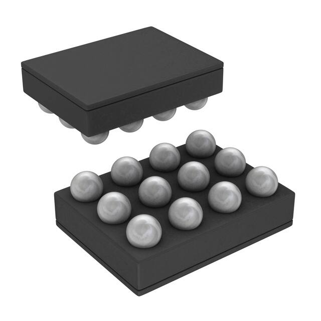
LM3561
www.ti.com
SNOSB44C – MARCH 2011 – REVISED MAY 2013
Synchronous Boost Converter
With 600-mA High-Side LED Driver and I2C-Compatible Interface
Check for Samples: LM3561
FEATURES
1
•
2
•
•
•
•
•
•
•
•
•
•
•
•
High-Side Current Source Allows Grounded
LED Cathode
Up to 90% Efficient
Ultra-Small Solution Size: VIN) the inductor will typically be the biggest area of efficiency
loss in the circuit. Therefore, choosing an inductor with the lowest possible series resistance is important.
Additionally, the saturation rating of the inductor should be greater than the maximum operating peak current of
the LM3561. This prevents excess efficiency loss that can occur with inductors that operate in saturation. For
proper inductor operation and circuit performance ensure that the inductor saturation and the peak current limit
setting of the LM3561 is greater than IPEAK. This can be calculated by:
28
Submit Documentation Feedback
Copyright © 2011–2013, Texas Instruments Incorporated
Product Folder Links: LM3561
�LM3561
www.ti.com
IPEAK =
SNOSB44C – MARCH 2011 – REVISED MAY 2013
I LOAD VOUT
V x (VOUT - VIN)
x
+ 'IL where 'IL = IN
K
VIN
2 x f SW x L x VOUT
(3)
ƒSW = 2MHz, and η can be found in the Typical Performance Characteristics plots.
Table 15. Recommended Inductors
Manufacturer
L
Part Number
Dimensions (L×W×H)
RDC
ISAT
Coilcraft
1µH
XPL2010-102ML
2mm×1.9mm×1mm
81mΩ
1.6A
TDK
1µH
VLS252012T-1R0N
2mm×2.5mm×1.2mm
73mΩ
2.7A
TDK
1µH
VLS2010-1R0N
2mm x 2mm x 1mm
90mΩ
1.65A
TDK
1µH
VLS2012ET-1R0N
2mm x 2mm x 1.2mm
71mΩ
1.65A
TDK
1µH
VLS20160ET-1R0N
2mm x 1.6mm x 0.95mm
100mΩ
1.5A
TDK
1µH
VLS252010ET-1R0N
2.5mm x 2mm x 1mm
70mΩ
1.9A
NTC THERMISTOR SELECTION
Programming bit [4] of Configuration Register 1 with a (1) selects Thermal Comparator mode, making the
LEDI/NTC pin a comparator input for flash LED thermal sensing. The thermal sensing circuit consists of a
negative temperature coefficient (NTC) thermistor and a series resistor which forms a resistive divider (see
Figure 38).
VIN
IN
SW
OUT
LM3561
VBIAS
NTC
SDA
RBIAS
LED
SCL
R(T)
GND
Low Thermal
Resistance
Between LED
and R(T)
Figure 38. NTC Circuit
The NTC thermistor senses the LEDs temperature via conducting the LEDs heat into the NTC thermistor. Heat
conduction is improved with a galvanic connection at GND (LED cathode and NTC thermistor GND terminal) and
by placing the thermistor in very close proximity to the flash LED.
NTC thermistors have a temperature to resistance relationship of:
E
R(T) = R25°C x e
§ 1 - 1·
©T °C+ 273 298¹
(4)
where β is given in the thermistor datasheet and R25C is the thermistor's value at +25°C. RBIAS is chosen so that
it is equal to:
R BIAS =
RT( TRIP) (VBIAS - VTRIP )
VTRIP
(5)
Submit Documentation Feedback
Copyright © 2011–2013, Texas Instruments Incorporated
Product Folder Links: LM3561
29
�LM3561
SNOSB44C – MARCH 2011 – REVISED MAY 2013
www.ti.com
where R(T)TRIP is the thermistor's value at the temperature trip point, VBIAS is the bias voltage for the thermistor
circuit, and VTRIP = 1V (typical). Choosing RBIAS here gives a more linear response around the temperature trip
voltage. For example with VBIAS = 1.8V and a thermistor whose nominal value at +25°C is 10kΩ and a β =
3380K, the trip point is chosen to be +93°C. The value of R(T) at 93°C is:
RBIAS is then:
º
»
¼
R(T) = 10 k : x e
E
º
1
- 1
93 + 273 298 »¼
= 1.215 k:
1.215 k: x (1.8 V - 1V)
= 972:
1V
(6)
Figure 39 shows the linearity of the thermistor resistive divider of the previous example.
2
1.8
1.6
VLED/NTC (V)
1.4
1.2
1
0.8
0.6
0.4
0.2
0
30
60
50
60
70
80
90
100
Temperature (°C)
Figure 39. Thermistor Resistive Divider Response vs Temperature
VLEDI/NTC vs Temp (VBIAS = 1.8V, THERMISTOR = 10kΩ at +25C, β = 3380, RBIAS =972Ω)
Another useful equation for the thermistor resistive divider is developed by combining the equations for RBIAS,
and R(T) and solving for temperature. This gives the following relationship.
E x 298 °C
- 273°C
T( °C) =
VTRIP x RBIAS
ª
º
E
298°C x LN
«(VBIAS - VTRIP ) x R25 °C» +
¬
¼
(7)
Using a spreadsheet such as Excel, different curves for the temperature trip point T(°C) can be created vs RBIAS,
Beta, or VBIAS in order to help better choose the thermal components for practical values of thermistors, series
resistors (R3), or reference voltages VBIAS.
NTC THERMISTOR PLACEMENT
The termination of the thermistor must be done directly to the cathode of the Flash LED in order to adequately
couple the heat from the LED into the thermistor. Consequentially, the noisy environment generated from the
switching of the LM3561's boost converter can introduce noise from GND into the thermistor sensing input. To
filter out this noise it is necessary to place a 0.1µF or larger ceramic capacitor close to the LEDI/NTC pin. The
filter capacitor's return must also connect with a low-impedance trace, as close as possible to the GND pin of the
LM3561.
30
Submit Documentation Feedback
Copyright © 2011–2013, Texas Instruments Incorporated
Product Folder Links: LM3561
�LM3561
www.ti.com
SNOSB44C – MARCH 2011 – REVISED MAY 2013
Layout Recommendations
The high frequency and relatively large switching currents of the LM3561 make the choice of layout important.
The following steps should be used as a reference to ensure the device is stable and maintains proper voltage
and current regulation across its intended operating voltage and current range.
1. Place CIN on the top layer (same layer as the LM3561) and as close to the device as possible. The input
capacitor conducts the driver currents during the low-side MOSFET turn-on and turn-off and can see current
spikes over 500mA in amplitude. Connecting the input capacitor through short wide traces on both the IN
and GND terminals will reduce the inductive voltage spikes that occur during switching and which can corrupt
the VIN line.
2. Place COUT on the top layer (same layer as the LM3561) and as close as possible to the OUT and GND
terminal. The returns for both CIN and COUT should come together at one point, and as close to the GND pin
as possible. Connecting COUT through short wide traces will reduce the series inductance on the OUT and
GND terminals that can corrupt the VOUT and GND line and cause excessive noise in the device and
surrounding circuitry.
3. Connect the inductor on the top layer close to the SW pin. There should be a low-impedance connection
from the inductor to SW due to the large DC inductor current, and at the same time the area occupied by the
SW node should be small so as to reduce the capacitive coupling of the fast dV/dt present at SW that can
couple into nearby traces.
4. Avoid routing logic traces near the SW node so as to avoid any capacitively coupled voltages from SW onto
any high impedance logic lines such as TX1/TORCH/GPIO1, TX2/GPIO2/INT, HWEN, LEDI/NTC (NTC
mode), SDA, and SCL. A good approach is to insert an inner layer GND plane underneath the SW node and
between any nearby routed traces. This creates a shield from the electric field generated at SW.
5. Terminate the Flash LED cathode directly to the GND pin of the LM3561. If possible, route the LED return
with a dedicated path so as to keep the high amplitude LED current out of the GND plane. For a Flash LED
that is routed relatively far away from the LM3561, a good approach is to sandwich the forward and return
current paths over the top of each other on two adjacent layers. This will help in reducing the inductance of
the LED current paths.
6. The NTC Thermistor is intended to have its return path connected to the LED's cathode. This allows the
thermistor resistive divider voltage (VNTC) to trip the comparators threshold as VNTC is falling. Additionally, the
thermistor to LED cathode junction can have low thermal resistivity since both the LED and the thermistor
are electrically connected at GND. The draw back is that the thermistor's return will see the switching
currents from the LM3561's boost converter. Because of this, it is necessary to have a filter capacitor at the
NTC pin which terminates close to the GND of the LM3561 and which can conduct the switched currents to
GND.
Submit Documentation Feedback
Copyright © 2011–2013, Texas Instruments Incorporated
Product Folder Links: LM3561
31
�LM3561
SNOSB44C – MARCH 2011 – REVISED MAY 2013
www.ti.com
REVISION HISTORY
Changes from Revision B (April 2013) to Revision C
•
32
Page
Changed layout of National Data Sheet to TI format .......................................................................................................... 31
Submit Documentation Feedback
Copyright © 2011–2013, Texas Instruments Incorporated
Product Folder Links: LM3561
�PACKAGE OPTION ADDENDUM
www.ti.com
10-Dec-2020
PACKAGING INFORMATION
Orderable Device
Status
(1)
Package Type Package Pins Package
Drawing
Qty
Eco Plan
(2)
Lead finish/
Ball material
MSL Peak Temp
Op Temp (°C)
Device Marking
(3)
(4/5)
(6)
LM3561TME/NOPB
ACTIVE
DSBGA
YFQ
12
250
RoHS & Green
SNAGCU
Level-1-260C-UNLIM
-40 to 85
DV
LM3561TMX/NOPB
ACTIVE
DSBGA
YFQ
12
3000
RoHS & Green
SNAGCU
Level-1-260C-UNLIM
-40 to 85
DV
(1)
The marketing status values are defined as follows:
ACTIVE: Product device recommended for new designs.
LIFEBUY: TI has announced that the device will be discontinued, and a lifetime-buy period is in effect.
NRND: Not recommended for new designs. Device is in production to support existing customers, but TI does not recommend using this part in a new design.
PREVIEW: Device has been announced but is not in production. Samples may or may not be available.
OBSOLETE: TI has discontinued the production of the device.
(2)
RoHS: TI defines "RoHS" to mean semiconductor products that are compliant with the current EU RoHS requirements for all 10 RoHS substances, including the requirement that RoHS substance
do not exceed 0.1% by weight in homogeneous materials. Where designed to be soldered at high temperatures, "RoHS" products are suitable for use in specified lead-free processes. TI may
reference these types of products as "Pb-Free".
RoHS Exempt: TI defines "RoHS Exempt" to mean products that contain lead but are compliant with EU RoHS pursuant to a specific EU RoHS exemption.
Green: TI defines "Green" to mean the content of Chlorine (Cl) and Bromine (Br) based flame retardants meet JS709B low halogen requirements of
很抱歉,暂时无法提供与“LM3561TMX/NOPB”相匹配的价格&库存,您可以联系我们找货
免费人工找货