Order
Now
Product
Folder
Support &
Community
Tools &
Software
Technical
Documents
LM35
ZHCSHC4H – AUGUST 1999 – REVISED DECEMBER 2017
LM35 高精度摄氏温度传感器
1 特性
•
•
•
•
•
•
•
•
•
•
•
1
3 说明
直接以摄氏温度(摄氏度)进行校准
线性 +10mV/°C 比例因子
0.5°C 的确保精度(25°C 时)
额定温度范围为 −55°C 至 150°C
适用于远程 应用
晶圆级修整实现低成本
工作电压范围 4V 至 30V
电流漏极小于 60μA
低自发热,处于静止的空气中时为 0.08°C
非线性典型值仅 ±¼°C
低阻抗输出,1mA 负载时为 0.1Ω
2 应用
•
•
•
•
电源
电池管理
HVAC
电器
LM35 系列产品是高精度集成电路温度器件,其输出电
压与摄氏温度成线性正比关系。相比于以开尔文温度校
准的线性温度传感器,LM35 器件的优势在于使用者无
需在输出电压中减去一个较大的恒定电压值即可便捷地
实现摄氏度调节。LM35 器件无需进行任何外部校准或
修整,可在室温下提供 ±¼°C 的典型精度,而在
−55°C 至 +150°C 的完整温度范围内提供 ±¾°C 的精
度。晶圆级的修正和校准可确保更低的成本。LM35 器
件具有低输出阻抗、线性输出和高精度内在校准功能,
这些特性使得连接读取或控制电路变得尤为简单。此器
件可使用单电源或正负电源供电。因为 LM35 器件仅
需从电源中消耗 60μA 的电流,所以处于静止的空气中
时具有不到 0.1°C 的极低自发热。LM35 器件额定工作
温度范围为 −55°C 至 150°C,LM35C 器件额定工作
温度范围 −40°C 至 110°C(−10° 时精度更高)。
LM35 系列器件采用密封 TO 晶体管封装,LM35C、
LM35CA 和 LM35D 器件采用塑料 TO-92 晶体管封
装。LM35D 器件采用 8 引线表面贴装小外形封装和塑
料 TO-220 封装。
器件信息(1)
器件型号
LM35
封装
封装尺寸(标称值)
TO-CAN (3)
4.699mm × 4.699mm
TO-92 (3)
4.30mm × 4.30mm
SOIC (8)
4.90mm x 3.91mm
TO-220 (3)
14.986mm × 10.16mm
(1) 如需了解所有可用封装,请参阅数据表末尾的可订购产品附
录。
基本摄氏温度传感器
(2°C 至 150°C)
)
全范围摄氏温度传感器
+VS
+VS
(4 V to 20 V)
LM35
LM35
VOUT
OUTPUT
0 mV + 10.0 mV/°C
R1
tVS
选择 R1 = –VS/50µA
150°C 时,VOUT = 1500mV
25°C 时,VOUT = 250mV
–55°C 时,VOUT = –550mV
1
An IMPORTANT NOTICE at the end of this data sheet addresses availability, warranty, changes, use in safety-critical applications,
intellectual property matters and other important disclaimers. PRODUCTION DATA.
English Data Sheet: SNIS159
�LM35
ZHCSHC4H – AUGUST 1999 – REVISED DECEMBER 2017
www.ti.com.cn
目录
1
2
3
4
5
6
特性 ..........................................................................
应用 ..........................................................................
说明 ..........................................................................
修订历史记录 ...........................................................
Pin Configuration and Functions .........................
Specifications.........................................................
1
1
1
2
3
4
6.1
6.2
6.3
6.4
6.5
6.6
6.7
Absolute Maximum Ratings ...................................... 4
ESD Ratings.............................................................. 4
Recommended Operating Conditions....................... 4
Thermal Information .................................................. 4
Electrical Characteristics: LM35A, LM35CA Limits... 5
Electrical Characteristics: LM35A, LM35CA ............. 6
Electrical Characteristics: LM35, LM35C, LM35D
Limits.......................................................................... 8
6.8 Electrical Characteristics: LM35, LM35C, LM35D ... 9
6.9 Typical Characteristics ............................................ 11
7
Detailed Description ............................................ 13
7.1 Overview ................................................................. 13
7.2 Functional Block Diagram ....................................... 13
7.3 Feature Description................................................. 13
7.4 Device Functional Modes........................................ 13
8
Application and Implementation ........................ 14
8.1 Application Information............................................ 14
8.2 Typical Application .................................................. 15
8.3 System Examples ................................................... 16
9 Power Supply Recommendations...................... 19
10 Layout................................................................... 19
10.1 Layout Guidelines ................................................. 19
10.2 Layout Example .................................................... 20
11 器件和文档支持 ..................................................... 21
11.1
11.2
11.3
11.4
11.5
接收文档更新通知 .................................................
社区资源................................................................
商标 .......................................................................
静电放电警告.........................................................
Glossary ................................................................
21
21
21
21
21
12 机械、封装和可订购信息 ....................................... 21
4 修订历史记录
Changes from Revision G (August 2016) to Revision H
Page
•
Changed NDV Package (TO-CAN) pinout from bottom view back to top view; added textnote to pinout............................. 3
•
Added pin numbers to the TO-CAN (TO46) pinout ................................................................................................................ 3
Changes from Revision F (January 2016) to Revision G
Page
•
Equation 1, changed From: 10 mV/°F To: 10mv/°C ............................................................................................................ 13
•
Power Supply Recommendations, changed From: "4-V to 5.5-V power supply" To: "4-V to 30-V power supply: .............. 19
Changes from Revision E (January 2015) to Revision F
•
Changed NDV Package (TO-CAN) pinout from Top View to Bottom View ........................................................................... 3
Changes from Revision D (October 2013) to Revision E
•
Page
Page
已添加 引脚配置和功能 部分、ESD 额定值表、特性 说明 部分、器件功能模式、应用和实施 部分、电源相关建议 部
分、布局 部分、器件和文档支持 部分以及机械、封装和可订购信息 部分 ............................................................................. 1
Changes from Revision C (July 2013) to Revision D
Page
•
已更改 将 W更改为 Ω 添加了.................................................................................................................................................. 1
•
Changed W to Ω in Abs Max tablenote. ................................................................................................................................ 4
2
Copyright © 1999–2017, Texas Instruments Incorporated
�LM35
www.ti.com.cn
ZHCSHC4H – AUGUST 1999 – REVISED DECEMBER 2017
5 Pin Configuration and Functions
NDV Package
3-Pin TO-CAN
(Top View)
LP Package
3-Pin TO-92
(Bottom View)
(1) +VS (3) GND
+VS VOUT GND
(2) VOUT
1
2
3
Case is connected to negative pin (GND)
Refer the second NDV0003H page for
reference
NEB Package
3-Pin TO-220
(Top View)
D Package
8-PIN SOIC
(Top View)
VOUT
N.C.
1
2
8
7
+VS
N.C.
N.C.
3
6
N.C.
GND
4
5
N.C.
LM
35DT
1
2
3
N.C. = No connection
+VS
GND
VOUT
Tab is connected to the negative pin
(GND).
NOTE: The LM35DT pinout is different than
the discontinued LM35DP
Pin Functions
PIN
NAME
VOUT
N.C.
GND
N.C.
+VS
TO46
TO92
TO220
SO8
2
2
3
1
—
—
—
2
—
—
—
3
3
3
2
4
—
—
—
5
—
—
—
6
—
—
—
7
1
1
1
8
Copyright © 1999–2017, Texas Instruments Incorporated
TYPE
DESCRIPTION
O
Temperature Sensor Analog Output
—
No Connection
GROUND
—
POWER
Device ground pin, connect to power supply negative
terminal
No Connection
Positive power supply pin
3
�LM35
ZHCSHC4H – AUGUST 1999 – REVISED DECEMBER 2017
www.ti.com.cn
6 Specifications
6.1 Absolute Maximum Ratings
over operating free-air temperature range (unless otherwise noted) (1) (2)
MIN
MAX
UNIT
Supply voltage
–0.2
35
V
Output voltage
–1
6
V
Output current
10
mA
Maximum Junction Temperature, TJmax
150
°C
Storage Temperature, Tstg
(1)
(2)
TO-CAN, TO-92 Package
–60
150
TO-220, SOIC Package
–65
150
°C
If Military/Aerospace specified devices are required, please contact the Texas Instruments Sales Office/ Distributors for availability and
specifications.
Absolute Maximum Ratings indicate limits beyond which damage to the device may occur. DC and AC electrical specifications do not
apply when operating the device beyond its rated operating conditions.
6.2 ESD Ratings
V(ESD)
(1)
Electrostatic discharge
Human-body model (HBM), per ANSI/ESDA/JEDEC JS-001 (1)
VALUE
UNIT
±2500
V
JEDEC document JEP155 states that 500-V HBM allows safe manufacturing with a standard ESD control process.
6.3 Recommended Operating Conditions
over operating free-air temperature range (unless otherwise noted)
Specified operating temperature: TMIN to
TMAX
MIN
MAX
LM35, LM35A
–55
150
LM35C, LM35CA
–40
110
0
100
4
30
LM35D
Supply Voltage (+VS)
UNIT
°C
V
6.4 Thermal Information
LM35
THERMAL METRIC (1) (2)
NDV
LP
3 PINS
RθJA
Junction-to-ambient thermal resistance
RθJC(top) Junction-to-case (top) thermal resistance
(1)
(2)
4
D
NEB
8 PINS
3 PINS
400
180
220
90
24
—
—
—
UNIT
°C/W
For more information about traditional and new thermal metrics, see the IC Package Thermal Metrics application report, SPRA953.
For additional thermal resistance information, see Typical Application.
Copyright © 1999–2017, Texas Instruments Incorporated
�LM35
www.ti.com.cn
ZHCSHC4H – AUGUST 1999 – REVISED DECEMBER 2017
6.5 Electrical Characteristics: LM35A, LM35CA Limits
Unless otherwise noted, these specifications apply: −55°C ≤ TJ ≤ 150°C for the LM35 and LM35A; −40°C ≤ TJ ≤ 110°C for the
LM35C and LM35CA; and 0°C ≤ TJ ≤ 100°C for the LM35D. VS = 5 Vdc and ILOAD = 50 μA, in the circuit of Full-Range
Centigrade Temperature Sensor. These specifications also apply from 2°C to TMAX in the circuit of Figure 14.
LM35A
PARAMETER
Accuracy (3)
TEST CONDITIONS
LM35CA
TYP
TESTED
LIMIT (1)
DESIGN
LIMIT (2)
TYP
TESTED
LIMIT (1)
±0.2
TA = 25°C
±0.2
±0.5
TA = –10°C
±0.3
±0.5
TA = TMAX
±0.4
±1
±0.4
TA = TMIN
±0.4
±1
±0.4
±1.5
±0.15
±0.3
±0.3
DESIGN
LIMIT (2)
±1
±1
Nonlinearity (4)
TMIN ≤ TA ≤ TMAX,
–40°C ≤ TJ ≤ 125°C
Sensor gain
(average slope)
TMIN ≤ TA ≤ TMAX
10
9.9
10
9.9
–40°C ≤ TJ ≤ 125°C
10
10.1
10
10.1
TA = 25°C
±0.4
±1
±0.4
TMIN ≤ TA ≤ TMAX,
–40°C ≤ TJ ≤ 125°C
±0.5
Load regulation (5)
0 ≤ IL ≤ 1 mA
Line regulation (5)
TA = 25°C
±0.01
4 V ≤ VS ≤ 30 V,
–40°C ≤ TJ ≤ 125°C
±0.02
VS = 5 V, 25°C
Quiescent current (6)
Temperature
coefficient of
quiescent current
105
VS = 30 V, 25°C
56.2
(1)
(2)
(3)
(4)
(5)
(6)
±0.35
±3
±0.05
±0.1
67
68
±0.1
114
68
91.5
0.5
2
0.5
2
–40°C ≤ TJ ≤ 125°C
0.39
0.5
0.39
0.5
1.5
2
1.5
2
TJ = TMAX, for 1000 hours
±0.08
±0.08
mV/mA
mV/V
µA
116
4 V ≤ VS ≤ 30 V,
–40°C ≤ TJ ≤ 125°C
0.2
mV/°C
67
0.2
1
°C
±0.05
91
56.2
133
±3
±0.02
56
131
105.5
±0.5
±0.01
°C
±1
4 V ≤ VS ≤ 30 V, 25°C
Minimum temperature
In circuit of Figure 14, IL = 0
for rate accuracy
Long term stability
56
VS = 5 V, –40°C ≤ TJ ≤ 125°C
VS = 30 V, –40°C ≤ TJ ≤ 125°C
Change of quiescent
current (5)
±0.18
UNIT
1
µA
µA/°C
°C
°C
Tested Limits are ensured and 100% tested in production.
Design Limits are ensured (but not 100% production tested) over the indicated temperature and supply voltage ranges. These limits are
not used to calculate outgoing quality levels.
Accuracy is defined as the error between the output voltage and 10 mv/°C times the case temperature of the device, at specified
conditions of voltage, current, and temperature (expressed in °C).
Non-linearity is defined as the deviation of the output-voltage-versus-temperature curve from the best-fit straight line, over the rated
temperature range of the device.
Regulation is measured at constant junction temperature, using pulse testing with a low duty cycle. Changes in output due to heating
effects can be computed by multiplying the internal dissipation by the thermal resistance.
Quiescent current is defined in the circuit of Figure 14.
Copyright © 1999–2017, Texas Instruments Incorporated
5
�LM35
ZHCSHC4H – AUGUST 1999 – REVISED DECEMBER 2017
www.ti.com.cn
6.6 Electrical Characteristics: LM35A, LM35CA
Unless otherwise noted, these specifications apply: −55°C ≤ TJ ≤ 150°C for the LM35 and LM35A; −40°C ≤ TJ ≤ 110°C for the
LM35C and LM35CA; and 0°C ≤ TJ ≤ 100°C for the LM35D. VS = 5 Vdc and ILOAD = 50 μA, in the circuit of Full-Range
Centigrade Temperature Sensor. These specifications also apply from 2°C to TMAX in the circuit of Figure 14.
PARAMETER
LM35A
TEST CONDITIONS
MIN
TYP
LM35CA
MAX
±0.2
TA = 25°C
Tested Limit
(2)
TYP
TYP
MAX
UNIT
±0.2
±0.5
±0.5
Design Limit (3)
TA = –10°C
Tested Limit
±0.3
±0.3
±0.4
±0.4
(2)
Design Limit (3)
Accuracy (1)
TA = TMAX
±1
Tested Limit (2)
Design Limit
±1
±1
(3)
±0.4
TA = TMIN
Tested Limit (2)
±0.4
±1
Design Limit (3)
±1.5
±0.18
TMIN ≤ TA ≤ TMAX,
–40°C ≤ TJ ≤ 125°C
Nonlinearity (4)
±0.15
Tested Limit (2)
Design Limit
°C
(3)
±0.35
10
TMIN ≤ TA ≤ TMAX
Tested Limit (2)
±0.3
10
9.9
Design Limit (3)
Sensor gain
(average slope)
9.9
10
–40°C ≤ TJ ≤ 125°C
Tested Limit (2)
10
10.1
±0.4
Load regulation
0 ≤ IL ≤ 1 mA
Tested Limit (2)
±0.4
±1
±0.5
TMIN ≤ TA ≤ TMAX,
–40°C ≤ TJ ≤ 125°C
TA = 25°C
Tested Limit (2)
Design Limit (3)
±3
(5)
6
±0.05
±0.02
4 V ≤ VS ≤ 30 V,
–40°C ≤ TJ ≤ 125°C
(4)
Tested Limit (2)
±3
±0.01
±0.05
Design Limit (3)
Line regulation (5)
(2)
(3)
mV/mA
±0.5
±0.01
(1)
±1
Design Limit (3)
(5)
mV/°C
10.1
Design Limit (3)
TA = 25°C
°C
mV/V
±0.02
Tested Limit (2)
Design Limit (3)
±0.1
±0.1
Accuracy is defined as the error between the output voltage and 10 mv/°C times the case temperature of the device, at specified
conditions of voltage, current, and temperature (expressed in °C).
Tested Limits are ensured and 100% tested in production.
Design Limits are ensured (but not 100% production tested) over the indicated temperature and supply voltage ranges. These limits are
not used to calculate outgoing quality levels.
Non-linearity is defined as the deviation of the output-voltage-versus-temperature curve from the best-fit straight line, over the rated
temperature range of the device.
Regulation is measured at constant junction temperature, using pulse testing with a low duty cycle. Changes in output due to heating
effects can be computed by multiplying the internal dissipation by the thermal resistance.
Copyright © 1999–2017, Texas Instruments Incorporated
�LM35
www.ti.com.cn
ZHCSHC4H – AUGUST 1999 – REVISED DECEMBER 2017
Electrical Characteristics: LM35A, LM35CA (continued)
Unless otherwise noted, these specifications apply: −55°C ≤ TJ ≤ 150°C for the LM35 and LM35A; −40°C ≤ TJ ≤ 110°C for the
LM35C and LM35CA; and 0°C ≤ TJ ≤ 100°C for the LM35D. VS = 5 Vdc and ILOAD = 50 μA, in the circuit of Full-Range
Centigrade Temperature Sensor. These specifications also apply from 2°C to TMAX in the circuit of Figure 14.
PARAMETER
LM35A
TEST CONDITIONS
MIN
TYP
LM35CA
MAX
56
VS = 5 V, 25°C
Tested Limit
(2)
TYP
TYP
MAX
UNIT
56
67
67
Design Limit (3)
105
VS = 5 V,
–40°C ≤ TJ ≤ 125°C
Quiescent
current (6)
Tested Limit
91
(2)
Design Limit (3)
131
56.2
VS = 30 V, 25°C
Tested Limit (2)
114
56.2
68
µA
68
Design Limit (3)
105.5
VS = 30 V,
–40°C ≤ TJ ≤ 125°C
91.5
Tested Limit (2)
Design Limit (3)
133
0.2
4 V ≤ VS ≤ 30 V, 25°C
Change of
quiescent
current (5)
Design Limit
1
4 V ≤ VS ≤ 30 V,
–40°C ≤ TJ ≤ 125°C
Minimum
temperature for
rate accuracy
In circuit of Figure 14, IL =
0
Long term
stability
TJ = TMAX, for 1000 hours
µA
0.5
Tested Limit (2)
Design Limit (3)
2
0.39
–40°C ≤ TJ ≤ 125°C
1
(3)
0.5
Temperature
coefficient of
quiescent current
(6)
Tested Limit (2)
116
0.2
2
0.39
Tested Limit (2)
µA/°C
Design Limit (3)
0.5
1.5
0.5
1.5
Tested Limit (2)
°C
Design Limit (3)
2
±0.08
2
±0.08
°C
Quiescent current is defined in the circuit of Figure 14.
Copyright © 1999–2017, Texas Instruments Incorporated
7
�LM35
ZHCSHC4H – AUGUST 1999 – REVISED DECEMBER 2017
www.ti.com.cn
6.7 Electrical Characteristics: LM35, LM35C, LM35D Limits
Unless otherwise noted, these specifications apply: −55°C ≤ TJ ≤ 150°C for the LM35 and LM35A; −40°C ≤ TJ ≤ 110°C for the
LM35C and LM35CA; and 0°C ≤ TJ ≤ 100°C for the LM35D. VS = 5 Vdc and ILOAD = 50 μA, in the circuit of Full-Range
Centigrade Temperature Sensor. These specifications also apply from 2°C to TMAX in the circuit of Figure 14.
LM35
PARAMETER
Accuracy, LM35,
LM35C (3)
Accuracy, LM35D (3)
Nonlinearity (4)
Sensor gain
(average slope)
Load regulation (5)
0 ≤ IL ≤ 1 mA
Line regulation (5)
TEST CONDITIONS
TYP
TESTED
LIMIT (1)
TA = 25°C
±0.4
±1
TA = –10°C
±0.5
TA = TMAX
±0.8
TA = TMIN
±0.8
Temperature
coefficient of
quiescent current
(1)
(2)
(3)
(4)
(5)
(6)
8
±0.4
±1
DESIGN
LIMIT (2)
±0.5
±1.5
±0.8
±1.5
±0.8
±2
±0.6
±0.9
±2
TA = TMIN
±0.9
±2
±0.2
±0.5
±0.3
TMIN ≤ TA ≤ TMAX,
–40°C ≤ TJ ≤ 125°C
10
9.8
10
9.8
10
10.2
10
10.2
TA = 25°C
±0.4
±2
±0.4
TMIN ≤ TA ≤ TMAX,
–40°C ≤ TJ ≤ 125°C
±0.5
TA = 25°C
±0.01
4 V ≤ VS ≤ 30 V,
–40°C ≤ TJ ≤ 125°C
±0.02
56
VS = 5 V, –40°C ≤ TJ ≤ 125°C
105
VS = 30 V, 25°C
56.2
±0.5
±5
±0.1
±0.2
80
82
105.5
±0.2
138
82
91.5
4 V ≤ VS ≤ 30 V,
–40°C ≤ TJ ≤ 125°C
0.5
3
0.5
3
–40°C ≤ TJ ≤ 125°C
0.39
0.7
0.39
0.7
1.5
2
1.5
2
TJ = TMAX, for 1000 hours
±0.08
±0.08
mV/°C
mV/mA
mV/V
µA
141
0.2
0.2
°C
80
4 V ≤ VS ≤ 30 V, 25°C
2
°C
±0.1
91
56.2
161
±5
±0.02
56
158
°C
±2
±0.5
±0.01
UNIT
±1.5
TMIN ≤ TA ≤ TMAX,
–40°C ≤ TJ ≤ 125°C
Minimum temperature
In circuit of Figure 14, IL = 0
for rate accuracy
Long term stability
±1.5
TESTED
LIMIT (1)
TA = TMAX
VS = 30 V, –40°C ≤ TJ ≤ 125°C
Change of quiescent
current (5)
±1.5
TYP
TA = 25°C
VS = 5 V, 25°C
Quiescent current (6)
LM35C, LM35D
DESIGN
LIMIT (2)
2
µA
µA/°C
°C
°C
Tested Limits are ensured and 100% tested in production.
Design Limits are ensured (but not 100% production tested) over the indicated temperature and supply voltage ranges. These limits are
not used to calculate outgoing quality levels.
Accuracy is defined as the error between the output voltage and 10 mv/°C times the case temperature of the device, at specified
conditions of voltage, current, and temperature (expressed in °C).
Non-linearity is defined as the deviation of the output-voltage-versus-temperature curve from the best-fit straight line, over the rated
temperature range of the device.
Regulation is measured at constant junction temperature, using pulse testing with a low duty cycle. Changes in output due to heating
effects can be computed by multiplying the internal dissipation by the thermal resistance.
Quiescent current is defined in the circuit of Figure 14.
Copyright © 1999–2017, Texas Instruments Incorporated
�LM35
www.ti.com.cn
ZHCSHC4H – AUGUST 1999 – REVISED DECEMBER 2017
6.8 Electrical Characteristics: LM35, LM35C, LM35D
Unless otherwise noted, these specifications apply: −55°C ≤ TJ ≤ 150°C for the LM35 and LM35A; −40°C ≤ TJ ≤ 110°C for the
LM35C and LM35CA; and 0°C ≤ TJ ≤ 100°C for the LM35D. VS = 5 Vdc and ILOAD = 50 μA, in the circuit of Full-Range
Centigrade Temperature Sensor. These specifications also apply from 2°C to TMAX in the circuit of Figure 14.
PARAMETER
LM35
TEST CONDITIONS
MIN
TYP
LM35C, LM35D
MAX
±0.4
TA = 25°C
Tested Limit
(2)
MIN
TYP
MAX
UNIT
±0.4
±1
±1
Design Limit (3)
TA = –10°C
Tested Limit
±0.5
±0.5
±0.8
±0.8
(2)
Design Limit (3)
Accuracy, LM35,
LM35C (1)
TA = TMAX
±1.5
Tested Limit (2)
Design Limit
±1.5
(3)
±1.5
±0.8
TA = TMIN
°C
±0.8
Tested Limit (2)
Design Limit (3)
±1.5
±2
±0.6
TA = 25°C
Tested Limit (2)
Design Limit
±1.5
(3)
±0.9
Accuracy,
LM35D (1)
TA = TMAX
Tested Limit (2)
°C
Design Limit (3)
±2
±0.9
TA = TMIN
Tested Limit (2)
Design Limit (3)
±2
±0.3
Nonlinearity (4)
TMIN ≤ TA ≤ TMAX,
–40°C ≤ TJ ≤ 125°C
±0.2
Tested Limit (2)
°C
Design Limit (3)
±0.5
10
TMIN ≤ TA ≤ TMAX,
–40°C ≤ TJ ≤ 125°C
Sensor gain
(average slope)
Tested Limit (2)
±0.5
10
9.8
Design Limit (3)
9.8
10
Tested Limit (2)
10
10.2
Design Limit (3)
10.2
±0.4
TA = 25°C
(2)
(3)
(4)
(5)
±2
±0.5
TMIN ≤ TA ≤ TMAX,
–40°C ≤ TJ ≤ 125°C
(1)
Tested Limit (2)
±0.4
±2
Design Limit (3)
Load regulation (5)
0 ≤ IL ≤ 1 mA
mV/°C
mV/mA
±0.5
Tested Limit (2)
Design Limit (3)
±5
±5
Accuracy is defined as the error between the output voltage and 10 mv/°C times the case temperature of the device, at specified
conditions of voltage, current, and temperature (expressed in °C).
Tested Limits are ensured and 100% tested in production.
Design Limits are ensured (but not 100% production tested) over the indicated temperature and supply voltage ranges. These limits are
not used to calculate outgoing quality levels.
Non-linearity is defined as the deviation of the output-voltage-versus-temperature curve from the best-fit straight line, over the rated
temperature range of the device.
Regulation is measured at constant junction temperature, using pulse testing with a low duty cycle. Changes in output due to heating
effects can be computed by multiplying the internal dissipation by the thermal resistance.
Copyright © 1999–2017, Texas Instruments Incorporated
9
�LM35
ZHCSHC4H – AUGUST 1999 – REVISED DECEMBER 2017
www.ti.com.cn
Electrical Characteristics: LM35, LM35C, LM35D (continued)
Unless otherwise noted, these specifications apply: −55°C ≤ TJ ≤ 150°C for the LM35 and LM35A; −40°C ≤ TJ ≤ 110°C for the
LM35C and LM35CA; and 0°C ≤ TJ ≤ 100°C for the LM35D. VS = 5 Vdc and ILOAD = 50 μA, in the circuit of Full-Range
Centigrade Temperature Sensor. These specifications also apply from 2°C to TMAX in the circuit of Figure 14.
PARAMETER
LM35
TEST CONDITIONS
MIN
TYP
LM35C, LM35D
MAX
±0.01
TA = 25°C
Tested Limit
(2)
MIN
TYP
±0.1
±0.1
±0.02
4 V ≤ VS ≤ 30 V,
–40°C ≤ TJ ≤ 125°C
±0.02
mV/V
Tested Limit (2)
Design Limit (3)
±0.2
56
VS = 5 V, 25°C
UNIT
±0.01
Design Limit (3)
Line regulation (5)
MAX
Tested Limit (2)
±0.2
56
80
80
Design Limit (3)
105
VS = 5 V, –40°C ≤ TJ ≤
125°C
Quiescent
current (6)
91
Tested Limit (2)
Design Limit (3)
158
56.2
VS = 30 V, 25°C
Tested Limit (2)
Design Limit
82
Change of
quiescent
current (5)
Design Limit (3)
91.5
161
µA
0.5
Tested Limit (2)
Design Limit (3)
3
0.39
–40°C ≤ TJ ≤ 125°C
Minimum
temperature for
rate accuracy
In circuit of Figure 14, IL = 0 Tested Limit (2)
Long term
stability
TJ = TMAX, for 1000 hours
10
2
2
0.5
Temperature
coefficient of
quiescent current
(6)
141
0.2
Tested Limit (2)
Design Limit (3)
4 V ≤ VS ≤ 30 V,
–40°C ≤ TJ ≤ 125°C
82
Tested Limit (2)
0.2
4 V ≤ VS ≤ 30 V, 25°C
µA
(3)
105.5
VS = 30 V,
–40°C ≤ TJ ≤ 125°C
138
56.2
3
0.39
Tested Limit (2)
µA/°C
Design Limit (3)
0.7
1.5
0.7
1.5
°C
Design Limit (3)
2
±0.08
2
±0.08
°C
Quiescent current is defined in the circuit of Figure 14.
Copyright © 1999–2017, Texas Instruments Incorporated
�LM35
www.ti.com.cn
ZHCSHC4H – AUGUST 1999 – REVISED DECEMBER 2017
6.9 Typical Characteristics
45
40
TIME CONSTANT (SEC)
THERMAL RESISTANCE (ƒC/W)
400
300
200
T0-46
100
35
30
25
20
T0-46
15
10
T0-92
5
T0-92
0
0
0
400
800
1200
1600
0
2000
AIR VELOCITY (FPM)
1200
1600
2000
C002
Figure 2. Thermal Time Constant
120
PERCENT OF FINAL VALUE (%)
120
PERCENT OF FINAL VALUE (%)
800
AIR VELOCITY (FPM)
Figure 1. Thermal Resistance Junction To Air
100
80
60
40
20
0
±20
100
80
T0-46
60
T0-92
40
20
0
±20
0
2
4
6
8
TIME (MINUTES)
0
2
Figure 3. Thermal Response In Still Air
4
6
TIME (SEC)
C003
8
C004
Figure 4. Thermal Response In Stirred Oil Bath
4.4
160
4.2
TYPICAL
IOUT = 2.0 mA
4.0
140
QUIESCENT CURRENT ( A)
SUPPLY VOLTAGE (V)
400
C001
3.8
3.6
3.4
TYPICAL
IOUT = 1.0 mA
3.2
3.0
TYPICAL
IOUT = 0 A or 50 A
2.8
120
100
80
60
40
20
2.6
2.4
0
±75
±25
25
75
125
TEMPERATURE (ƒC)
175
C005
Figure 5. Minimum Supply Voltage vs Temperature
Copyright © 1999–2017, Texas Instruments Incorporated
±75
±25
25
75
TEMPERATURE (ƒC)
125
175
C006
Figure 6. Quiescent Current vs Temperature (in Circuit of
Figure 14)
11
�LM35
ZHCSHC4H – AUGUST 1999 – REVISED DECEMBER 2017
www.ti.com.cn
200
2.0
180
1.5
TEMPERATURE ERROR (ƒC)
QUIESCENT CURRENT ( A)
Typical Characteristics (continued)
160
140
120
100
80
0.5
±0.5
±2.0
25
75
125
LM35A
±1.0
40
±25
LM35A
TYPICAL
0.0
±1.5
175
TEMPERATURE (ƒC)
LM35
±75
25
±25
75
125
TEMPERATURE (ƒC)
C007
Figure 7. Quiescent Current vs Temperature (in Circuit of
Full-Range Centigrade Temperature Sensor)
175
C008
Figure 8. Accuracy vs Temperature (Ensured)
1600
2.5
LM35D
2.0
1400
LM35C
1.5
1200
1.0
Noise (nV/—Hz)
TEMPERATURE ERROR (ƒC)
1.0
60
±75
LM35
LM35CA
0.5
TYPICAL
0.0
±0.5
LM35CA
1000
±1.0
800
600
400
±1.5
LM35C
200
±2.0
0
±2.5
±75
±25
25
75
125
10
175
TEMPERATURE (ƒC)
100
1k
10k
FREQUENCY (Hz)
C009
100k
C010
Figure 10. Noise Voltage
Figure 9. Accuracy vs Temperature (Ensured)
VIN (V)
6
4
2
0
0.6
VOUT (V)
0.4
0.2
0
-0.2
-20
-10
0
10
20
30
40
50
TIME ( SEC)
60
C011
Figure 11. Start-Up Response
12
Copyright © 1999–2017, Texas Instruments Incorporated
�LM35
www.ti.com.cn
ZHCSHC4H – AUGUST 1999 – REVISED DECEMBER 2017
7 Detailed Description
7.1 Overview
The LM35-series devices are precision integrated-circuit temperature sensors, with an output voltage linearly
proportional to the Centigrade temperature. The LM35 device has an advantage over linear temperature sensors
calibrated in Kelvin, as the user is not required to subtract a large constant voltage from the output to obtain
convenient Centigrade scaling. The LM35 device does not require any external calibration or trimming to provide
typical accuracies of ± ¼ °C at room temperature and ± ¾ °C over a full −55°C to 150°C temperature range.
Lower cost is assured by trimming and calibration at the wafer level. The low output impedance, linear output,
and precise inherent calibration of the LM35 device makes interfacing to readout or control circuitry especially
easy. The device is used with single power supplies, or with plus and minus supplies. As the LM35 device draws
only 60 μA from the supply, it has very low self-heating of less than 0.1°C in still air. The LM35 device is rated to
operate over a −55°C to 150°C temperature range, while the LM35C device is rated for a −40°C to 110°C range
(−10° with improved accuracy). The temperature-sensing element is comprised of a delta-V BE architecture.
The temperature-sensing element is then buffered by an amplifier and provided to the VOUT pin. The amplifier
has a simple class A output stage with typical 0.5-Ω output impedance as shown in the Functional Block
Diagram. Therefore the LM35 can only source current and it's sinking capability is limited to 1 μA.
7.2 Functional Block Diagram
A1
1.38 VPTAT
+VS
nR1
Q1
Q2
10E
+
A2
E
VOUT = 10 mV/°C
V0
.125 R2
nR1
8.8 mV/°C
i
R2
7.3 Feature Description
7.3.1 LM35 Transfer Function
The accuracy specifications of the LM35 are given with respect to a simple linear transfer function:
VOUT = 10 mv/°C × T
where
•
•
VOUT is the LM35 output voltage
T is the temperature in °C
(1)
7.4 Device Functional Modes
The only functional mode of the LM35 is that it has an analog output directly proportional to temperature.
Copyright © 1999–2017, Texas Instruments Incorporated
13
�LM35
ZHCSHC4H – AUGUST 1999 – REVISED DECEMBER 2017
www.ti.com.cn
8 Application and Implementation
NOTE
Information in the following applications sections is not part of the TI component
specification, and TI does not warrant its accuracy or completeness. TI’s customers are
responsible for determining suitability of components for their purposes. Customers should
validate and test their design implementation to confirm system functionality.
8.1 Application Information
The features of the LM35 make it suitable for many general temperature sensing applications. Multiple package
options expand on it's flexibility.
8.1.1 Capacitive Drive Capability
Like most micropower circuits, the LM35 device has a limited ability to drive heavy capacitive loads. Alone, the
LM35 device is able to drive 50 pF without special precautions. If heavier loads are anticipated, isolating or
decoupling the load with a resistor is easy (see Figure 12). The tolerance of capacitance can be improved with a
series R-C damper from output to ground (see Figure 13).
When the LM35 device is applied with a 200-Ω load resistor as shown in Figure 16, Figure 17, or Figure 19, the
device is relatively immune to wiring capacitance because the capacitance forms a bypass from ground to input
and not on the output. However, as with any linear circuit connected to wires in a hostile environment,
performance is affected adversely by intense electromagnetic sources (such as relays, radio transmitters, motors
with arcing brushes, and SCR transients), because the wiring acts as a receiving antenna and the internal
junctions act as rectifiers. For best results in such cases, a bypass capacitor from VIN to ground and a series R-C
damper, such as 75 Ω in series with 0.2 or 1 μF from output to ground, are often useful. Examples are shown in
Figure 13, Figure 24, and Figure 25.
HEAVY CAPACITIVE LOAD, WIRING, ETC.
+
2k
LM35
TO A HIGH-IMPEDANCE LOAD
OUT
v
Figure 12. LM35 with Decoupling from Capacitive Load
HEAVY CAPACITIVE LOAD, WIRING, ETC.
+
LM35
0.01 PF BYPASS
OPTONAL
v
OUT
TO A HIGH-IMPEDANCE LOAD
75
1 PF
Figure 13. LM35 with R-C Damper
14
Copyright © 1999–2017, Texas Instruments Incorporated
�LM35
www.ti.com.cn
ZHCSHC4H – AUGUST 1999 – REVISED DECEMBER 2017
8.2 Typical Application
8.2.1 Basic Centigrade Temperature Sensor
+VS
(4 V to 20 V)
OUTPUT
0 mV + 10.0 mV/°C
LM35
Figure 14. Basic Centigrade Temperature Sensor (2 °C to 150 °C)
8.2.1.1 Design Requirements
Table 1. Design Parameters
PARAMETER
VALUE
Accuracy at 25°C
±0.5°C
Accuracy from –55 °C to 150°C
±1°C
Temperature Slope
10 mV/°C
8.2.1.2 Detailed Design Procedure
Because the LM35 device is a simple temperature sensor that provides an analog output, design requirements
related to layout are more important than electrical requirements. For a detailed description, refer to the Layout.
8.2.1.3 Application Curve
TEMPERATURE ERROR (ƒC)
2.0
LM35
1.5
1.0
0.5
LM35A
TYPICAL
0.0
±0.5
LM35A
±1.0
±1.5
LM35
±2.0
±75
±25
25
75
TEMPERATURE (ƒC)
125
175
C008
Figure 15. Accuracy vs Temperature (Ensured)
Copyright © 1999–2017, Texas Instruments Incorporated
15
�LM35
ZHCSHC4H – AUGUST 1999 – REVISED DECEMBER 2017
www.ti.com.cn
8.3 System Examples
5V
5V
+
+
6.8 k
5%
200
1%
OUT
LM35
HEAT
VOUT = 10 mV/°C (TAMBIENT = 1 °C) FINS
FROM + 2 °C TO + 40 °C
VOUT = 10 mV/°C (TAMBIENT = 1 °C)
FROM + 2 °C TO + 40 °C
v
+
HEAT
FINS
LM35
OUT
200
1%
v
TWISTED PAIR
200
1%
v
TWISTED PAIR
Figure 16. Two-Wire Remote Temperature Sensor
(Grounded Sensor)
6.8 k
5%
OR 10K RHEOSTAT
FOR GAIN ADJUST
200
1%
Figure 17. Two-Wire Remote Temperature Sensor
(Output Referred to Ground)
+VS
5V
+
0.01 PF
BYPASS
OPTIONAL
LM35
LM35
TWISTED PAIR
2k
1%
+
OUT
200
1%
VOUT
v
1N914
18 k
10%
Figure 18. Temperature Sensor, Single Supply
(−55° to +150°C)
16
2k
1%
VOUT = 10 mV/°C (TAMBIENT = 10 °C)
FROM t 5 °C TO + 40 °C
200
1%
Figure 19. Two-Wire Remote Temperature Sensor
(Output Referred to Ground)
Copyright © 1999–2017, Texas Instruments Incorporated
�LM35
www.ti.com.cn
ZHCSHC4H – AUGUST 1999 – REVISED DECEMBER 2017
System Examples (continued)
+ 5 V TO + 30 V
+VS
(6 V to 20 V)
4.7 k
LM35
2N2907
IN
+
OUT
OUT
LM35
402
1%
v
62.5
0.5%
OFFSET
ADJUST
45.5 kO
1%
LM317
ADJ
10 kO
1%
50
VOUT = +1 mV/°F
26.4 kO
1%
18 kO
LM385-1.2
1 MO
1%
Figure 20. 4-To-20 mA Current Source
(0°C to 100°C)
5V
Figure 21. Fahrenheit Thermometer
9V
1k
LM35
LM35
100 A,
60 mV
FULLSCALE
LM3852.5
Figure 22. Centigrade Thermometer
(Analog Meter)
Copyright © 1999–2017, Texas Instruments Incorporated
25.5 k
Figure 23. Fahrenheit Thermometer, Expanded
Scale Thermometer
(50°F to 80°F, for Example Shown)
17
�LM35
ZHCSHC4H – AUGUST 1999 – REVISED DECEMBER 2017
www.ti.com.cn
System Examples (continued)
5V
5V
+
+
3.9 k
OUT
LM35
IN
REF ADC08031
1.28 V
GND
SERIAL
DATA OUTPUT
LM35
16 k
OUT
ADC0804
GND
100k
75
75
+
+
LM385
+
ENABLE
10 k
1 PF
INTR
1k
CLOCK
FB
PARALLEL
DATA
OUTPUT
8
IN
VREF
0.64 V
CS
RD
WR
GND
+
2k
1 PF
GND
Figure 24. Temperature to Digital Converter
(Serial Output)
(128°C Full Scale)
Figure 25. Temperature to Digital Converter
(Parallel TRI-STATE Outputs for Standard Data Bus
to μP Interface)
(128°C Full Scale)
6V
°F
20 k
67
68
69
70
71
72
73
6.8 k
74 75
76
77
78
79
80
81
82
83
84 85
1k
86
7V
+
20 PF
fOUT
20 LEDs
18
10
10
18
4N28
+
8
100 k
LM3914
1
2
3
4
5
LM3914
6
7V
+
HEAT
FINS
7
8
9
1.2 k*
1
2
3
4
5
7
LM35
6
7
8
9
NC
7V
6
GND
0.01 PF
OUT
VC
200*
+
1 PF
3
1
VA
LM35
5
LM131
1.5 k*
100 k
VB
499*
499*
1.5 k*
1 k*
RC
1k
RB
1k
47
1 PF
2
4
12 k
0.01 PF
FULL
SCALE
ADJ
5k
LOW TEMPCO
RA
1k
*=1% or 2% film resistor
Trim RB for VB = 3.075 V
Trim RC for VC = 1.955 V
Trim RA for VA = 0.075 V + 100 mV/°C ×Tambient
Example, VA = 2.275 V at 22°C
Figure 26. Bar-Graph Temperature Display
(Dot Mode)
18
Figure 27. LM35 With Voltage-To-Frequency
Converter and Isolated Output
(2°C to 150°C; 20 to 1500 Hz)
Copyright © 1999–2017, Texas Instruments Incorporated
�LM35
www.ti.com.cn
ZHCSHC4H – AUGUST 1999 – REVISED DECEMBER 2017
9 Power Supply Recommendations
The LM35 device has a very wide 4-V to 30-V power supply voltage range, which makes it ideal for many
applications. In noisy environments, TI recommends adding a 0.1 μF from V+ to GND to bypass the power
supply voltage. Larger capacitances maybe required and are dependent on the power-supply noise.
10 Layout
10.1 Layout Guidelines
The LM35 is easily applied in the same way as other integrated-circuit temperature sensors. Glue or cement the
device to a surface and the temperature should be within about 0.01°C of the surface temperature.
The 0.01°C proximity presumes that the ambient air temperature is almost the same as the surface temperature.
If the air temperature were much higher or lower than the surface temperature, the actual temperature of the
LM35 die would be at an intermediate temperature between the surface temperature and the air temperature;
this is especially true for the TO-92 plastic package. The copper leads in the TO-92 package are the principal
thermal path to carry heat into the device, so its temperature might be closer to the air temperature than to the
surface temperature.
Ensure that the wiring leaving the LM35 device is held at the same temperature as the surface of interest to
minimize the temperature problem. The easiest fix is to cover up these wires with a bead of epoxy. The epoxy
bead will ensure that the leads and wires are all at the same temperature as the surface, and that the
temperature of the LM35 die is not affected by the air temperature.
The TO-46 metal package can also be soldered to a metal surface or pipe without damage. Of course, in that
case the V− terminal of the circuit will be grounded to that metal. Alternatively, mount the LM35 inside a sealedend metal tube, and then dip into a bath or screw into a threaded hole in a tank. As with any IC, the LM35 device
and accompanying wiring and circuits must be kept insulated and dry, to avoid leakage and corrosion. This is
especially true if the circuit may operate at cold temperatures where condensation can occur. Printed-circuit
coatings and varnishes such as a conformal coating and epoxy paints or dips are often used to insure that
moisture cannot corrode the LM35 device or its connections.
These devices are sometimes soldered to a small light-weight heat fin to decrease the thermal time constant and
speed up the response in slowly-moving air. On the other hand, a small thermal mass may be added to the
sensor, to give the steadiest reading despite small deviations in the air temperature.
Table 2. Temperature Rise of LM35 Due To Self-heating (Thermal Resistance, RθJA)
TO, no heat
sink
TO (1), small
heat fin
TO-92, no heat
sink
TO-92 (2), small
heat fin
SOIC-8, no
heat sink
SOIC-8 (2),
small heat
fin
TO-220, no
heat sink
Still air
400°C/W
100°C/W
180°C/W
140°C/W
220°C/W
110°C/W
90°C/W
Moving air
100°C/W
40°C/W
90°C/W
70°C/W
105°C/W
90°C/W
26°C/W
Still oil
100°C/W
40°C/W
90°C/W
70°C/W
—
—
—
Stirred oil
50°C/W
30°C/W
45°C/W
40°C/W
—
—
—
—
—
(Clamped to
metal, Infinite
heat sink)
(1)
(2)
(24°C/W)
(55°C/W)
—
Wakefield type 201, or 1-in disc of 0.02-in sheet brass, soldered to case, or similar.
TO-92 and SOIC-8 packages glued and leads soldered to 1-in square of 1/16-in printed circuit board with 2-oz foil or similar.
Copyright © 1999–2017, Texas Instruments Incorporated
19
�LM35
ZHCSHC4H – AUGUST 1999 – REVISED DECEMBER 2017
www.ti.com.cn
10.2 Layout Example
VIA to ground plane
VIA to power plane
VOUT
+VS
N.C.
N.C.
N.C.
N.C.
GND
N.C.
0.01 µF
Figure 28. Layout Example
20
版权 © 1999–2017, Texas Instruments Incorporated
�LM35
www.ti.com.cn
ZHCSHC4H – AUGUST 1999 – REVISED DECEMBER 2017
11 器件和文档支持
11.1 接收文档更新通知
要接收文档更新通知,请导航至TI.com 上的器件产品文件夹。 点击右上角的提醒我 (Alert me)注册后,即可每周定
期收到已更改的产品信息。有关更改的详细信息,请查阅已修订文档中包含的修订历史记录
11.2 社区资源
下列链接提供到 TI 社区资源的连接。链接的内容由各个分销商“按照原样”提供。这些内容并不构成 TI 技术规范,
并且不一定反映 TI 的观点;请参阅 TI 的 《使用条款》。
TI E2E™ 在线社区 TI 的工程师对工程师 (E2E) 社区。此社区的创建目的在于促进工程师之间的协作。在
e2e.ti.com 中,您可以咨询问题、分享知识、拓展思路并与同行工程师一道帮助解决问题。
设计支持
TI 参考设计支持 可帮助您快速查找有帮助的 E2E 论坛、设计支持工具以及技术支持的联系信息。
11.3 商标
E2E is a trademark of Texas Instruments.
All other trademarks are the property of their respective owners.
11.4 静电放电警告
这些装置包含有限的内置 ESD 保护。 存储或装卸时,应将导线一起截短或将装置放置于导电泡棉中,以防止 MOS 门极遭受静电损
伤。
11.5 Glossary
SLYZ022 — TI Glossary.
This glossary lists and explains terms, acronyms, and definitions.
12 机械、封装和可订购信息
以下页面包含机械、封装和可订购信息。这些信息是指定器件的最新可用数据。数据如有变更,恕不另行通知和修
订此文档。如欲获取此数据表的浏览器版本,请参阅左侧的导航。
版权 © 1999–2017, Texas Instruments Incorporated
21
�PACKAGE OPTION ADDENDUM
www.ti.com
30-Sep-2021
PACKAGING INFORMATION
Orderable Device
Status
(1)
Package Type Package Pins Package
Drawing
Qty
Eco Plan
(2)
Lead finish/
Ball material
MSL Peak Temp
Op Temp (°C)
Device Marking
(3)
(4/5)
(6)
LM35AH
ACTIVE
TO
NDV
3
500
Non-RoHS &
Non-Green
Call TI
Call TI
-55 to 150
( LM35AH, LM35AH)
LM35AH/NOPB
ACTIVE
TO
NDV
3
500
RoHS & Green
Call TI
Level-1-NA-UNLIM
-55 to 150
( LM35AH, LM35AH)
LM35CAH
ACTIVE
TO
NDV
3
500
Non-RoHS &
Non-Green
Call TI
Call TI
-40 to 110
( LM35CAH, LM35CAH
)
LM35CAH/NOPB
ACTIVE
TO
NDV
3
500
RoHS & Green
Call TI
Level-1-NA-UNLIM
-40 to 110
( LM35CAH, LM35CAH
)
LM35CAZ/LFT4
ACTIVE
TO-92
LP
3
2000
RoHS & Green
SN
N / A for Pkg Type
LM35CAZ/NOPB
ACTIVE
TO-92
LP
3
1800
RoHS & Green
SN
N / A for Pkg Type
-40 to 110
LM35
CAZ
LM35CH
ACTIVE
TO
NDV
3
500
Non-RoHS &
Non-Green
Call TI
Call TI
-40 to 110
( LM35CH, LM35CH)
LM35CH/NOPB
ACTIVE
TO
NDV
3
500
RoHS & Green
Call TI
Level-1-NA-UNLIM
-40 to 110
( LM35CH, LM35CH)
LM35CZ/LFT1
ACTIVE
TO-92
LP
3
2000
RoHS & Green
SN
N / A for Pkg Type
LM35CZ/NOPB
ACTIVE
TO-92
LP
3
1800
RoHS & Green
SN
N / A for Pkg Type
-40 to 110
LM35DH
ACTIVE
TO
NDV
3
1000
Non-RoHS &
Non-Green
Call TI
Call TI
0 to 70
( LM35DH, LM35DH)
LM35DH/NOPB
ACTIVE
TO
NDV
3
1000
RoHS & Green
Call TI
Level-1-NA-UNLIM
0 to 70
( LM35DH, LM35DH)
LM35DM
NRND
SOIC
D
8
95
Non-RoHS
& Green
Call TI
Level-1-235C-UNLIM
0 to 100
LM35D
M
LM35DM/NOPB
ACTIVE
SOIC
D
8
95
RoHS & Green
SN
Level-1-260C-UNLIM
0 to 100
LM35D
M
LM35DMX
NRND
SOIC
D
8
2500
Non-RoHS
& Green
Call TI
Level-1-235C-UNLIM
0 to 100
LM35D
M
LM35DMX/NOPB
ACTIVE
SOIC
D
8
2500
RoHS & Green
SN
Level-1-260C-UNLIM
0 to 100
LM35D
M
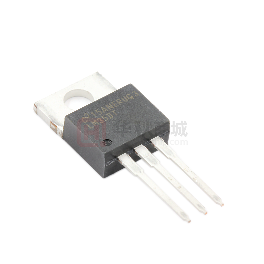
LM35DT
NRND
TO-220
NEB
3
45
Non-RoHS
& Green
Call TI
Level-1-NA-UNLIM
0 to 100
LM35DT
Addendum-Page 1
LM35
CAZ
LM35
CZ
LM35
CZ
Samples
�PACKAGE OPTION ADDENDUM
www.ti.com
30-Sep-2021
Orderable Device
Status
(1)
Package Type Package Pins Package
Drawing
Qty
Eco Plan
(2)
Lead finish/
Ball material
MSL Peak Temp
Op Temp (°C)
Device Marking
(3)
(4/5)
(6)
LM35DT/NOPB
ACTIVE
TO-220
NEB
3
45
RoHS & Green
SN
Level-1-NA-UNLIM
0 to 100
LM35DT
LM35DZ/LFT1
ACTIVE
TO-92
LP
3
2000
RoHS & Green
SN
N / A for Pkg Type
LM35
DZ
LM35DZ/LFT4
ACTIVE
TO-92
LP
3
2000
RoHS & Green
SN
N / A for Pkg Type
LM35
DZ
LM35DZ/NOPB
ACTIVE
TO-92
LP
3
1800
RoHS & Green
SN
N / A for Pkg Type
0 to 100
LM35H
ACTIVE
TO
NDV
3
500
Non-RoHS &
Non-Green
Call TI
Call TI
-55 to 150
( LM35H, LM35H)
LM35H/NOPB
ACTIVE
TO
NDV
3
500
RoHS & Green
Call TI
Level-1-NA-UNLIM
-55 to 150
( LM35H, LM35H)
LM35
DZ
(1)
The marketing status values are defined as follows:
ACTIVE: Product device recommended for new designs.
LIFEBUY: TI has announced that the device will be discontinued, and a lifetime-buy period is in effect.
NRND: Not recommended for new designs. Device is in production to support existing customers, but TI does not recommend using this part in a new design.
PREVIEW: Device has been announced but is not in production. Samples may or may not be available.
OBSOLETE: TI has discontinued the production of the device.
(2)
RoHS: TI defines "RoHS" to mean semiconductor products that are compliant with the current EU RoHS requirements for all 10 RoHS substances, including the requirement that RoHS substance
do not exceed 0.1% by weight in homogeneous materials. Where designed to be soldered at high temperatures, "RoHS" products are suitable for use in specified lead-free processes. TI may
reference these types of products as "Pb-Free".
RoHS Exempt: TI defines "RoHS Exempt" to mean products that contain lead but are compliant with EU RoHS pursuant to a specific EU RoHS exemption.
Green: TI defines "Green" to mean the content of Chlorine (Cl) and Bromine (Br) based flame retardants meet JS709B low halogen requirements of