LM161, LM361
www.ti.com
SNOSBJ5C – MAY 1999 – REVISED MARCH 2013
LM161/LM361 High Speed Differential Comparators
Check for Samples: LM161, LM361
FEATURES
DESCRIPTION
•
•
•
•
•
•
•
•
The LM161/LM361 is a very high speed differential
input, complementary TTL output voltage comparator
with improved characteristics over the SE529/NE529
for which it is a pin-for-pin replacement. The device
has been optimized for greater speed performance
and lower input offset voltage. Typically delay varies
only 3 ns for over-drive variations of 5 mV to 500 mV.
It may be operated from op amp supplies (±15V).
1
2
Independent strobes
Ensured high speed: 20 ns max
Tight delay matching on both outputs
Complementary TTL outputs
Operates from op amp supplies: ±15V
Low speed variation with overdrive variation
Low input offset voltage
Versatile supply voltage range
Complementary outputs having maximum skew are
provided. Applications involve high speed analog to
digital converters and zero-crossing detectors in disk
file systems.
CONNECTION DIAGRAMS
SOIC or PDIP Package
Figure 1. Top View
Package Numbers D0014A, NFF0014A
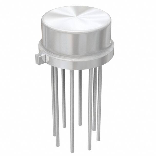
TO-100 Package
Figure 2. Package Number LME0010C
1
2
Please be aware that an important notice concerning availability, standard warranty, and use in critical applications of
Texas Instruments semiconductor products and disclaimers thereto appears at the end of this data sheet.
All trademarks are the property of their respective owners.
PRODUCTION DATA information is current as of publication date.
Products conform to specifications per the terms of the Texas
Instruments standard warranty. Production processing does not
necessarily include testing of all parameters.
Copyright © 1999–2013, Texas Instruments Incorporated
�LM161, LM361
SNOSBJ5C – MAY 1999 – REVISED MARCH 2013
www.ti.com
LOGIC DIAGRAM
*Output is low when current is drawn from strobe pin.
These devices have limited built-in ESD protection. The leads should be shorted together or the device placed in conductive foam
during storage or handling to prevent electrostatic damage to the MOS gates.
Absolute Maximum Ratings
(1)
+
Positive Supply Voltage, V
+16V
Negative Supply Voltage, V−
−16V
Gate Supply Voltage, VCC
+7V
Output Voltage
+7V
Differential Input Voltage
±5V
Input Common Mode Voltage
±6V
Power Dissipation
600 mW
−65°C to +150°C
Storage Temperature Range
Operating Temperature Range
TMIN
TMAX
−55°C to +125°C
LM161
−25°C to +85°C
LM361
0°C to +70°C
Lead Temp. (Soldering, 10 seconds)
260°C
For Any Device Lead Below V−
(1)
0.3V
The device may be damaged by use beyond the maximum ratings.
Operating Conditions
Min
LM161
Supply Voltage V+
Supply Voltage V−
Supply Voltage VCC
ESD Tolerance
(1)
(2)
2
Max
15V
LM361
5V
15V
LM161
−6V
−15V
LM361
−6V
−15V
LM161
4.5V
5V
5.5V
LM361
4.75V
5V
5.25V
(1)
Soldering Information
Typ
5V
1600V
(2)
(2)
PDIP Package
Soldering (10 seconds)
SOIC Package
Vapor Phase (60
seconds)
260°C
215°C
Infrared (15 seconds)
220°C
Human body model, 1.5 kΩ in series with 100 pF.
See AN-450 “Surface Mounting Methods and Their Effect on Product Reliability” for other methods of soldering surface mount devices.
Submit Documentation Feedback
Copyright © 1999–2013, Texas Instruments Incorporated
Product Folder Links: LM161 LM361
�LM161, LM361
www.ti.com
SNOSBJ5C – MAY 1999 – REVISED MARCH 2013
Electrical Characteristics (1) (2) (1)
(V+ = +10V, VCC = +5V, V− = −10V, TMIN ≤ TA ≤ TMAX, unless noted)
Parameter
Conditions
Limits
Units
LM161
Min
Input Offset Voltage
Input Bias Current
LM361
Typ
Max
1
3
Min
5
TA=25°C
Typ
Max
1
5
mV
μA
10
20
μA
30
2
μA
2
Input Offset Current
TA=25°C
Voltage Gain
TA=25°C
3
3
V/mV
Input Resistance
TA=25°C, f=1 kHz
20
20
kΩ
Logical “1” Output Voltage
VCC=4.75V,
ISOURCE=−0.5 mA
3.3
V
Logical “0” Output Voltage
VCC=4.75V,
ISINK=6.4 mA
0.4
0.4
V
Strobe Input “1” Current
(Output Enabled)
VCC=5.25V,
VSTROBE=2.4V
200
200
μA
Strobe Input “0” Current
(Output Disabled)
VCC=5.25V,
VSTROBE=0.4V
−1.6
−1.6
mA
Strobe Input “0” Voltage
VCC=4.75V
0.8
0.8
V
Strobe Input “1” Voltage
VCC=4.75V
Output Short Circuit Current
VCC=5.25V, VOUT=0V
−55
mA
Supply Current I+
V+=10V, V−=−10V,
VCC=5.25V,
−55°C≤TA≤125°C
Supply Current I+
V+=10V, V−=−10V,
VCC=5.25V,
0°C≤TA≤70°C
Supply Current I−
V+=10V, V−=−10V,
VCC=5.25V,
−55°C≤TA≤125°C
Supply Current I−
V+=10V,
V−=−10V,VCC=5.25V,
0°C≤TA≤70°C
Supply Current ICC
V+=10V, V−=−10V,
VCC=5.25V,
−55°C≤TA≤125°C
Supply Current ICC
V+=10V, V−=−10V,
VCC=5.25V,
0°C≤TA≤70°C
Transient Response
VIN = 50 mV overdrive
3
2.4
μA
5
3.3
2.4
2
2
−18
−55
V
−18
4.5
mA
5
10
mA
mA
10
18
mA
mA
20
mA
(3)
Propagation Delay Time (tpd(0))
TA=25°C
14
20
14
20
ns
Propagation Delay Time (tpd(1))
TA=25°C
14
20
14
20
ns
Delay Between Output A and B
TA=25°C
2
5
2
5
ns
Strobe Delay Time (tpd(0))
TA=25°C
8
8
ns
Strobe Delay Time (tpd(1))
TA=25°C
8
8
ns
(1)
Typical thermal impedances are as follows:
(2)
(3)
Refer to RETS161X for LM161H and LM161J military specifications.
Measurements using AC Test circuit, Fanout = 1. The devices are faster at low supply voltages.
Submit Documentation Feedback
Copyright © 1999–2013, Texas Instruments Incorporated
Product Folder Links: LM161 LM361
3
�LM161, LM361
SNOSBJ5C – MAY 1999 – REVISED MARCH 2013
www.ti.com
Typical Performance Characteristics
4
Offset Voltage
Input Currents
vs
Ambient
Temperature
Figure 3.
Figure 4.
Input Characteristics
Supply Current vs
Ambient Temperature
Figure 5.
Figure 6.
Supply Current vs
Supply Voltage
Propagation Delay vs
Ambient Temperature
Figure 7.
Figure 8.
Submit Documentation Feedback
Copyright © 1999–2013, Texas Instruments Incorporated
Product Folder Links: LM161 LM361
�LM161, LM361
www.ti.com
SNOSBJ5C – MAY 1999 – REVISED MARCH 2013
Typical Performance Characteristics (continued)
Delay of Output 1 With
Respect to Output 2 vs
Ambient Temperature
Strobe Delay
vs
Ambient
Temperature
Figure 9.
Figure 10.
Common-Mode
Pulse Response
Propagation Delay vs
Supply Voltage
Figure 11.
Figure 12.
Submit Documentation Feedback
Copyright © 1999–2013, Texas Instruments Incorporated
Product Folder Links: LM161 LM361
5
�LM161, LM361
SNOSBJ5C – MAY 1999 – REVISED MARCH 2013
www.ti.com
AC TEST CIRCUIT
VIN = ±50 mV
+
V = +10V
6
FANOUT = 1
FANOUT = 4
V− = −10V
R = 2.4k
R = 680Ω
VCC = 5.25V
Submit Documentation Feedback
C=15 pF
C = 30 pF
Copyright © 1999–2013, Texas Instruments Incorporated
Product Folder Links: LM161 LM361
�LM161, LM361
www.ti.com
SNOSBJ5C – MAY 1999 – REVISED MARCH 2013
SCHEMATIC DIAGRAM
LM161
R10, R16: 85
R11, R17: 205
Submit Documentation Feedback
Copyright © 1999–2013, Texas Instruments Incorporated
Product Folder Links: LM161 LM361
7
�LM161, LM361
SNOSBJ5C – MAY 1999 – REVISED MARCH 2013
www.ti.com
REVISION HISTORY
Changes from Revision B (March 2013) to Revision C
•
8
Page
Changed layout of National Data Sheet to TI format ............................................................................................................ 7
Submit Documentation Feedback
Copyright © 1999–2013, Texas Instruments Incorporated
Product Folder Links: LM161 LM361
�PACKAGE OPTION ADDENDUM
www.ti.com
4-Aug-2022
PACKAGING INFORMATION
Orderable Device
Status
(1)
Package Type Package Pins Package
Drawing
Qty
Eco Plan
(2)
Lead finish/
Ball material
MSL Peak Temp
Op Temp (°C)
Device Marking
(3)
Samples
(4/5)
(6)
LM361H/NOPB
ACTIVE
TO-100
LME
10
500
RoHS & Green
Call TI
Level-1-NA-UNLIM
0 to 70
( LM361H, LM361H)
Samples
LM361M
ACTIVE
SOIC
D
14
55
Non-RoHS
& Green
Call TI
Level-1-235C-UNLIM
0 to 70
LM361M
Samples
LM361M/NOPB
ACTIVE
SOIC
D
14
55
RoHS & Green
SN
Level-1-260C-UNLIM
0 to 70
LM361M
Samples
LM361MX/NOPB
ACTIVE
SOIC
D
14
2500
RoHS & Green
SN
Level-1-260C-UNLIM
0 to 70
LM361M
Samples
LM361N/NOPB
ACTIVE
PDIP
N
14
25
RoHS & Green
NIPDAU
Level-1-NA-UNLIM
0 to 70
LM361N
Samples
(1)
The marketing status values are defined as follows:
ACTIVE: Product device recommended for new designs.
LIFEBUY: TI has announced that the device will be discontinued, and a lifetime-buy period is in effect.
NRND: Not recommended for new designs. Device is in production to support existing customers, but TI does not recommend using this part in a new design.
PREVIEW: Device has been announced but is not in production. Samples may or may not be available.
OBSOLETE: TI has discontinued the production of the device.
(2)
RoHS: TI defines "RoHS" to mean semiconductor products that are compliant with the current EU RoHS requirements for all 10 RoHS substances, including the requirement that RoHS substance
do not exceed 0.1% by weight in homogeneous materials. Where designed to be soldered at high temperatures, "RoHS" products are suitable for use in specified lead-free processes. TI may
reference these types of products as "Pb-Free".
RoHS Exempt: TI defines "RoHS Exempt" to mean products that contain lead but are compliant with EU RoHS pursuant to a specific EU RoHS exemption.
Green: TI defines "Green" to mean the content of Chlorine (Cl) and Bromine (Br) based flame retardants meet JS709B low halogen requirements of