Sample &
Buy
Product
Folder
Support &
Community
Tools &
Software
Technical
Documents
LM3668
SNVS449O – JUNE 2007 – REVISED APRIL 2015
LM3668 1-A, High-Efficiency Dual-Mode Single-Inductor Buck-Boost DC-DC Converter
1 Features
2 Applications
•
•
•
•
•
•
•
•
1
•
•
•
•
•
•
•
•
•
45-µA Typical Quiescent Current
For 2.8-V-3.3-V and 3-V-3.4-V Versions:
– 1-A Maximum Load Current for
VIN = 2.8 V to 5.5 V
– 800-mA Maximum Load Current for
VIN = 2.7 V
– 600-mA Maximum Load Current for
VIN = 2.5 V
For 4.5 V-5 V
– 1-A Maximum Load Current for
VIN = 3.9 V to 5.5 V
– 800-mA Maximum Load Current for
VIN = 3.4 V to 3.8 V
– 700-mA Maximum Load Current for
VIN = 3 V to 3.3 V
– 600-mA Maximum Load Current for
VIN = 2.7 V to 2.9 V
2.2-MHz PWM Fixed Switching Frequency
(Typical)
Automatic PFM-PWM Mode or Forced PWM
Mode
Wide Input Voltage Range: 2.5 V to 5.5 V
Internal Synchronous Rectification for High
Efficiency
Internal Soft Start: 600-µs Maximum Start-Up
Time After VIN Settled
0.01-µA Typical Shutdown Current
Current Overload and Thermal Shutdown
Protection
Frequency Sync Pin: 1.6 MHz to 2.7 MHz
Typical Application Circuit
VIN = 2.5V - 5.5V
C1
10 PF
VDD
PVIN
LM3668
SW2
The LM3668 is a synchronous buck-boost DC-DC
converter optimized for powering low voltage circuits
from a Li-Ion battery and input voltage rails between
2.5 V and 5.5 V. It has the capability to support up to
1-A output current over the output voltage range. The
LM3668 regulates the output voltage over the
complete input voltage range by automatically
switching between buck or boost modes depending
on the input voltage.
The LM3668 has 2 N-channel MOSFETS and 2 Pchannel MOSFETS arranged in a topology that
provides continuous operation through the buck and
boost operating modes. There is a MODE pin that
allows the user to choose between an intelligent
automatic PFM-PWM mode operation and forced
PWM operation. During PWM mode, a fixedfrequency 2.2 MHz (typical) is used. PWM mode
drives load up to 1 A. Hysteretic PFM mode extends
the battery life through reduction of the quiescent
current to 45 µA (typical) at light loads during system
standby. Internal synchronous rectification provides
high efficiency. In shutdown mode (EN pin pulled
low), the device turns off and reduces battery
consumption to 0.01 µA (typical).
A high switching frequency of 2.2 MHz (typical)
allows the use of tiny surface-mount components
including a 2.2-µH inductor, a 10-µF input capacitor,
and a 22-µF output capacitor.
Device Information(1)
PART NUMBER
LM3668
FB
C2
22 PF
SYNC/MODE
EN
NC SGND
3 Description
2.8V/3.3V
VOUT
SW1
2.2 PH
Handset Peripherals
MP3 Players
Pre-Regulation for Linear Regulators
PDAs
Portable Hard Disk Drives
WiMax Modems
VSEL
PGND
L = 2.8V
H = 3.3V
PACKAGE
BODY SIZE (NOM)
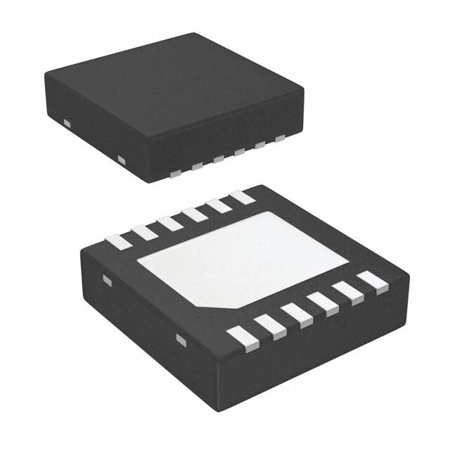
WSON (12)
3.00 mm x 3.00 mm
(1) For all available packages, see the orderable addendum at
the end of the datasheet.
1
An IMPORTANT NOTICE at the end of this data sheet addresses availability, warranty, changes, use in safety-critical applications,
intellectual property matters and other important disclaimers. PRODUCTION DATA.
�LM3668
SNVS449O – JUNE 2007 – REVISED APRIL 2015
www.ti.com
Table of Contents
1
2
3
4
5
6
7
8
Features ..................................................................
Applications ...........................................................
Description .............................................................
Revision History.....................................................
Device Comparison Table.....................................
Pin Configuration and Functions .........................
Specifications.........................................................
1
1
1
2
3
3
4
7.1
7.2
7.3
7.4
7.5
7.6
4
4
4
5
5
6
Absolute Maximum Ratings ......................................
ESD Ratings..............................................................
Recommended Operating Conditions.......................
Thermal Information ..................................................
Electrical Characteristics...........................................
Typical Characteristics ..............................................
Detailed Description ............................................ 13
8.1 Overview ................................................................. 13
8.2 Functional Block Diagram ....................................... 14
8.3 Feature Description................................................. 14
8.4 Device Functional Modes........................................ 16
9
Application and Implementation ........................ 19
9.1 Application Information............................................ 19
9.2 Typical Application .................................................. 19
10 Power Supply Recommendations ..................... 23
11 Layout................................................................... 23
11.1 Layout Guidelines ................................................. 23
11.2 Layout Example .................................................... 23
12 Device and Documentation Support ................. 24
12.1
12.2
12.3
12.4
Device Support......................................................
Trademarks ...........................................................
Electrostatic Discharge Caution ............................
Glossary ................................................................
24
24
24
24
13 Mechanical, Packaging, and Orderable
Information ........................................................... 24
4 Revision History
NOTE: Page numbers for previous revisions may differ from page numbers in the current version.
Changes from Revision N (August 2014) to Revision O
•
Changed RθJA value from 34 to 47.3; change 20 PINS to 12 PINS in header; add additional thermal information............... 5
Changes from Revision M (May 2013) to Revision N
•
2
Page
Added Pin Configuration and Functions section, Handling Rating table, Feature Description section, Device
Functional Modes, Application and Implementation section, Power Supply Recommendations section, Layout
section, Device and Documentation Support section, and Mechanical, Packaging, and Orderable Information
section ................................................................................................................................................................................... 1
Changes from Revision L (April 2013) to Revision M
•
Page
Page
Changed layout of National Data Sheet to TI format ........................................................................................................... 23
Submit Documentation Feedback
Copyright © 2007–2015, Texas Instruments Incorporated
Product Folder Links: LM3668
�LM3668
www.ti.com
SNVS449O – JUNE 2007 – REVISED APRIL 2015
5 Device Comparison Table
OUTPUT VOLTAGE
(V)
ORDER NUMBER
LM3668SD-2833/NOPB
LM3668SDX-2833/NOPB
LM3668SD-3034/NOPB
LM3668SDX-3034/NOPB
LM3668SD-4550/NOPB
PACKAGE
PACKAGE MARKING
SUPPLIED AS
2.8, VSEL = low
3.3, VSEL = high
S017B
1000 units, tape-and-reel
3, VSEL = low
3.4, VSEL = high
S018B
4500 units, tape-and-reel
DQB (WSON)
4500 units, tape-and-reel
4.5, VSEL = low
5, VSEL = high
LM3668SDX-4550/NOPB
1000 units, tape-and-reel
S019B
1000 units, tape-and-reel
4500 units, tape-and-reel
6 Pin Configuration and Functions
DQB Package
12-Pin WSON
Top View
VOUT
SW2
DQB Package
12-Pin WSON
Bottom View
1
2
12
FB
11
VSEL
10
MODE/
SYNC
3
PGND
DAP
SW1
4
9
SGND
PVIN
5
8
NC
EN
6
7
VDD
FB
12
1
VOUT
VSEL
11
2
SW2
MODE/
SYNC
10
3
PGND
SGND
9
4
SW1
NC
8
5
PVIN
VDD
7
6
EN
DAP
Pin Functions (1)
PIN
(1)
TYPE
DESCRIPTION
NO.
NAME
1
VOUT
A
Connect to output capacitor.
2
SW2
A
Switching node connection to the internal PFET switch (P2) and NFET synchronous
rectifier (N2).
3
PGND
G
Power ground.
4
SW1
A
Switching node connection to the internal PFET switch (P1) and NFET synchronous
rectifier (N1).
5
PVIN
P
Supply to the power switch, connect to the input capacitor.
6
EN
I
Enable input. Set this digital input high for normal operation. For shutdown, set low.
7
VDD
P
Signal supply input. If board layout is not optimum an optional 1-µF ceramic capacitor
is suggested as close to this pin as possible.
8
NC
-
No connect. Connect this pin to SGND on PCB layout.
9
SGND
G
Analog and Control Ground.
10
MODE/SYNC
I
Mode = LOW, Automatic Mode. Mode= HI, forced PWM Mode. SYNC = external clock
synchronization from 1.6 MHz to 2.7 MHz.(When SYNC function is used, device is
forced in PWM mode).
11
VSEL
I
Voltage selection pin; (for example, 2.8-V-3.3-V option) logic input low (or GND) = 2.8
V and logic high = 3.3 V (or VIN) to set output voltage.
12
FB
A
Feedback analog input. Connect to the output at the output filter.
DAP
DAP
-
Die Attach Pad, connect the DAP to SGND on PCB layout to enhance thermal
performance. It should not be used as a primary ground connection.
A: Analog Pin, G: Ground Pin, P: Power Pin, I: Digital Input Pin
Submit Documentation Feedback
Copyright © 2007–2015, Texas Instruments Incorporated
Product Folder Links: LM3668
3
�LM3668
SNVS449O – JUNE 2007 – REVISED APRIL 2015
www.ti.com
7 Specifications
7.1 Absolute Maximum Ratings
over operating free-air temperature range (unless otherwise noted) (1) (2)
MIN
MAX
UNIT
–0.2
6
V
(PGND and SGND-0.2)
(PVIN + 0.2)
V
–0.2
0.2
V
Maximum junction temperature (TJ-MAX)
125
°C
Maximum lead temperature (soldering, 10 sec)
260
°C
150
°C
PVIN, VDD, SW1, SW2 & VOUT pins: voltage to SGND & PGND
FB, EN, and MODE/SYNC pins
PGND to SGND
Continuous power dissipation (3)
Internally Limited
Storage temperature , Tstg
(1)
(2)
(3)
–65
Stresses beyond those listed under Absolute Maximum Ratings may cause permanent damage to the device. These are stress ratings
only, which do not imply functional operation of the device at these or any other conditions beyond those indicated under Recommended
Operating Conditions. Exposure to absolute-maximum-rated conditions for extended periods may affect device reliability.
If Military/Aerospace specified devices are required, please contact the Texas Instruments Sales Office/Distributors for availability and
specifications.
In applications where high power dissipation and/or poor package thermal resistance is present, the maximum ambient temperature may
have to be derated. Maximum ambient temperature (TA-MAX) is dependent on the maximum operating junction temperature (TJ-MAX-OP =
125ºC), the maximum power dissipation of the device in the application (PD-MAX), and the junction-to ambient thermal resistance of the
part/package in the application (RθJA), as given by the following equation: TA-MAX = TJ-MAX-OP – (RθJA × PD-MAX).
7.2 ESD Ratings
VALUE
Human-body model (HBM), per ANSI/ESDA/JEDEC JS-001
V(ESD)
(1)
(2)
Electrostatic discharge
(1)
UNIT
±2500
Charged-device model (CDM), per JEDEC specification JESD22C101 (2)
V
±1250
JEDEC document JEP155 states that 500-V HBM allows safe manufacturing with a standard ESD control process.
JEDEC document JEP157 states that 250-V CDM allows safe manufacturing with a standard ESD control process.
7.3 Recommended Operating Conditions
Input voltage
Recommended load current
Junction temperature (TJ)
Ambient temperature (TA)
(1)
4
(1)
MIN
MAX
2.5
5.5
UNIT
V
0
1
A
−40
125
°C
−40
85
°C
In applications where high power dissipation and/or poor package thermal resistance is present, the maximum ambient temperature may
have to be derated. Maximum ambient temperature (TA-MAX) is dependent on the maximum operating junction temperature (TJ-MAX-OP =
125ºC), the maximum power dissipation of the device in the application (PD-MAX), and the junction-to ambient thermal resistance of the
part/package in the application (RθJA), as given by the following equation: TA-MAX = TJ-MAX-OP – (RθJA × PD-MAX).
Submit Documentation Feedback
Copyright © 2007–2015, Texas Instruments Incorporated
Product Folder Links: LM3668
�LM3668
www.ti.com
SNVS449O – JUNE 2007 – REVISED APRIL 2015
7.4 Thermal Information
LM3668
THERMAL METRIC (1)
DQB (WSON)
UNIT
12 PINS
RθJA
Junction-to-ambient thermal resistance, WSON package (2)
47.3
RθJC(top)
Junction-to-case (top) thermal resistance
43..4
RθJB
Junction-to-board thermal resistance
21.6
ψJT
Junction-to-top characterization parameter
0.4
ψJB
Junction-to-board characterization parameter
21.7
RθJC(bot)
Junction-to-case (bottom) thermal resistance
3.5
(1)
(2)
°C/W
For more information about traditional and new thermal metrics, see the IC Package Thermal Metrics application report, SPRA953.
Junction-to-ambient thermal resistance (RθJA) is taken from a thermal modeling result, performed under the conditions and guidelines
set forth in the JEDEC standard JESD51-7. The test board is a 4-layer FR-4 board measuring 101.6 mm x 76.2 mm x 1.6 mm.
Thickness of the copper layers are 2oz/1oz/1oz/2oz. The middle layer of the board is 60 mm x 60 mm. Ambient temperature in
simulation is 22°C, still air. Junction-to-ambient thermal resistance is highly application and board-layout dependent. In applications
where high maximum power dissipation exists, special care must be paid to thermal dissipation issues in board design.
7.5 Electrical Characteristics
Unless otherwise noted, specifications apply to the LM3668. VIN = 3.6 V = EN, VOUT = 3.3 V. For VOUT = 4.5V-5 V, VIN =
4 V. (1) (2)
PARAMETER
TEST CONDITIONS
MIN
TYP
MAX
UNIT
Feedback voltage
−40°C ≤ TA ≤ 85°C, see (2)
Switch peak current limit
Open loop (3)
Switch peak current limit
(3)
Open loop , −40°C ≤ TA ≤ 85°C
Shutdown supply current
EN = 0 V
Shutdown supply current
EN = 0 V, −40°C ≤ TA ≤ 85°C
DC bias current in PFM
No load, device is not switching (FB
forced higher than programmed output
voltage)
DC bias current in PFM
No load, device is not switching (FB
forced higher than programmed output
voltage)
−40°C ≤ TA ≤ 85°C
DC bias current in PWM
PWM mode, no switching
DC bias current in PWM
PWM mode, no switching
−40°C ≤ TA ≤ 85°C
RDSON(P)
Pin-pin resistance for PFET
Switches P1 and P2
130
180
mΩ
RDSON(N)
Pin-pin resistance for NFET
Switches N1 and N2
100
150
mΩ
PWM mode
2.2
VFB
ILIM
ISHDN
IQ_PFM
IQ_PWM
FOSC
Internal oscillator frequency
FSYNC
–3%
3%
1.85
1.6
2.05
0.01
1
µA
60
600
750
1.9
2.5
Sync frequency range
VIN = 3.6 V
1.6
2.7
VIH
Logic high input for EN,
MODE/SYNC pins
−40°C ≤ TA ≤ 85°C
1.1
VIL
Logic low input for EN,
MODE/SYNC pins
−40°C ≤ TA ≤ 85°C
IEN, MODE,
EN, MODE/SYNC pins input current
(1)
(2)
(3)
µA
MHz
MHz
V
0.4
0.3
−40°C ≤ TA ≤ 85°C
µA
45
PWM mode, −40°C ≤ TA ≤ 85°C
SYNC
A
1
V
µA
All voltages with respect to SGND.
Minimum and Maximum limits are specified by design, test, or statistical analysis. Typical numbers are not ensured, but do represent the
most likely norm.
Electrical Characteristics table reflects open loop data (FB = 0 V and current drawn from SW pin ramped up until cycle-by-cycle current
limits is activated). Closed loop current limit is the peak inductor current measured in the application circuit by increasing output current
until output voltage drops by 10%.
Submit Documentation Feedback
Copyright © 2007–2015, Texas Instruments Incorporated
Product Folder Links: LM3668
5
�LM3668
SNVS449O – JUNE 2007 – REVISED APRIL 2015
www.ti.com
7.6 Typical Characteristics
Typical Application Circuit (see Figure 46): VIN = 3.6 V, L = 2.2 µH, CIN = 10 µF, COUT = 22 µF (4), TA = 25°C , unless otherwise
stated.
900
2.4
VIN = 2.5V
IQ_5.5V
800
2.3
IQ_PWM (éA)
FREQUENCY (MHz)
IQ_3.6V
700
600
500
400
IQ_2.5V
2.2
VIN = 3.6V
2.1
VIN = 5.5V
2.0
300
200
-40
-20
0
20
40
60
80
1.9
-40
100
-20
0
TEMPERATURE (°C)
Figure 1. Supply Current vs Temperature (Not Switching)
(VOUT = 3.4 V)
40
60
80
100
Figure 2. Switching Frequency vs. Temperature
(VOUT = 3.4 V)
150
200
NFET = 2.5V
PFET_RDS = 2.5V PFET_RDS = 2.7V
NFET = 2.7V
175
RESISTANCE (mÖ)
125
RESISTANCE (mÖ)
20
TEMPERATURE (°C)
100
75
NFET = 5.5V
50
NFET = 3.6V
150
125
100
75
PFET_RDS = 3.6V
50
PFET_RDS = 5.5V
25
0
-40
25
-20
0
20
40
60
80
0
-40
100
-20
0
TEMPERATURE (°C)
20
40
60
80
100
TEMPERATURE (°C)
Figure 3. NFET_RDS (on) vs. Temperature (VOUT = 3.4 V)
Figure 4. PFET_RDS (on) vs. Temperature (VOUT = 3.4 V)
2.00
100
90
1.95
EFFICIENCY (%)
80
ILIMIT (A)
1.90
VIN = 3.6V
1.85
1.80
VIN = 2.5V
70
60
VIN = 2.7V
50
40
30
VIN = 5.0V
20
1.75
VIN = 5.5V
10
1.70
-40
-20
0
20
40
60
80
0
0
100
TEMPERATURE (°C)
6
1
10
100
1000
LOAD (mA)
Figure 5. ILIMIT vs. Temperature (VOUT = 3.4 V)
(4)
VIN = 3.6V
Figure 6. Efficiency at VOUT = 2.8 V (Forced PWM Mode)
CIN and COUT: Low-ESR Surface-Mount Ceramic Capacitors (MLCCs) used in setting electrical characteristics. COUT_MIN should not
exceed −40% of suggested value. The preferable choice would be a type and make MLCC that issues –30% over the operating
temperature and voltage range.
Submit Documentation Feedback
Copyright © 2007–2015, Texas Instruments Incorporated
Product Folder Links: LM3668
�LM3668
www.ti.com
SNVS449O – JUNE 2007 – REVISED APRIL 2015
Typical Characteristics (continued)
Typical Application Circuit (see Figure 46): VIN = 3.6 V, L = 2.2 µH, CIN = 10 µF, COUT = 22 µF(4), TA = 25°C , unless otherwise
stated.
100
100
90
90
80
VIN = 2.5V
70
60
50
40
EFFICIENCY (%)
EFFICIENCY (%)
80
VIN = 2.7V
VIN = 3.6V
VIN = 5.0V
30
20
VIN = 5.5V
VIN = 2.5V
60
VIN = 2.7V
50
VIN = 5.5V
40
30
VIN = 5.0V
20
10
0
0
70
10
1
10
100
0
0
1000
VIN = 3.6V
1
10
LOAD (mA)
100
1000
LOAD (mA)
Figure 7. Efficiency at VOUT = 2.8 V (Auto Mode)
Figure 8. Efficiency at VOUT = 3 V (Forced PWM Mode)
100
90
EFFICIENCY (%)
80
VIN = 2.5V
70
60
VIN = 2.7V
VIN = 3.3V
50
40
30
VIN = 3.6V
20
10
0
0
VIN = 5.5V
1
10
100
1000
LOAD (mA)
Figure 9. Efficiency at VOUT = 3 V (Auto Mode)
Figure 10. Efficiency at VOUT = 3.3 V (Forced PWM Mode)
100
100
90
90
80
VIN = 2.5V
70
60
EFFICIENCY (%)
EFFICIENCY (%)
80
VIN = 2.7V
VIN = 3.3V
50
40
VIN = 3.6V
30 VIN = 5.5V
20
60
VIN = 2.7V
50
40
30
VIN = 5.0V
20
10
0
0
VIN = 2.5V
70
VIN = 5.5V
10
1
10
100
0
0
1000
LOAD (mA)
VIN = 3.6V
1
10
100
1000
LOAD (mA)
Figure 11. Efficiency at VOUT = 3.3 V (Auto Mode)
Figure 12. Efficiency at VOUT = 3.4 V (Forced PWM Mode)
Submit Documentation Feedback
Copyright © 2007–2015, Texas Instruments Incorporated
Product Folder Links: LM3668
7
�LM3668
SNVS449O – JUNE 2007 – REVISED APRIL 2015
www.ti.com
Typical Characteristics (continued)
Typical Application Circuit (see Figure 46): VIN = 3.6 V, L = 2.2 µH, CIN = 10 µF, COUT = 22 µF(4), TA = 25°C , unless otherwise
stated.
100
100
90
90
80
VIN = 2.5V
70
VIN = 5.0V
60
50
VIN = 2.7V
VIN = 3.6V
40
30
70
EFFICIENCY (%)
EFFICIENCY (%)
80
VIN = 5.5V
60
40
30
20
10
10
1
10
100
VIN = 2.7V
VIN = 3.6V
50
20
0
0
VIN = 5V
0
0
1000
VIN = 5.5V
1
LOAD (mA)
100
100
90
90
80
80
70
70
VIN = 5.5V
VIN = 2.7V
50
40
VIN = 3.6V
VIN = 5.0V
30
30
10
100
0
0
1000
LOAD (mA)
VIN = 2.7V
40
20
10
VIN = 3.6V
50
10
1
1000
VIN = 5.5V
60
20
0
0
100
Figure 14. Efficiency at VOUT = 4.5 V (Forced PWM Mode)
EFFICIENCY (%)
EFFICIENCY (%)
Figure 13. Efficiency at VOUT = 3.4 V (Auto Mode)
60
10
LOAD (mA)
VIN = 5.0V
1
10
100
1000
LOAD (mA)
Figure 15. Efficiency at VOUT = 4.5 V (Auto Mode)
Figure 16. Efficiency at VOUT = 5 V (Forced PWM Mode)
100
90
4.5V
EFFICIENCY (%)
80
VIN
3.7V
70
VIN =5.0V
VIN = 3.6V
60
50
VOUT_AC
100 mV/DIV
40
30
VIN = 5.5V
VIN = 2.7V
5V/DIV
SW2
5V/DIV
SW1
20
10
0
0
1
10
100
1000
LOAD (mA)
100 Ps/DIV
Figure 17. Efficiency at VOUT = 5 V (Auto Mode)
8
Figure 18. Line Transient in Buck Mode (VOUT = 3.4 V, Load
= 500 mA)
Submit Documentation Feedback
Copyright © 2007–2015, Texas Instruments Incorporated
Product Folder Links: LM3668
�LM3668
www.ti.com
SNVS449O – JUNE 2007 – REVISED APRIL 2015
Typical Characteristics (continued)
Typical Application Circuit (see Figure 46): VIN = 3.6 V, L = 2.2 µH, CIN = 10 µF, COUT = 22 µF(4), TA = 25°C , unless otherwise
stated.
3.4V
VIN
2.8V
4.0V
3.4V
100 mV/DIV
VOUT_AC
5V/DIV
5V/DIV
VIN
VOUT_AC
100 mV/DIV
SW2
5V/DIV
SW2
SW1
5V/DIV
SW1
100 Ps/DIV
100 Ps/DIV
Figure 19. Line Transient in Boost Mode (VOUT = 3.4 V, Load
= 500 mA)
Figure 20. Line Transient in Buck-Boost Mode (VOUT = 3.4 V,
Load = 500 mA)
SW2
5V/DIV
SW2
5V/DIV
5V/DIV
SW1
200
mv/DIV
VOUT_AC
5V/DIV
SW1
200 mV/DIV
VOUT_AC
500
mA/DIV
LOAD
LOAD
500 mA/DIV
100 Ps/DIV
100 Ps/DIV
Figure 21. Load Transient in Buck Mode (Forced PWM
Mode) VIN = 4.2 V, VOUT = 3.4 V, Load = 0 to 500 mA
Figure 23. Load Transient in Buck-Boost Operation (Forced
PWM Mode) VIN = 3.44 V, VOUT = 3.4 V, Load = 0 to 500 mA
Figure 22. Load Transient in Boost Operation (Forced PWM
Mode) VIN = 2.7 V, VOUT = 3.4 V, Load = 0 to 500 mA
Figure 24. Load Transient in Buck Mode (Forced PWM
Mode) VIN = 4.2 V, VOUT = 3 V, Load = 0 to 500 mA
Submit Documentation Feedback
Copyright © 2007–2015, Texas Instruments Incorporated
Product Folder Links: LM3668
9
�LM3668
SNVS449O – JUNE 2007 – REVISED APRIL 2015
www.ti.com
Typical Characteristics (continued)
Typical Application Circuit (see Figure 46): VIN = 3.6 V, L = 2.2 µH, CIN = 10 µF, COUT = 22 µF(4), TA = 25°C , unless otherwise
stated.
10
Figure 25. Load Transient in Boost Mode (Forced PWM
Mode) VIN = 2.7 V, VOUT = 3 V, Load = 0 to 500 mA
Figure 26. Load Transient in Buck-Boost Mode (Forced
PWM Mode) VIN = 3.05 V, VOUT = 3 V, Load = 0 to 500 mA
Figure 27. Load Transient in Buck Mode (Auto Mode) VIN =
4.2 V, VOUT = 3.3 V, Load = 50 to 150 mA
Figure 28. Load Transient in Boost Mode (Auto Mode) VIN =
2.7 V, VOUT = 3.3 V, Load = 50 to 150 mA
Figure 29. Load Transient in Buck-Boost Mode (Auto Mode)
VIN = 3.6 V, VOUT = 3.3 V, Load = 50-150 mA
Figure 30. Load Transient in Buck Mode (Forced PWM
Mode) VIN = 5.5 V, VOUT = 5 V, Load = 0 to 500 mA
Submit Documentation Feedback
Copyright © 2007–2015, Texas Instruments Incorporated
Product Folder Links: LM3668
�LM3668
www.ti.com
SNVS449O – JUNE 2007 – REVISED APRIL 2015
Typical Characteristics (continued)
Typical Application Circuit (see Figure 46): VIN = 3.6 V, L = 2.2 µH, CIN = 10 µF, COUT = 22 µF(4), TA = 25°C , unless otherwise
stated.
Figure 31. Load Transient in Boost Mode (Forced PWM
Mode) VIN = 3.5 V, VOUT = 5 V, Load = 0 to 500 mA
Figure 32. Typical Switching Waveform in Boost Mode
(PWM Mode) VIN = 2.7 V, VOUT = 3 V, Load = 500 mA
2V/DIV
SW2
2V/DIV
SW1
50
mv/DIV
VOUT_AC
500
mA/DIV
Figure 33. Typical Switching Waveform in Buck Mode (PWM
Mode) VIN = 3.6 V, VOUT = 3 V, Load = 500 mA
LOAD
5 Ps/DIV
Figure 34. Typical Switching Waveformt in Boost Mode
(PFM Mode) VIN = 2.7 V, VOUT = 3 V, Load = 50 mA
SW2
5V/DIV
5V/DIV
SW1
5V/DIV
SW2
5V/DIV
SW1
50
mv/DIV
VOUT_AC
500
mA/DIV
LOAD
VOUT_AC
50
mv/DIV
500
mA/DIV
LOAD
200 ns/DIV
5 Ps/DIV
Figure 35. Typical Switching Waveform in Buck Mode (PFM
Mode) VIN = 3.6 V, VOUT = 3 V, Load = 50mA
Figure 36. Typical Switching Waveform in Boost Mode
(PWM Mode) VIN = 3 V, VOUT = 3.4 V, Load = 500 mA
Submit Documentation Feedback
Copyright © 2007–2015, Texas Instruments Incorporated
Product Folder Links: LM3668
11
�LM3668
SNVS449O – JUNE 2007 – REVISED APRIL 2015
www.ti.com
Typical Characteristics (continued)
Typical Application Circuit (see Figure 46): VIN = 3.6 V, L = 2.2 µH, CIN = 10 µF, COUT = 22 µF(4), TA = 25°C , unless otherwise
stated.
2V/DIV
SW2
2V/DIV
SW1
50
mv/DIV
VOUT_AC
500
mA/DIV
LOAD
500 Ps/DIV
Figure 37. Typical Switching Waveform in Buck Mode (PWM
Mode) VIN = 4 V, VOUT = 3.4 V, Load = 500 mA
Figure 38. Typical Switching Waveform in Boost Mode (PFM
Mode) VIN = 3 V, VOUT = 3.4 V, Load = 50 mA
5V/DIV
SW2
5V/DIV
SW1
50
mv/DIV
VOUT_AC
500
mA/DIV
LOAD
500 Ps/DIV
Figure 39. Typical Switching Waveform in Buck Mode (PFM Mode) VIN = 4 V, VOUT = 3.4 V, Load = 50 mA
12
Submit Documentation Feedback
Copyright © 2007–2015, Texas Instruments Incorporated
Product Folder Links: LM3668
�LM3668
www.ti.com
SNVS449O – JUNE 2007 – REVISED APRIL 2015
8 Detailed Description
8.1 Overview
The LM3668, a high-efficiency buck or boost DC-DC converter, delivers a constant voltage from either a single
Li-Ion or three cell NIMH/NiCd battery to portable devices such as mobile phones and PDAs. Using a voltage
mode architecture with synchronous rectification, the device has the ability to deliver up to 1 A, depending on the
input voltage, output voltage, ambient temperature and the chosen inductor.
In addition, the device incorporates a seamless transition from buck-to-boost or boost-to-buck mode. The internal
error amplifier continuously monitors the output to determine the transition from buck-to-boost or boost-to-buck
operation. Figure 40 shows the four switches network used for the buck and boost operation. Table 1
summarizes the state of the switches in different modes.
There are three modes of operation depending on the current required: Pulse Width Modulation (PWM), Pulse
Frequency Modulation (PFM), and shutdown. The device operates in PWM mode at load currents of
approximately 80 mA or higher to improve efficiency. Lighter load current causes the device to automatically
switch into PFM mode to reduce current consumption and extend battery life. Shutdown mode turns off the
device, offering the lowest current consumption.
VIN
VOUT
P1
P2
SW1
SW2
N1
N2
Figure 40. Simplified Diagram of Switches
Table 1. State of Switches in Different Modes
MODE
ALWAYS ON
ALWAYS OFF
SWITCHING
Buck
SW P2
SW N2
SW P1 & N1
Boost
SW P1
SW N1
SW N2 & P2
Submit Documentation Feedback
Copyright © 2007–2015, Texas Instruments Incorporated
Product Folder Links: LM3668
13
�LM3668
SNVS449O – JUNE 2007 – REVISED APRIL 2015
www.ti.com
8.2 Functional Block Diagram
Sw1
Sw2
P2
P1
PVIN
VOUT
Switch
buffer
N2
N1
Switch
buffer
NC
VDD
Control Logic
PFM_hi
PFM
Generator
PFM_low
SYNC/
MODE
FB
Buffer
2 MHz
Oscillator
EN
VSEL
Error
Amp
PWM
Comparator
+
-
Ramp
Generator
VREF
Soft
Start
PGND
SGND
8.3 Feature Description
8.3.1 Buck Operation
When the input voltage is greater than the output voltage, the device operates in buck mode where switch P2 is
always ON and P1 and N1 control the output. Figure 41 shows the simplified circuit for buck mode operation.
P1
SW2
SW1
P2
VIN
+
-
N1
Load
Figure 41. Simplified Circuit for Buck Operation
8.3.2 Boost Operation
When the input voltage is smaller than the output voltage, the device enters boost mode operation where P1 is
always ON, while switches N2 and P2 control the output. Figure 42 shows the simplified circuit for boost mode
operation.
14
Submit Documentation Feedback
Copyright © 2007–2015, Texas Instruments Incorporated
Product Folder Links: LM3668
�LM3668
www.ti.com
SNVS449O – JUNE 2007 – REVISED APRIL 2015
Feature Description (continued)
P1
SW1
SW2
P2
VIN
+
-
N2
Load
Figure 42. Simplified Circuit for Boost Operation
8.3.3 Internal Synchronous Rectification
While in PWM mode, the LM3668 uses an internal MOSFET as a synchronous rectifier to reduce rectifier forward
voltage drop and associated power loss. Synchronous rectification provides a significant improvement in
efficiency whenever the output voltage is relatively low compare to the voltage drop across an ordinary rectifier
diode.
8.3.4 Current Limit Protection
The LM3668 has current limit protection to prevent excessive stress on itself and external components during
overload conditions. The internal current limit comparator will disable the power device at a typical switch peak
current limit of 1.85 A (typ.).
8.3.5 Undervoltage Protection
The LM3668 has an UVP comparator to turn the power device off in case the input voltage or battery voltage is
too low . The typical UVP threshold is around 2 V.
8.3.6 Short Circuit Protection
When the output of the LM3668 is shorted to GND, the current limit is reduced to about half of the typical current
limit value until the short is removed.
8.3.7 Shutdown
When the EN pin is pulled low, P1 and P2 are off; N1 and N2 are turned on to pull SW1 and SW2 to ground.
8.3.8
Thermal Shutdown
The LM3668 has an internal thermal shutdown function to protect the die from excessive temperatures. The
thermal shutdown trip point is typically 150°C; normal operation resumes when the temperature drops below
125°C.
8.3.9 Start-Up
The LM3668 has a soft-start circuit that smooth the output voltage and ramp current during start-up. During startup the bandgap reference is slowly ramped up and switch current limit is reduced to half the typical value. Soft
start is activated only if EN goes from logic low to logic high after VIN reaches 2.5 V. The start-up time thereby
depends on the output capacitor and load current demanded at start-up. It is not recommended to start up the
device at full load while in soft-start.
Submit Documentation Feedback
Copyright © 2007–2015, Texas Instruments Incorporated
Product Folder Links: LM3668
15
�LM3668
SNVS449O – JUNE 2007 – REVISED APRIL 2015
www.ti.com
8.4 Device Functional Modes
8.4.1 PWM Operation
In PWM operation, the output voltage is regulated by switching at a constant frequency and then modulating the
energy per cycle to control power to the load. In Normal operation, the internal error amplifier provides an error
signal, Vc, from the feedback voltage and Vref. The error amplifier signal, Vc, is compared with a voltage,
Vcenter, and used to generate the PWM signals for both buck & boost modes. Signal Vcenter is a DC signal
which sets the transition point of the buck and boost modes. Below are three regions of operation:
• Region I: If Vc is less than Vcenter, Buck mode.
• Region II: If Vc and Vcenter are equal, both PMOS switches (P1, P2) are on and both NMOS switches (N1,
N2) are off. The power passes directly from input to output via P1 & P2
• Region III: If Vc is greater than Vcenter, Boost mode.
The Buck-Boost operation is avoided, to improve the efficiency across VIN and load range.
Vcenter
Vc
PWM
Generator
+
-
+
P1b_PWM
+
P2b_PWM
VOS
Vramp
Figure 43. PWM Generator Block Diagram
8.4.2 PFM Operation
At very light loads, the converter enters PFM mode and operates with reduced switching frequency and supply
current to maintain high efficiency. The part automatically transitions into PFM mode when either of two following
conditions occur for a duration of 128 or more clock cycles:
A. The inductor current reaches zero.
B. The peak inductor current drops below the IMODE level, (Typically IMODE < 45 mA + VIN/80 Ω ).
In PFM operation, the compensation circuit in the error amplifier is turned off. The error amplifier works as a
hysteretic comparator. The PFM comparator senses the output voltage via the feedback pin and controls the
switching of the output FETs such that the output voltage ramps between ~0.8% and ~1.6% of the nominal PWM
output voltage (Figure 44). If the output voltage is below the ‘high’ PFM comparator threshold, the P1 & P2 (Buck
mode) or N2 & P1 (Boost mode) power switches are turned on. It remains on until the output voltage reaches the
‘high’ PFM threshold or the peak current exceeds the IPFM level set for PFM mode. The typical peak current in
PFM mode is: IPFM = 220 mA
Once the P1 (Buck mode) or N2 (Boost mode) power switch is turned off, the N1 & P2 (Buck mode) or P1 & P2
(Boost mode) power switches are turned on until the inductor current ramps to zero. When the zero inductor
current condition is detected, the N1(Buck mode) or P2 (Boost mode) power switches are turned off. If the output
voltage is below the ‘high’ PFM comparator threshold, the P1 & P2 (Buck mode) or N2 & P1 (Boost mode)
switches are again turned on and the cycle is repeated until the output reaches the desired level. Once the
output reaches the ‘high’ PFM threshold, the N1 & P2 (Buck mode) or P1 & P2 (Boost mode) switches are turned
on briefly to ramp the inductor current to zero, then both output switches are turned off and the part enters an
extremely low power mode. Quiescent supply current during this ‘sleep’ mode is 45 µA (typ), which allows the
part to achieve high efficiency under extremely light load conditions.
16
Submit Documentation Feedback
Copyright © 2007–2015, Texas Instruments Incorporated
Product Folder Links: LM3668
�LM3668
www.ti.com
SNVS449O – JUNE 2007 – REVISED APRIL 2015
Device Functional Modes (continued)
High PFM Threshold
~1.016*Vout
PFM Mode at Light Load
Load current
increases
ZAx
is
Inductor
current ramp
down
until
I inductor=0
Current load
increases,
draws Vout
towards
Low2 PFM
Threshold
Low PFM
Threshold,
turn on
Low2 PFM Threshold,
switch back to PWMmode
xis
Z-A
Inductor
Current
Ramp up
High PFM
Voltage
Threshold
reached,
go into
Low power
mode, both
switches are off
Low1 PFM Threshold
~1.008*Vout
Low2 PFM Threshold
Vout
PWM Mode at
Moderate to Heavy
Loads
Figure 44. PFM to PWM Mode Transition
In addition to the auto mode transition, the LM3668 operates in PFM Buck or PFM Boost based on the following
conditions. There is a small delta (approximately 500 mV) known as dv1 (approximately 200 mV) and dv2
(approximately 300 mV) when VOUT_TARGET is very close to VIN where the device can be in either Buck or Boost
mode. For example, when VOUT_TARGET = 3.3 V and VIN is between 3.1 V and 3.6 V, the LM3668 can be in either
mode depending on the VIN vs VOUT_TARGET.
• Region I: If VIN < VOUT_TARGET – dv1, the regulator operates in Boost mode.
• Region II: If VOUT_TARGET – dv1 < VIN < VOUT_TARGET+ dv2 ,the regulator operates in either Buck or Boost
mode.
• Region III: If VIN > VOUT_TARGET + dv2, the regulator operates in Buck mode.
Region I
Region II
Boost
Buck
or
Boost
Region III
VOUT (Target)
Buck
VIN
dV1 - VOUT (TARGET)
VOUT (TARGET) + dV2
Figure 45. VOUT vs VIN Transition
Submit Documentation Feedback
Copyright © 2007–2015, Texas Instruments Incorporated
Product Folder Links: LM3668
17
�LM3668
SNVS449O – JUNE 2007 – REVISED APRIL 2015
www.ti.com
Device Functional Modes (continued)
In the buck PFM operation, P2 is always turned on and N2 is always turned off , P1 and N1 power switches are
switching. P1 and N1 are turned off to enter " sleep mode" when the output voltage reaches the "high"
comparator threshold. In boost PFM operation, P2 and N2 are switching. P1 is turned on and N1 is turned off
when the output voltage is below the "high" threshold. Unlike in buck mode, all four power switches are turned off
to enter "sleep" mode when the output voltage reaches the "high" threshold in boost mode. In addition, the
internal current sensing of the IPFM is used to determine the precise condition to switch over to buck or boost
mode via the PFM generator.
18
Submit Documentation Feedback
Copyright © 2007–2015, Texas Instruments Incorporated
Product Folder Links: LM3668
�LM3668
www.ti.com
SNVS449O – JUNE 2007 – REVISED APRIL 2015
9 Application and Implementation
NOTE
Information in the following applications sections is not part of the TI component
specification, and TI does not warrant its accuracy or completeness. TI’s customers are
responsible for determining suitability of components for their purposes. Customers should
validate and test their design implementation to confirm system functionality.
9.1 Application Information
9.1.1 MODE/SYNC Pin
If the MODE/SYNC pin is set high, the device is set to operate at PWM mode only. If MODE/SYNC pin is set low,
the device is set to automatically transition from PFM to PWM or PWM to PFM depending on the load current.
Do not leave this pin floating. The MODE/SYNC pin can also be driven by an external clock to set the desired
switching frequency between 1.6 MHz to 2.7 MHz.
9.1.2 VSEL Pin
The LM3668 has built in logic for conveniently setting the output voltage, for example if VVSEL high, the output is
set to 3.3 V; with VVSEL low the output is set to 2.8 V. It is not recommended to use this function for dynamically
switching between 2.8 V and 3.3 V or switching at maximum load.
9.2 Typical Application
VIN = 2.5V - 5.5V
C1
10 PF
VDD
PVIN
2.2 PH
LM3668
SW2
2.8V/3.3V
VOUT
SW1
FB
C2
22 PF
SYNC/MODE
EN
NC SGND
VSEL
PGND
L = 2.8V
H = 3.3V
Figure 46. LM3668 Typical Application Circuit
9.2.1 Design Requirements
9.2.1.1 Maximum Current
The LM3668 is designed to operate up to 1 A. For input voltages at 2.5 V, the maximum operating current is 600
mA and 800 mA for 2.7 V input voltage. In any mode it is recommended to avoid starting up the device at
minimum input voltage and maximum load. Special attention must be taken to avoid operating near thermal
shutdown when operating in boost mode at maximum load (1 A). A simple calculation can be used to determine
the power dissipation at the operating condition; PD-MAX = (TJ-MAX-OP – TA-MAX)/RθJA. The LM3668 has thermal
resistance RθJA = 47.3°C/W (see Thermal Information and maximum operating ambient of 85°C. As a result, the
maximum power dissipation using the above formula is around 845 mW.
Submit Documentation Feedback
Copyright © 2007–2015, Texas Instruments Incorporated
Product Folder Links: LM3668
19
�LM3668
SNVS449O – JUNE 2007 – REVISED APRIL 2015
www.ti.com
Typical Application (continued)
9.2.2 Detailed Design Procedure
9.2.2.1 Inductor Selection
There are two main considerations when choosing an inductor: the inductor should not saturate, and the inductor
current ripple should be small enough to achieve the desired output voltage ripple. Different saturation current
rating specifications are followed by different manufacturers so attention must be given to details. Saturation
current ratings are typically specified at 25°C. However, ratings at the maximum ambient temperature of
application should be requested from the manufacturer. Shielded inductors radiate less noise and should be
preferred.
In the case of the LM3668, there are two modes (Buck & Boost) of operation that must be consider when
selecting an inductor with appropriate saturation current. The saturation current should be greater than the sum
of the maximum load current and the worst case average to peak inductor current. Equation 1 shows the buck
mode operation for worst case conditions and the second equation for boost condition.
ISAT > IOUTMAX + IRIPPLE
For Buck
(VIN - VOUT)
Where IRIPPLE =
ISAT >
(2 x L x f)
x
VOUT
VIN
IOUTMAX
'
+ IRIPPLE
Where IRIPPLE =
For Boost
(VOUT - VIN)
(2 x L x f)
(VOUT - VIN)
Where D =
(VOUT)
x
VIN
VOUT
& '¶�= (1-D)
where
•
•
•
•
•
•
•
•
•
IRIPPLE: Peak inductor current
IOUTMAX: Maximum load current
VIN: Maximum input voltage in application
L : Min inductor value including worst case tolerances (30% drop can be considered)
f : Minimum switching frequency
VOUT: Output voltage
D: Duty Cycle for CCM Operation
VOUT : Output voltage
VIN: Input voltage
Example using above equations:
•
•
•
•
•
•
•
VIN = 2.8 V to 4 V
VOUT = 3.3 V
IOUT = 500 mA
L = 2.2 µH
F = 2 MHz
Buck: ISAT = 567 mA
Boost: ISAT = 638 mA
(1)
As a result, the inductor should be selected according to the highest of the two ISAT values.
A more conservative and recommended approach is to choose an inductor that has a saturation current rating
greater than the maximum current limit of 2.05 A.
20
Submit Documentation Feedback
Copyright © 2007–2015, Texas Instruments Incorporated
Product Folder Links: LM3668
�LM3668
www.ti.com
SNVS449O – JUNE 2007 – REVISED APRIL 2015
Typical Application (continued)
A 2.2-µH inductor with a saturation current rating of at least 2.05 A is recommended for most applications. The
inductor’s resistance should be less than 100 mΩ for good efficiency. For low-cost applications, an unshielded
bobbin inductor could be considered. For noise critical applications, a toroidal or shielded-bobbin inductor should
be used. A good practice is to lay out the board with overlapping footprints of both types for design flexibility.
This allows substitution of a low-noise shielded inductor, in the event that noise from low-cost bobbin model is
unacceptable.
Table 2. Suggest Inductors and Suppliers
MODEL
VENDOR
DIMENSIONS
LxWxH (mm)
D.C.R (mΩ)(MAX)
ISAT (A)
LPS4012-222L
Coilcraft
4 x 4 x 1.2
100
2.1
LPS4018-222L
Coilcraft
4 x 4 x 1.8
70
2.5
1098AS-2R0M (2 µH)
TOKO
3 x 2.8 x 1.2
67
1.8 (lower current
applications)
9.2.2.2 Input Capacitor Selection
A ceramic input capacitor of at least 10 µF, 6.3 V is sufficient for most applications. Place the input capacitor as
close as possible to the PVIN pin of the device. A larger value may be used for improved input voltage filtering.
Use X7R or X5R types; do not use Y5V . DC bias characteristics of ceramic capacitors must be considered when
selecting case sizes like 0805 or 0603. The input filter capacitor supplies current to the PFET switch of the
LM3668 in the first half of each cycle and reduces voltage ripple imposed on the input power source. A ceramic
capacitor’s low ESR provides the best noise filtering of the input voltage spikes due to this rapidly changing
current. For applications where input voltage is 4 V or higher, it is best to use a higher voltage rating capacitor to
eliminate the DC bias affect over capacitance.
9.2.2.3 Output Capacitor Selection
A ceramic output capacitor of 22 µF, 6.3 V (use 10 V or higher rating for 4.5 V-5 V output option) is sufficient for
most applications. Multilayer ceramic capacitors such as X7R or X5R with low ESR is a good choice for this as
well. These capacitors provide an ideal balance between small size, cost, reliability and performance. Do not use
Y5V ceramic capacitors as they have temperature limitation and poor dielectric performance over temperature
and poor voltage characteristic for a given value. In other words, ensure the minimum COUT value does not
exceed −40% of the above-suggested value over the entire range of operating temperature and bias conditions.
Extra attention is required if a smaller case size capacitor is used in the application. Smaller case size capacitors
typically have less capacitance for a given bias voltage as compared to a larger case size capacitor with the
same bias voltage. Please contact the capacitor manufacturer for detailed information regarding capacitance
verses case size. Table 3 lists several capacitor suppliers.
The output filter capacitor smooths out current flow from the inductor to the load, helps maintain a steady output
voltage during transient load changes and reduces output voltage ripple. These capacitors must be selected with
sufficient capacitance and sufficiently low ESR to perform these functions.
Note that the output voltage ripple is dependent on the inductor current ripple and the equivalent series
resistance of the output capacitor (RESR).
The RESR is frequency dependent (as well as temperature dependent); make sure the value used for calculations
is at the switching frequency of the part.
Table 3. Suggested Capacitors and Suppliers
MODEL
TYPE
VENDOR
VOLTAGE RATING (V)
CASE SIZE
INCH (mm)
10 µF FOR CIN (FOR 4.5/5 V OPTION, USE 10 V OR HIGHER RATING CAPACITOR)
GRM21BR60J106K
Ceramic, X5R
Murata
6.3
0805 (2012)
JMK212BJ106K
Ceramic, X5R
Taiyo-Yuden
6.3
0805 (2012)
C2012X5R0J106K
Ceramic, X5R
TDK
6.3
0805 (2012)
LMK212 BJ106MG (±20%)
Ceramic, X5R
Taiyon-Yuden
10
0806(2012)
Submit Documentation Feedback
Copyright © 2007–2015, Texas Instruments Incorporated
Product Folder Links: LM3668
21
�LM3668
SNVS449O – JUNE 2007 – REVISED APRIL 2015
www.ti.com
Table 3. Suggested Capacitors and Suppliers (continued)
MODEL
TYPE
VENDOR
VOLTAGE RATING (V)
CASE SIZE
INCH (mm)
LMK212 BJ106KG (±10%)
Ceramic, X5R
Taiyon-Yuden
10
0805(2012)
22 µF FOR COUT (FOR 4.5/5 V OPTION, USE 10 V OR HIGHER RATING CAPACITOR)
JMK212BJ226MG
Ceramic, X5R
Taiyo-Yuden
6.3
0805 (2012)
LMK212BJ226MG
Ceramic, X5R
Taiyo-Yuden
10
0805 (2012)
9.2.3 Application Curves
Figure 47. Start-Up in PWM Mode (VOUT = 3.4 V, Load = 1
mA)
Figure 48. Start-up in PWM Mode (VOUT = 3.4 V, Load = 500
mA)
100
90
EFFICIENCY (%)
80
VIN = 2.5V
70
60
VIN = 2.7V
VIN = 3.3V
50
40
VIN = 3.6V
30 VIN = 5.5V
20
10
0
0
1
10
100
1000
LOAD (mA)
Figure 49. Efficiency at 3.3 V Output
22
Submit Documentation Feedback
Copyright © 2007–2015, Texas Instruments Incorporated
Product Folder Links: LM3668
�LM3668
www.ti.com
SNVS449O – JUNE 2007 – REVISED APRIL 2015
10 Power Supply Recommendations
The power supply for the applications using the LM3668 device should be big enough considering output power
and efficiency at given input voltage condition. Minimum current requirement condition is (VOUT × IOUT)/(VIN ×
efficiency) and approximately 20 to 30% higher than this value is recommended.
11 Layout
11.1 Layout Guidelines
As for any high frequency switcher, it is important to place the external components as close as possible to the
IC to maximize device performance. Below are some layout recommendations:
1. Place input filter and output filter capacitors close to the IC to minimize copper trace resistance which will
directly effect the overall ripple voltage.
2. Route noise sensitive trace away from noisy power components. Separate power GND (Noisy GND) and
Signal GND (quiet GND) and star GND them at a single point on the PCB preferably close to device GND.
3. Connect the ground pins and filter capacitors together via a ground plane to prevent switching current
circulating through the ground plane. Additional layout consideration regarding the WSON package can be
found in AN-1187 Leadless Leadframe Package (LLP), SNOA401.
11.2 Layout Example
GND
VOUT
C2
SW2
VSEL
L1
SGND
GND
SGND
Bottom layer
SW1
MODE/SYNC
EN
PVin
VIN
GND
C1
Submit Documentation Feedback
Copyright © 2007–2015, Texas Instruments Incorporated
Product Folder Links: LM3668
23
�LM3668
SNVS449O – JUNE 2007 – REVISED APRIL 2015
www.ti.com
12 Device and Documentation Support
12.1 Device Support
12.1.1 Third-Party Products Disclaimer
TI'S PUBLICATION OF INFORMATION REGARDING THIRD-PARTY PRODUCTS OR SERVICES DOES NOT
CONSTITUTE AN ENDORSEMENT REGARDING THE SUITABILITY OF SUCH PRODUCTS OR SERVICES
OR A WARRANTY, REPRESENTATION OR ENDORSEMENT OF SUCH PRODUCTS OR SERVICES, EITHER
ALONE OR IN COMBINATION WITH ANY TI PRODUCT OR SERVICE.
12.1.2 Documentation Support
12.1.2.1 Related Documentation
TI Application Note AN-1187 Leadless Leadframe Package (LLP) (SNOA401).
12.2 Trademarks
All trademarks are the property of their respective owners.
12.3 Electrostatic Discharge Caution
These devices have limited built-in ESD protection. The leads should be shorted together or the device placed in conductive foam
during storage or handling to prevent electrostatic damage to the MOS gates.
12.4 Glossary
SLYZ022 — TI Glossary.
This glossary lists and explains terms, acronyms, and definitions.
13 Mechanical, Packaging, and Orderable Information
The following pages include mechanical, packaging, and orderable information. This information is the most
current data available for the designated devices. This data is subject to change without notice and revision of
this document. For browser-based versions of this data sheet, refer to the left-hand navigation.
24
Submit Documentation Feedback
Copyright © 2007–2015, Texas Instruments Incorporated
Product Folder Links: LM3668
�PACKAGE OPTION ADDENDUM
www.ti.com
10-Dec-2020
PACKAGING INFORMATION
Orderable Device
Status
(1)
Package Type Package Pins Package
Drawing
Qty
Eco Plan
(2)
Lead finish/
Ball material
MSL Peak Temp
Op Temp (°C)
Device Marking
(3)
(4/5)
(6)
LM3668SD-2833/NOPB
NRND
WSON
DQB
12
1000
RoHS & Green
SN
Level-1-260C-UNLIM
LM3668SD-3034/NOPB
NRND
WSON
DQB
12
1000
RoHS & Green
SN
Level-1-260C-UNLIM
-40 to 85
S017B
S018B
LM3668SD-4550/NOPB
NRND
WSON
DQB
12
1000
RoHS & Green
SN
Level-1-260C-UNLIM
-40 to 85
S019B
LM3668SDX-2833/NOPB
NRND
WSON
DQB
12
4500
RoHS & Green
SN
Level-1-260C-UNLIM
S017B
(1)
The marketing status values are defined as follows:
ACTIVE: Product device recommended for new designs.
LIFEBUY: TI has announced that the device will be discontinued, and a lifetime-buy period is in effect.
NRND: Not recommended for new designs. Device is in production to support existing customers, but TI does not recommend using this part in a new design.
PREVIEW: Device has been announced but is not in production. Samples may or may not be available.
OBSOLETE: TI has discontinued the production of the device.
(2)
RoHS: TI defines "RoHS" to mean semiconductor products that are compliant with the current EU RoHS requirements for all 10 RoHS substances, including the requirement that RoHS substance
do not exceed 0.1% by weight in homogeneous materials. Where designed to be soldered at high temperatures, "RoHS" products are suitable for use in specified lead-free processes. TI may
reference these types of products as "Pb-Free".
RoHS Exempt: TI defines "RoHS Exempt" to mean products that contain lead but are compliant with EU RoHS pursuant to a specific EU RoHS exemption.
Green: TI defines "Green" to mean the content of Chlorine (Cl) and Bromine (Br) based flame retardants meet JS709B low halogen requirements of


 工商网监
湘ICP备2023018690号
工商网监
湘ICP备2023018690号
