Sample &
Buy
Product
Folder
Support &
Community
Tools &
Software
Technical
Documents
LM3691
SNVS506J – MAY 2008 – REVISED DECEMBER 2015
LM3691 High-Accuracy, Miniature 1-A Step-Down DC-DC Converter
for Portable Applications
1 Features
3 Description
•
•
•
•
•
•
•
•
•
The LM3691 step-down DC-DC converter is
optimized for powering ultra-low-voltage circuits from
a single Li-Ion cell or 3 cell NiMH/NiCd batteries. It
provides up to 1-A load current over an input voltage
range from 2.3 V to 5.5 V. There are several different
fixed voltage output options available.
1
•
Input Voltage: 2.3 V to 5.5 V
Output Voltage: 0.75 V to 3.3 V
±1% DC Output Voltage Precision
4-MHz Switching Frequency
64-μA (typical) Quiescent Current in ECO Mode
1-A Maximum Load Capability
Automatic ECO/PWM Mode Switching
MODE Pin to Select ECO/Forced PWM Mode
Current Overload and Thermal Shutdown
Protections
Only Three Tiny Surface-Mount External
Components Required (Solution Size Less Than
15 mm2)
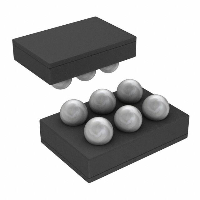
The LM3691 is available in a 6-pin DSBGA package.
Only three external surface-mount components, a
1-μH inductor, a 4.7-μF input capacitor, and a 4.7-μF
output capacitor, are required.
2 Applications
•
•
•
•
The LM3691 has a mode-control pin that allows the
user to select Forced PWM mode or ECO mode that
changes modes between gated PWM mode and
PWM automatically, depending on the load. In ECO
mode, the device offers superior efficiency and very
low IQ under light load conditions. ECO mode extends
the battery life through reduction of the quiescent
current during light load conditions and system
standby.
Mobile Phones
Hand-Held Radios
MP3 Players
Portable Hard Disk Drives
Device Information(1)
PART NUMBER
LM3691
PACKAGE
BODY SIZE (MAX)
DSBGA (6)
1.59 mm × 1.295 mm
(1) For all available packages, see the orderable addendum at
the end of the data sheet.
Typical Application Circuit
IN
A2
B2
CIN
EN
A1
GND C2
LM3691
Efficiency vs. Output Current
(VOUT = 1.8 V, ECO Mode)
VOUT
SW
100
COUT
80
C1 FB
B1 MODE
EFFICIENCY (%)
VIN
2.3 V to 5.5 V
60
VIN = 2.3V
VIN = 3.6V
40
VIN = 4.2V
20
0
0.1
1
10
100
1000
OUTPUT CURRENT (mA)
1
An IMPORTANT NOTICE at the end of this data sheet addresses availability, warranty, changes, use in safety-critical applications,
intellectual property matters and other important disclaimers. PRODUCTION DATA.
�LM3691
SNVS506J – MAY 2008 – REVISED DECEMBER 2015
www.ti.com
Table of Contents
1
2
3
4
5
6
7
8
Features ..................................................................
Applications ...........................................................
Description .............................................................
Revision History.....................................................
Voltage Options .....................................................
Pin Configuration and Functions .........................
Specifications.........................................................
1
1
1
2
3
4
5
7.1
7.2
7.3
7.4
7.5
7.6
5
5
5
5
6
7
Absolute Maximum Ratings ......................................
ESD Ratings..............................................................
Recommended Operating Conditions.......................
Thermal Information ..................................................
Electrical Characteristics ..........................................
Typical Characteristics ..............................................
Detailed Description ............................................ 14
8.1 Overview ................................................................. 14
8.2 Functional Block Diagram ....................................... 14
8.3 Feature Description................................................. 15
8.4 Device Functional Modes........................................ 16
9
Application and Implementation ........................ 17
9.1 Application Information............................................ 17
9.2 Typical Application ................................................. 17
10 Power Supply Recommendations ..................... 20
11 Layout................................................................... 21
11.1 Layout Guidelines ................................................. 21
11.2 Layout Example .................................................... 22
11.3 DSBGA Package Assembly and Use ................... 22
12 Device and Documentation Support ................. 23
12.1
12.2
12.3
12.4
12.5
12.6
Device Support......................................................
Documentation Support ........................................
Community Resources..........................................
Trademarks ...........................................................
Electrostatic Discharge Caution ............................
Glossary ................................................................
23
23
23
23
23
23
13 Mechanical, Packaging, and Orderable
Information ........................................................... 23
4 Revision History
NOTE: Page numbers for previous revisions may differ from page numbers in the current version.
Changes from Revision I (May 2013) to Revision J
•
Added Device Information and Pin Configuration and Functions sections, ESD Ratings table, Feature Description,
Device Functional Modes, Application and Implementation, Power Supply Recommendations, Layout, Device and
Documentation Support, and Mechanical, Packaging, and Orderable Information sections ................................................. 1
Changes from Revision H (April 2013) to Revision I
•
2
Page
Page
Changed layout of National Data Sheet to TI format ........................................................................................................... 22
Submit Documentation Feedback
Copyright © 2008–2015, Texas Instruments Incorporated
Product Folder Links: LM3691
�LM3691
www.ti.com
SNVS506J – MAY 2008 – REVISED DECEMBER 2015
5 Voltage Options
ORDERABLE DEVICE (1) (2)
VOLTAGE OPTION (V)
LM3691TL-0.75/NOPB
0.75
LM3691TLX-0.75/NOPB
0.75
LM3691TL-1.0/NOPB
1
LM3691TLX-1.0/NOPB
1
LM3691TL-1.2/NOPB
1.2
LM3691TLX-1.2/NOPB
1.2
LM3691TL-1.5/NOPB
1.5
LM3691TLX-1.5/NOPB
1.5
LM3691TL-1.8/NOPB
1.8
LM3691TLX-1.8/NOPB
1.8
LM3691TL-2.5/NOPB
2.5
LM3691TLX-2.5/NOPB
2.5
LM3691TL-3.3/NOPB
3.3
LM3691TLX-3.3/NOPB
3.3
(1)
(2)
For the most current package and ordering information, see the Package Option Addendum at the end
of this document, or see the TI web site at www.ti.com.
Package drawings, thermal data, and symbolization are available at www.ti.com/packaging.
Submit Documentation Feedback
Copyright © 2008–2015, Texas Instruments Incorporated
Product Folder Links: LM3691
3
�LM3691
SNVS506J – MAY 2008 – REVISED DECEMBER 2015
www.ti.com
6 Pin Configuration and Functions
YZR Package
6-Pin DSBGA
Top View
YZR Package
6-Pin DSBGA
Bottom View
A1
EN
VIN
A2
A2
VIN
EN
A1
B1
MODE
SW
B2
B2
SW
MODE
B1
C1
FB
GND
C2
C2
GND
FB
C1
Pin Functions
PIN
TYPE (1)
DESCRIPTION
NO.
NAME
A1
EN
I
EN pin. The device is in shutdown mode when voltage to this pin is < 0.4 V and enabled when
> 1.2 V. Do not leave this pin floating
A2
VIN
P
Power supply input. Connect to the input filter capacitor. (See Typical Application Circuit.)
B1
MODE
I
MODE pin: Mode = 1, forced PWM; mode = 0, ECO
Do not leave this pin floating.
B2
SW
A
Switching node connection to the internal PFET switch and NFET synchronous rectifier.
C1
FB
A
Feedback analog input. Connect directly to the output filter capacitor.
(See Typical Application Circuit.)
C2
GND
G
Ground pin.
(1)
4
A: Analog Pin, D: Digital Pin, G: Ground Pin, P: Power Pin, I: Input Pin, I/O; Input/Output, O: Output Pin
Submit Documentation Feedback
Copyright © 2008–2015, Texas Instruments Incorporated
Product Folder Links: LM3691
�LM3691
www.ti.com
SNVS506J – MAY 2008 – REVISED DECEMBER 2015
7 Specifications
7.1 Absolute Maximum Ratings
over operating free-air temperature range (unless otherwise noted) (1) (2)
MIN
MAX
UNIT
−0.2
6
V
(GND − 0.2)
VIN + 0.2
V
150
°C
VIN pin to GND
EN, MODE, FB, SW pins
Junction temperature (TJ-MAX)
Continuous power dissipation (3)
Internally Limited
Maximum lead temperature (soldering, 10 seconds)
260
°C
Storage temperature, Tstg
150
°C
(1)
(2)
(3)
Stresses beyond those listed under Absolute Maximum Ratings may cause permanent damage to the device. These are stress ratings
only, which do not imply functional operation of the device at these or any other conditions beyond those indicated under Recommended
Operating Conditions. Exposure to absolute-maximum-rated conditions for extended periods may affect device reliability.
If Military/Aerospace specified devices are required, contact the TI Sales Office/Distributors for availability and specifications.
Internal thermal shutdown circuitry protects the device from permanent damage. Thermal shutdown engages at TJ = 150°C (typical) and
disengages at TJ = 130°C (typical).
7.2 ESD Ratings
VALUE
V(ESD)
(1)
Electrostatic discharge
Human-body model (HBM), per ANSI/ESDA/JEDEC JS-001
(1)
UNIT
±2000
Machine model
V
±200
JEDEC document JEP155 states that 500-V HBM allows safe manufacturing with a standard ESD control process.
7.3 Recommended Operating Conditions
over operating free-air temperature range (unless otherwise noted)
MIN
Input voltage
NOM
MAX
UNIT
2.3
5.5
0
1000
mA
Junction temperature, TJ
−30
125
°C
Ambient temperature, TA (1)
−30
85
°C
Recommended load current
(1)
V
In applications where high power dissipation and/or poor package resistance is present, the maximum ambient temperature may have to
be derated. Maximum ambient temperature (TA-MAX) is dependent on the maximum operating junction temperature (TJ-MAX), the
maximum power dissipation of the device in the application (PD-MAX) and the junction to ambient thermal resistance of the package
(RθJA) in the application, as given by the following equation: TA-MAX = TJ-MAX − (RθJA × PD-MAX). Due to the pulsed nature of testing the
part, the temp in Electrical Characteristics is specified as TA = TJ.
7.4 Thermal Information
LM3691
THERMAL METRIC
(1)
YZR (DSBGA)
UNIT
6 PINS
RθJA
(1)
(2)
Junction-to-ambient thermal resistance (2)
85
°C/W
For more information about traditional and new thermal metrics, see the Semiconductor and IC Package Thermal Metrics application
report, SPRA953.
Junction-to-ambient thermal resistance is highly application and board layout dependent. In applications where high power dissipation
exists, special care must be given to thermal dissipation issues in board design.
Submit Documentation Feedback
Copyright © 2008–2015, Texas Instruments Incorporated
Product Folder Links: LM3691
5
�LM3691
SNVS506J – MAY 2008 – REVISED DECEMBER 2015
www.ti.com
7.5 Electrical Characteristics
Unless otherwise specified, specifications apply to the LM3691 open-loop Typical Application Circuit with VIN = EN = 3.6 V;
typical limits are for TA = 25°C and minimum and maximum limits apply over the operating ambient temperature range (−30°C
≤ TA = TJ ≤ +85°C). (1) (2) (3)
PARAMETER
TEST CONDITIONS
MIN
TYP
MAX
UNIT
PWM mode
no load VOUT = 1.1 V to 3.3 V
–1%
1%
PWM mode
no load VOUT = 0.75 V to 1 V
–10
10
mV
VFB
Feedback voltage
ISHDN
Shutdown supply current
EN = 0 V
0.03
1
µA
IQ_ECO
ECO mode IQ
ECO mode
64
80
µA
IQ_PWM
PWM mode IQ
PWM mode
490
600
µA
RDSON (P)
Pin-pin resistance for PFET
VIN = VGS = 3.6 V, IO = 200 mA
160
250
mΩ
RDSON (N)
Pin-pin resistance for NFET
VIN = VGS = 3.6 V, IO = −200 mA
115
180
mΩ
ILIM
Switch peak current limit
Open loop
1500
1700
mA
VIH
Logic high input
VIL
Logic low input
IEN,MODE
Input current
FSW
Switching frequency
VON
UVLO threshold (4)
TSTARTUP
(1)
(2)
(3)
(4)
(5)
6
Start time
(5)
1250
1.2
V
0.4
V
0.01
1
4
4.4
MHz
VIN rising, TA = 25°C
2.2
2.29
V
VIN falling
2.1
PWM mode
TA = 25°C
3.6
70
145
µA
V
300
µs
All voltages are with respect to the potential at the GND pin.
Minimum and maximum limits are specified by design, test or statistical analysis. Typical numbers represent the most likely norm.
The parameters in the electrical characteristic table are tested under open-loop conditions at VIN = 3.6 V unless otherwise specified. For
performance over the input voltage range and closed loop condition, refer to the datasheet curves.
The UVLO rising threshold minus the falling threshold is always positive.
Specified by design. Not production tested.
Submit Documentation Feedback
Copyright © 2008–2015, Texas Instruments Incorporated
Product Folder Links: LM3691
�LM3691
www.ti.com
SNVS506J – MAY 2008 – REVISED DECEMBER 2015
7.6 Typical Characteristics
LM3691TL Typical Application Circuit, VIN = 3.6 V, VOUT = 1.8 V, TA = 25°C, L = 1 μH, 2520, (LQM2HP1R0), CIN = COUT = 4.7
μF, 0603(1608), 6.3 V, (C1608X5R0J475K) unless otherwise noted.
Figure 1. Quiescent Supply Current vs Supply Voltage No
Switching, ECO Mode
VOUT = 1.8 V
Figure 2. Quiescent Supply Current vs Supply Voltage No
Switching, PWM Mode
VOUT = 1.8 V
Figure 3. Shutdown Current vs Temperature
VOUT = 0.75 V
Figure 4. Switching Frequency vs Temperature, PWM Mode
VOUT = 1.8 V
Figure 5. Output Voltage vs Supply Voltage
Figure 6. Output Voltage vs Supply Voltage
Submit Documentation Feedback
Copyright © 2008–2015, Texas Instruments Incorporated
Product Folder Links: LM3691
7
�LM3691
SNVS506J – MAY 2008 – REVISED DECEMBER 2015
www.ti.com
Typical Characteristics (continued)
LM3691TL Typical Application Circuit, VIN = 3.6 V, VOUT = 1.8 V, TA = 25°C, L = 1 μH, 2520, (LQM2HP1R0), CIN = COUT = 4.7
μF, 0603(1608), 6.3 V, (C1608X5R0J475K) unless otherwise noted.
VOUT = 0.75 V
VOUT = 1.8 V
Figure 7. Output Voltage vs Output Current
VOUT = 0.75 V
Figure 8. Output Voltage vs Output Current
VOUT = 1.8 V
Figure 9. Input Current vs Output Current
Figure 10. Input Current vs Output Current
100
EFFICIENCY (%)
80
VIN = 2.3V
60
VIN = 3.6V
40
VIN = 4.2V
20
0
0.1
1
10
100
1000
OUTPUT CURRENT (mA)
VOUT = 1.8 V
VOUT = 0.75 V
Figure 11. Efficiency vs, Output Current, ECO Mode
8
Figure 12. Efficiency vs Output Current, ECO Mode
Submit Documentation Feedback
Copyright © 2008–2015, Texas Instruments Incorporated
Product Folder Links: LM3691
�LM3691
www.ti.com
SNVS506J – MAY 2008 – REVISED DECEMBER 2015
Typical Characteristics (continued)
LM3691TL Typical Application Circuit, VIN = 3.6 V, VOUT = 1.8 V, TA = 25°C, L = 1 μH, 2520, (LQM2HP1R0), CIN = COUT = 4.7
μF, 0603(1608), 6.3 V, (C1608X5R0J475K) unless otherwise noted.
100
EFFICIENCY (%)
80
VIN = 4.2V
60
VIN = 3.6V
40
20
0
0.1
1
10
100
1000
OUTPUT CURRENT (mA)
VOUT = 0.75 V
VOUT = 2.5 V
Figure 13. Efficiency vs Output Current, ECO Mode
Figure 14. Efficiency vs Output Current, FPWM Mode
100
VIN = 3.6V
90
EFFICIENCY (%)
VIN = 4.2V
80
70
60
50
40
0
200
400
600
800
1000
OUTPUT CURRENT (mA)
VOUT = 1.8 V
VOUT = 2.5 V
Figure 15. Efficiency vs Output Current, FPWM Mode
Figure 16. Efficiency vs Output Current, FPWM Mode
VOUT = 0.75 V
VOUT = 1.8 V
Figure 17. Load Current Threshold vs Supply Voltage, ECO
Mode to PWM Mode
Figure 18. Load Current Threshold vs Supply Voltage, ECO
Mode to PWM Mode
Submit Documentation Feedback
Copyright © 2008–2015, Texas Instruments Incorporated
Product Folder Links: LM3691
9
�LM3691
SNVS506J – MAY 2008 – REVISED DECEMBER 2015
www.ti.com
Typical Characteristics (continued)
LM3691TL Typical Application Circuit, VIN = 3.6 V, VOUT = 1.8 V, TA = 25°C, L = 1 μH, 2520, (LQM2HP1R0), CIN = COUT = 4.7
μF, 0603(1608), 6.3 V, (C1608X5R0J475K) unless otherwise noted.
VOUT = 0.75 V
VOUT = 1.8 V
Figure 19. Output Voltage Ripple vs Supply Voltage
VOUT = 0.75 V
VOUT = 1.8 V
Figure 21. Closed Loop Current Limit vs Temperature
VOUT = 0.75 V
Figure 22. Closed Loop Current Limit vs Temperature
VOUT = 1.8 V
Figure 23. Line Transient Reponse, PWM Mode
10
Figure 20. Output Voltage Ripple vs Supply Voltage
Figure 24. Line Transient Reponse, PWM Mode
Submit Documentation Feedback
Copyright © 2008–2015, Texas Instruments Incorporated
Product Folder Links: LM3691
�LM3691
www.ti.com
SNVS506J – MAY 2008 – REVISED DECEMBER 2015
Typical Characteristics (continued)
LM3691TL Typical Application Circuit, VIN = 3.6 V, VOUT = 1.8 V, TA = 25°C, L = 1 μH, 2520, (LQM2HP1R0), CIN = COUT = 4.7
μF, 0603(1608), 6.3 V, (C1608X5R0J475K) unless otherwise noted.
VOUT = 0.75 V
ECO Mode 1 mA to 25 mA
VOUT = 0.75 V
Figure 25. Load Transient Reponse
VOUT = 1.8 V
ECO Mode 1 mA to 25 mA
Figure 26. Load Transient Reponse
VOUT = 1.8 V
Figure 27. Load Transient Reponse
VOUT = 0.75 V
ECO Mode to PWM Mode
ECO Mode 25 mA to 1 mA
ECO Mode 25 mA to 1 mA
Figure 28. Load Transient Reponse
VOUT = 0.75 V
Figure 29. Load Transient Reponse
PWM Mode to ECO Mode
Figure 30. Load Transient Reponse
Submit Documentation Feedback
Copyright © 2008–2015, Texas Instruments Incorporated
Product Folder Links: LM3691
11
�LM3691
SNVS506J – MAY 2008 – REVISED DECEMBER 2015
www.ti.com
Typical Characteristics (continued)
LM3691TL Typical Application Circuit, VIN = 3.6 V, VOUT = 1.8 V, TA = 25°C, L = 1 μH, 2520, (LQM2HP1R0), CIN = COUT = 4.7
μF, 0603(1608), 6.3 V, (C1608X5R0J475K) unless otherwise noted.
VOUT = 2.5 V
VOUT = 1.8 V
Figure 32. Load Transient Response
Figure 31. Load Transient Reponse
VOUT = 2.5 V
ECO Mode to PWM Mode
VOUT = 1.8 V
Figure 33. Load Transient Reponse
PWM Mode
PWM Mode
Figure 35. Load Transient Reponse
12
FPWM Mode
Figure 34. Load Transient Reponse
VOUT = 1.8 V
VOUT = 0.75 V
ECO Mode to PWM Mode
ECO Mode to PWM Mode
Submit Documentation Feedback
Figure 36. Load Transient Reponse
Copyright © 2008–2015, Texas Instruments Incorporated
Product Folder Links: LM3691
�LM3691
www.ti.com
SNVS506J – MAY 2008 – REVISED DECEMBER 2015
Typical Characteristics (continued)
LM3691TL Typical Application Circuit, VIN = 3.6 V, VOUT = 1.8 V, TA = 25°C, L = 1 μH, 2520, (LQM2HP1R0), CIN = COUT = 4.7
μF, 0603(1608), 6.3 V, (C1608X5R0J475K) unless otherwise noted.
VOUT = 2.5 V
PWM Mode
VOUT = 0.75 V
Figure 38. Start-Up Into ECO Mode
Figure 37. Load Transient Reponse
VOUT = 0.75 V
ROUT = 2.5 Ω
VOUT = 1.8 V
Figure 39. Start-Up Into PWM Mode
VOUT = 1.8 V
ROUT = 750 Ω
ROUT = 1.8 kΩ
Figure 40. Start-Up Into ECO Mode
ROUT = 6 Ω
Figure 41. Start-Up Into PWM Mode
Submit Documentation Feedback
Copyright © 2008–2015, Texas Instruments Incorporated
Product Folder Links: LM3691
13
�LM3691
SNVS506J – MAY 2008 – REVISED DECEMBER 2015
www.ti.com
8 Detailed Description
8.1 Overview
The LM3691, a high-efficiency, step-down DC-DC switching buck converter, delivers a constant voltage from
either a single Li-Ion or three cell NiMH/NiCd battery to portable devices such as cell phones and PDAs. Using a
voltage mode architecture with synchronous rectification, the LM3691 can deliver up to 1000 mA depending on
the input voltage and output voltage, ambient temperature, and the inductor chosen.
There are three modes of operation depending on the current required: pulse width modulation (PWM), ECO,
and shutdown. The device operates in PWM mode at load currents of approximately 50 mA (typical) or higher.
Lighter output current loads cause the device to automatically switch into ECO mode for reduced current
consumption and a longer battery life. Shutdown mode turns off the device, offering the lowest current
consumption (ISHUTDOWN = 0.03 µA typical). Additional features include soft start, undervoltage protection, current
overload protection, and thermal shutdown protection. As shown in Typical Application Circuit, only three external
power components are required for implementation.
8.2 Functional Block Diagram
14
Submit Documentation Feedback
Copyright © 2008–2015, Texas Instruments Incorporated
Product Folder Links: LM3691
�LM3691
www.ti.com
SNVS506J – MAY 2008 – REVISED DECEMBER 2015
8.3 Feature Description
8.3.1 Circuit Operation
The LM3691 operates as follows. During the first portion of each switching cycle, the control block in the LM3691
turns on the internal PFET switch. This allows current to flow from the input through the inductor to the output
filter capacitor and load. The inductor limits the current to a ramp with a slope of (VIN – VOUT)/L, by storing energy
in a magnetic field. During the second portion of each cycle, the controller turns the PFET switch off, blocking
current flow from the input, and then turns the NFET synchronous rectifier on. The inductor draws current from
ground through the NFET to the output filter capacitor and load, which ramps the inductor current down with a
slope of –VOUT/L.
The output filter stores charge when the inductor current is high, and releases it when low, smoothing the voltage
across the load. The output voltage is regulated by modulating the PFET switch on time to control the average
current sent to the load. The effect is identical to sending a duty-cycle modulated rectangular wave formed by the
switch and synchronous rectifier at the SW pin to a low-pass filter formed by the inductor and output filter
capacitor. The output voltage is equal to the average voltage at the SW pin.
8.3.2 PWM Operation
During PWM operation, the converter operates as a voltage-mode controller with input-voltage feed forward. This
allows the converter to achieve excellent load and line regulation. The DC gain of the power stage is proportional
to the input voltage. To eliminate this dependence, feed forward inversely proportional to the input voltage is
introduced. While in PWM mode, the output voltage is regulated by switching at a constant frequency and then
modulating the energy per cycle to control power to the load. At the beginning of each clock cycle the PFET
switch is turned on, and the inductor current ramps up until the comparator trips and the control logic turns off the
switch. The current limit comparator can also turn off the switch in case the current limit of the PFET is
exceeded. Then the NFET switch is turned on, and the inductor current ramps down. The next cycle is initiated
by the clock turning off the NFET and turning on the PFET.
Figure 42. Typical PWM Operation
8.3.2.1 Internal Synchronous Rectification
While in PWM mode, the LM3691 uses an internal NFET as a synchronous rectifier to reduce rectifier forward
voltage drop and associated power loss. Synchronous rectification provides a significant improvement in
efficiency whenever the output voltage is relatively low compared to the voltage drop across an ordinary rectifier
diode.
8.3.2.2 Current Limiting
A current limit feature allows the LM3691 to protect itself and external components during overload conditions.
PWM mode implements current limit using an internal comparator that trips at 1500 mA (typical). If the output is
shorted to ground, and the output voltage becomes lower than 0.3V (typical), the device enters a timed currentlimit mode where the switching frequency is one fourth, and NFET synchronous rectifier is disabled, thus
preventing excess current and thermal runaway.
Submit Documentation Feedback
Copyright © 2008–2015, Texas Instruments Incorporated
Product Folder Links: LM3691
15
�LM3691
SNVS506J – MAY 2008 – REVISED DECEMBER 2015
www.ti.com
Feature Description (continued)
8.3.3 ECO Operation
Setting the MODE pin low places the LM3691 in Auto mode. By doing so the part switches from ECOnomy
(ECO) state to forced pulse width modulation (FPWM) state based on output load current. At light loads (less
than 50 mA), the converter enters ECO mode. In this mode the part operates with low IQ. During ECO operation,
the converter positions the output voltage slightly higher (30 mV typical) than the nominal output voltage in
FPWM operation. Because the reference is set higher, the output voltage increases to reach the target voltage
when the part goes from sleep state to switching state. Once this voltage is reached the converter enters sleep
mode, thus reducing switching losses and improving light load efficiency. The output voltage ripple is slightly
higher in ECO mode (30 mV peak-to-peak ripple typical).
Figure 43. Typical ECO Operation
8.3.4 Soft-Start
The LM3691 has a soft-start circuit that limits in-rush current during start-up. Output voltage increase rate is
30 mV/µs (at VOUT = 1.8 V typical) during soft start.
8.3.5 Thermal Shutdown Protection
The LM3691 has a thermal overload protection function that operates to protect itself from short-term misuse and
overload conditions. When the junction temperature exceeds around 150°C, the device inhibits operation. Both
the PFET and the NFET are turned off. When the temperature drops below 130°C, normal operation resumes.
Prolonged operation in thermal overload conditions may damage the device and is considered bad practice.
8.3.6 Overtemperature Maximum Load
Table 1. Maximum Overtemperature Load Recommendations
VIN
MAXIMUM LOAD
2.5 V to 5.5 V
1000 mA
2.3 V to 2.5 V
650 mA
8.4 Device Functional Modes
8.4.1 Forced PWM Mode
Setting the MODE pin high (> 1.2 V) places the LM3691 in FPWM. The device is in FPWM regardless of the
load.
8.4.2 Shutdown Mode
Setting the EN input pin low (< 0.4 V) places the LM3691 in shutdown mode. During shutdown the PFET switch,
NFET switch, reference, control and bias circuitry of the LM3691 are turned off. Setting EN high (> 1.2 V)
enables normal operation. When turning on the device with EN soft start is activated. EN pin must be set low to
turn off the LM3691 during system power up and undervoltage conditions when the supply is less than 2.3 V. Do
not leave the EN pin floating.
16
Submit Documentation Feedback
Copyright © 2008–2015, Texas Instruments Incorporated
Product Folder Links: LM3691
�LM3691
www.ti.com
SNVS506J – MAY 2008 – REVISED DECEMBER 2015
9 Application and Implementation
NOTE
Information in the following applications sections is not part of the TI component
specification, and TI does not warrant its accuracy or completeness. TI’s customers are
responsible for determining suitability of components for their purposes. Customers should
validate and test their design implementation to confirm system functionality.
9.1 Application Information
The LM3691 step-down DC-DC converter is optimized for powering ultralow-voltage circuits from a single Li-Ion
cell (2.7 V to 5.5 V) or 3-cell NiMH/NiCd (2.4 V to 4.5 V) batteries. It provides up to 1-A load current over an input
voltage range from 2.3 V to 5.5 V. Seven different fixed voltage output options are available to cover all
commonly used voltage rails (0.75 V, 1 V, 1.2 V, 1.5 V, 1.8 V, 2.5 V, 3.3 V).
9.2 Typical Application
VIN
2.3 V to 5.5 V
L = 1 µH
IN
A2
B2
CIN
4.7 µF
EN
A1
GND C2
LM3691
VOUT
SW
COUT
4.7 µF
C1 FB
B1 MODE
Figure 44. LM3691 Typical Application
9.2.1 Design Requirements
For typical step-down DC-DC applications, use the parameters listed in Table 2.
Table 2. Design Parameters
DESIGN PARAMETER
EXAMPLE VALUE
Minimum input voltage
2.5 V
Minimum output voltage
1.8 V
Output current
150 mA
9.2.2 Detailed Design Procedure
9.2.2.1 Inductor Selection
DC bias current characteristics of inductors must be considered. Different manufacturers follow different
saturation current rating specifications, so attention must be given to details. DC bias curves should be requested
from the manufacturer as part of the inductor selection process.
Minimum value of inductance to specify good performance is 0.5 µH at 1.5 A (ILIM typical) bias current over the
ambient temp range. DC resistance of the inductor must be less than 0.1 Ω for good efficiency at high-current
condition. The inductor AC loss (resistance) also affects conversion efficiency. Higher Q factor at switching
frequency usually gives better efficiency at light load to middle load.
Table 3 lists suggested inductors and suppliers.
Submit Documentation Feedback
Copyright © 2008–2015, Texas Instruments Incorporated
Product Folder Links: LM3691
17
�LM3691
SNVS506J – MAY 2008 – REVISED DECEMBER 2015
www.ti.com
Table 3. Suggested Inductors and Their Suppliers
MODEL
VENDOR
DIMENSIONS L x W x H (mm)
DCR (mΩ)
LQM2HPN1R0MG0
Murata
2.5 × 2.0 × 1.0
55
MLP2520S1R0L
TDK
2.5 × 2.0 × 1.0
60
KSLI252010BG1R0
HItachi Metals
2.5 × 2.0 × 1.0
80
MIPSZ2012D1R0
FDK
2.0 × 1.25 × 1.0
90
9.2.2.2 Input Capacitor Selection
A ceramic input capacitor of 4.7 µF, 6.3 V/10 V is sufficient for most applications. Place the input capacitor as
close as possible to the VIN pin and GND pin of the device. A larger value or higher voltage rating may be used
to improve input voltage filtering. Use X7R, X5R or B types; do not use Y5V or F. DC bias characteristics of
ceramic capacitors must be considered when selecting case sizes like 0402. Minimum input capacitance to
ensure good performance is 2.2 µF at maximum input voltage DC bias including tolerances and over ambient
temperature range.
The input filter capacitor supplies current to the PFET (high-side) switch in the first half of each cycle and
reduces voltage ripple imposed on the input power source. A ceramic capacitor's low ESR provides the best
noise filtering of the input voltage spikes due to this rapidly changing current. Select an input filter capacitor with
sufficient ripple current rating. The input current ripple can be calculated as:
IRMS = IOUTMAX x
r=
VOUT
x
VIN
§1¨
©
2
VOUT
VIN
+
r
12
·
¸
¹
(VIN - VOUT) x VOUT
L x f x IOUTMAX x VIN
(1)
9.2.2.3 Output Capacitor Selection
Use a 4.7-μF, 6.3-V ceramic capacitor, X7R, X5R or B types; do not use Y5V or F. DC bias voltage
characteristics of ceramic capacitors must be considered. DC bias characteristics vary from manufacturer to
manufacturer, and DC bias curves should be requested from the manufacturer as part of the capacitor selection
process. The output filter capacitor smooths out current flow from the inductor to the load, helps maintain a
steady output voltage during transient load changes, and reduces output voltage ripple. These capacitors must
be selected with sufficient capacitance and sufficiently low equivalent series resistance (ESR) to perform these
functions. Minimum output capacitance to specify good performance is 2.2 µF at the output voltage DC bias
including tolerances and over ambient temperature range.
The output voltage ripple is caused by the charging and discharging of the output capacitor and also due to its
RESR and can be calculated as:
Voltage peak-to-peak ripple due to capacitance is shown in Equation 2:
VPP-C =
IRIPPLE
4*f*C
(2)
Voltage peak-to-peak ripple due to ESR Equation 3:
VPP-ESR = (2 × IRIPPLE) × RESR
(3)
Because these two components are out of phase the RMS value can be used to get an approximate value of
peak-to-peak ripple.
Voltage peak-to-peak ripple, root mean squared equals:
VPP-RMS =
VPP-C2 + VPP-ESR2
(4)
Note that the output voltage ripple is dependent on the current ripple and the ESR of the output capacitor (RESR).
The RESR is frequency dependent (as well as temperature dependent); make sure the value used for calculations
is at the switching frequency of the part.
18
Submit Documentation Feedback
Copyright © 2008–2015, Texas Instruments Incorporated
Product Folder Links: LM3691
�LM3691
www.ti.com
SNVS506J – MAY 2008 – REVISED DECEMBER 2015
Table 4 lists suggested capacitors and suppliers.
Table 4. Suggested Capacitors and Their Suppliers
TYPE
VENDOR
VOLTAGE RATING (V)
CASE SIZE
INCH (mm)
C1608X5R0J475K
Ceramic
TDK
6.3
0603 (1608)
C1608X5R1A475K
Ceramic
TDK
10.0
0603 (1608)
MODEL
4.7 µF for CIN and COUT
9.2.3 Application Curves
VOUT = 1.8 V
VOUT = 1.8 V
Figure 46. Load Transient Reponse
Figure 45. Line Transient Reponse, PWM Mode
VOUT = 1.8 V
ECO Mode 25 mA to 1 mA
ECO Mode 1 mA to 25 mA
VOUT = 1.8 V
Figure 47. Load Transient Reponse
ECO Mode to PWM Mode
Figure 48. Load Transient Reponse
Submit Documentation Feedback
Copyright © 2008–2015, Texas Instruments Incorporated
Product Folder Links: LM3691
19
�LM3691
SNVS506J – MAY 2008 – REVISED DECEMBER 2015
VOUT = 1.8 V
www.ti.com
FPWM Mode
VOUT = 1.8 V
Figure 49. Load Transient Reponse
VOUT = 1.8 V
Figure 50. Load Transient Reponse
VOUT = 1.8 V
ROUT = 1.8 kΩ
Figure 51. Start-Up Into ECO Mode
FPWM Mode
ROUT = 6 Ω
Figure 52. Start-Up Into PWM Mode
10 Power Supply Recommendations
The LM3671 is designed to operate from a stable input supply range of 2.3 V to 5.5 V.
20
Submit Documentation Feedback
Copyright © 2008–2015, Texas Instruments Incorporated
Product Folder Links: LM3691
�LM3691
www.ti.com
SNVS506J – MAY 2008 – REVISED DECEMBER 2015
11 Layout
11.1 Layout Guidelines
PC board layout is an important part of DC-DC converter design. Poor board layout can disrupt the performance
of a DC-DC converter and surrounding circuitry by contributing to EMI, ground bounce, and resistive voltage loss
in the traces. These can send erroneous signals to the DC-DC converter device, resulting in poor regulation or
instability. In particular parasitic inductance from extra-long PCB trace lengths can cause additional noise
voltages through L × di/dt that adversely affect the DC-DC converter device circuitry. Good layout for the LM3691
can be implemented by following a few simple design rules.
1. Place the inductor and filter capacitors close together and make the traces short. The traces between these
components carry relatively high switching currents and act as antennas. Following this rule reduces radiated
noise.
2. Place the capacitors and inductor close to the LM3691. Place the CIN capacitor as close to the VIN and GND
pads as possible. Place the COUT capacitor as close to the VOUT and GND connections as possible.
3. Arrange the components so that the switching current loops curl in the same direction. During the first half of
each cycle, current flows from the input filter capacitor, through the buck and inductor to the output filter
capacitor and back through ground, forming a current loop. In the second half of each cycle, current is pulled
up from ground, through the buck by the inductor, to the output filter capacitor and then back through ground,
forming a second current loop. Routing these loops so the current curls in the same direction prevents
magnetic field reversal between the two half-cycles and reduces radiated noise.
4. Connect the ground pins of the buck and filter capacitors together using generous component-side copper fill
as a pseudo-ground plane. Connect this to the ground-plane (if one is used) with several vias. This reduces
ground-plane noise by preventing the switching currents from circulating through the ground plane. It also
reduces ground bounce at the buck by giving it a low-impedance ground connection.
5. Use wide traces between the power components and for power connections to the DC-DC converter circuit.
This reduces voltage errors by resistive losses across the traces. Even 1 mm of fine trace creates parasitic
inductance that can undesirably affect performance from increased L × di/dt noise voltages.
6. Route noise sensitive traces, such as the voltage feedback path, away from noisy traces between the power
components. The voltage feedback trace must remain close to the buck circuit, must be routed directly from
FB to VOUT at the output capacitor, and must be routed opposite to noise components. This reduces EMI
radiated onto the voltage feedback trace of the DC-DC converter.
Submit Documentation Feedback
Copyright © 2008–2015, Texas Instruments Incorporated
Product Folder Links: LM3691
21
�LM3691
SNVS506J – MAY 2008 – REVISED DECEMBER 2015
www.ti.com
11.2 Layout Example
VIN
SW
GND
EN
MODE
FB
KEY
VIA TO GROUND PLANE
VIA TO SIGNAL/POWER PLANE
TOP LAYER
BOTTOM LAYER
Figure 53. LM3291 Layout Example
11.3 DSBGA Package Assembly and Use
Use of the DSBGA package requires specialized board layout, precision mounting, and careful re-flow
techniques, as detailed in TI Application Note DSBGA Wafer Level Chip Scale Package (SNVA009). Refer to the
section Surface Mount Assembly Considerations. For best results in assembly, alignment ordinals on the PC
board must be used to facilitate placement of the device. The pad style used with DSBGA package must be the
NSMD (non-solder mask defined) type. This means that the solder-mask opening is larger than the pad size.
This prevents a lip that otherwise forms if the solder-mask and pad overlap, from holding the device off the
surface of the board and interfering with mounting. See SNVA009 for specific instructions how to do this.
The 6-pin package used for LM3691 has 300-micron solder balls and requires 10.82 mils pads for mounting on
the circuit board. The trace to each pad must enter the pad with a 90° entry angle to prevent debris from being
caught in deep corners. Initially, the trace to each pad must be 7-mil wide, for a section approximately 7-mil long
or longer, as a thermal relief. Then each trace must neck up or down to its optimal width. The important criteria is
symmetry. This ensures the solder bumps on the LM3691 re-flow evenly and that the device solders level to the
board. In particular, special attention must be paid to the pads for bumps A2 and C2, because GND and VIN are
typically connected to large copper planes.
The DSBGA package is optimized for the smallest possible size in applications with red or infrared opaque
cases. Because the DSBGA package lacks the plastic encapsulation characteristic of larger devices, it is
vulnerable to light. Backside metallization and/or epoxy coating, along with front side shading by the printed
circuit board, reduce this sensitivity. However, the package has exposed die edges. In particular, DSBGA
devices are sensitive to light, in the red and infrared range, shining on the exposed die edges of the package.
22
Submit Documentation Feedback
Copyright © 2008–2015, Texas Instruments Incorporated
Product Folder Links: LM3691
�LM3691
www.ti.com
SNVS506J – MAY 2008 – REVISED DECEMBER 2015
12 Device and Documentation Support
12.1 Device Support
12.1.1 Third-Party Products Disclaimer
TI'S PUBLICATION OF INFORMATION REGARDING THIRD-PARTY PRODUCTS OR SERVICES DOES NOT
CONSTITUTE AN ENDORSEMENT REGARDING THE SUITABILITY OF SUCH PRODUCTS OR SERVICES
OR A WARRANTY, REPRESENTATION OR ENDORSEMENT OF SUCH PRODUCTS OR SERVICES, EITHER
ALONE OR IN COMBINATION WITH ANY TI PRODUCT OR SERVICE.
12.2 Documentation Support
12.2.1 Related Documentation
For additional information, see the following:
TI Application Note DSBGA Wafer Level Chip Scale Package (SNVA009)
12.3 Community Resources
The following links connect to TI community resources. Linked contents are provided "AS IS" by the respective
contributors. They do not constitute TI specifications and do not necessarily reflect TI's views; see TI's Terms of
Use.
TI E2E™ Online Community TI's Engineer-to-Engineer (E2E) Community. Created to foster collaboration
among engineers. At e2e.ti.com, you can ask questions, share knowledge, explore ideas and help
solve problems with fellow engineers.
Design Support TI's Design Support Quickly find helpful E2E forums along with design support tools and
contact information for technical support.
12.4 Trademarks
E2E is a trademark of Texas Instruments.
All other trademarks are the property of their respective owners.
12.5 Electrostatic Discharge Caution
This integrated circuit can be damaged by ESD. Texas Instruments recommends that all integrated circuits be handled with
appropriate precautions. Failure to observe proper handling and installation procedures can cause damage.
ESD damage can range from subtle performance degradation to complete device failure. Precision integrated circuits may be more
susceptible to damage because very small parametric changes could cause the device not to meet its published specifications.
12.6 Glossary
SLYZ022 — TI Glossary.
This glossary lists and explains terms, acronyms, and definitions.
13 Mechanical, Packaging, and Orderable Information
The following pages include mechanical, packaging, and orderable information. This information is the most
current data available for the designated devices. This data is subject to change without notice and revision of
this document. For browser-based versions of this data sheet, refer to the left-hand navigation.
Submit Documentation Feedback
Copyright © 2008–2015, Texas Instruments Incorporated
Product Folder Links: LM3691
23
�PACKAGE OPTION ADDENDUM
www.ti.com
10-Dec-2020
PACKAGING INFORMATION
Orderable Device
Status
(1)
Package Type Package Pins Package
Drawing
Qty
Eco Plan
(2)
Lead finish/
Ball material
MSL Peak Temp
Op Temp (°C)
Device Marking
(3)
(4/5)
(6)
LM3691TL-0.75/NOPB
ACTIVE
DSBGA
YZR
6
250
RoHS & Green
SNAGCU
Level-1-260C-UNLIM
-30 to 85
V
LM3691TL-1.0/NOPB
ACTIVE
DSBGA
YZR
6
250
RoHS & Green
SNAGCU
Level-1-260C-UNLIM
LM3691TL-1.2/NOPB
ACTIVE
DSBGA
YZR
6
250
RoHS & Green
SNAGCU
Level-1-260C-UNLIM
-30 to 85
X
LM3691TL-1.5/NOPB
ACTIVE
DSBGA
YZR
6
250
RoHS & Green
SNAGCU
Level-1-260C-UNLIM
-30 to 85
Y
LM3691TL-1.8/NOPB
ACTIVE
DSBGA
YZR
6
250
RoHS & Green
SNAGCU
Level-1-260C-UNLIM
-30 to 85
Z
LM3691TL-2.5/NOPB
ACTIVE
DSBGA
YZR
6
250
RoHS & Green
SNAGCU
Level-1-260C-UNLIM
8
LM3691TL-3.3/NOPB
ACTIVE
DSBGA
YZR
6
250
RoHS & Green
SNAGCU
Level-1-260C-UNLIM
T
LM3691TLX-1.0/NOPB
ACTIVE
DSBGA
YZR
6
3000
RoHS & Green
SNAGCU
Level-1-260C-UNLIM
F
LM3691TLX-1.2/NOPB
ACTIVE
DSBGA
YZR
6
3000
RoHS & Green
SNAGCU
Level-1-260C-UNLIM
-30 to 85
X
LM3691TLX-1.5/NOPB
ACTIVE
DSBGA
YZR
6
3000
RoHS & Green
SNAGCU
Level-1-260C-UNLIM
-30 to 85
Y
LM3691TLX-1.8/NOPB
ACTIVE
DSBGA
YZR
6
3000
RoHS & Green
SNAGCU
Level-1-260C-UNLIM
-30 to 85
Z
LM3691TLX-2.5/NOPB
ACTIVE
DSBGA
YZR
6
3000
RoHS & Green
SNAGCU
Level-1-260C-UNLIM
8
LM3691TLX-3.3/NOPB
ACTIVE
DSBGA
YZR
6
3000
RoHS & Green
SNAGCU
Level-1-260C-UNLIM
T
F
(1)
The marketing status values are defined as follows:
ACTIVE: Product device recommended for new designs.
LIFEBUY: TI has announced that the device will be discontinued, and a lifetime-buy period is in effect.
NRND: Not recommended for new designs. Device is in production to support existing customers, but TI does not recommend using this part in a new design.
PREVIEW: Device has been announced but is not in production. Samples may or may not be available.
OBSOLETE: TI has discontinued the production of the device.
(2)
RoHS: TI defines "RoHS" to mean semiconductor products that are compliant with the current EU RoHS requirements for all 10 RoHS substances, including the requirement that RoHS substance
do not exceed 0.1% by weight in homogeneous materials. Where designed to be soldered at high temperatures, "RoHS" products are suitable for use in specified lead-free processes. TI may
reference these types of products as "Pb-Free".
RoHS Exempt: TI defines "RoHS Exempt" to mean products that contain lead but are compliant with EU RoHS pursuant to a specific EU RoHS exemption.
Green: TI defines "Green" to mean the content of Chlorine (Cl) and Bromine (Br) based flame retardants meet JS709B low halogen requirements of


 工商网监
湘ICP备2023018690号
工商网监
湘ICP备2023018690号
