Product
Folder
Sample &
Buy
Support &
Community
Tools &
Software
Technical
Documents
LM3704
SNVS088F – MAY 2004 – REVISED APRIL 2016
LM3704 Voltage Supervisor With Power-Fail Input,
Low-Line Output and Manual Reset
1 Features
3 Description
•
•
•
•
The LM3704 is a feature-rich, easy-to-use voltage
supervisor. It is offered in both push-pull and opendrain configuration with a tight 2% accuracy over
temperature.
1
•
•
•
•
•
Available Threshold Voltage of 3.08 V and 2.32 V
No External Components Required
Manual-Reset Input
Available in Both Open-Drain and Push-Pull
Configuration
Reset Time-Out Delay of 200 ms
Separate Power-Fail Comparator
±0.5% Reset Threshold Accuracy at Room
Temperature
±2% Reset Threshold Accuracy Over
Temperature
28-µA VCC Supply Current
Device Information(1)
PART NUMBER
LM3704
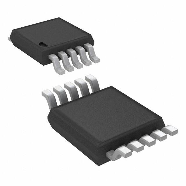
PACKAGE
VSSOP (10)
BODY SIZE (NOM)
3.00 mm × 3.00 mm
(1) For all available packages, see the orderable addendum at
the end of the data sheet.
2 Applications
•
•
•
•
The LM3704 features include a manual reset, low-line
output, and power-fail input detection. The power-fail
input allows for a configurable second rail to be
monitored helping detect upstream failures. The lowline output is used as a second interrupt line to
indicate a fall in VCC (1.02 × VRST).
Embedded Controllers and Processors
Intelligent Instruments
Automotive Systems
Critical µP Power Monitoring
Typical Application
VIN1
VCC
VIN2
VCC
Reset
Reset
PFI
PFO
NMI
LLO
INT
PP
MR
GND
GND
Copyright © 2016, Texas Instruments Incorporated
1
An IMPORTANT NOTICE at the end of this data sheet addresses availability, warranty, changes, use in safety-critical applications,
intellectual property matters and other important disclaimers. PRODUCTION DATA.
�LM3704
SNVS088F – MAY 2004 – REVISED APRIL 2016
www.ti.com
Table of Contents
1
2
3
4
5
6
7
Features ..................................................................
Applications ...........................................................
Description .............................................................
Revision History.....................................................
Pin Configuration and Functions .........................
Specifications.........................................................
1
1
1
2
3
4
6.1
6.2
6.3
6.4
6.5
6.6
4
4
4
4
5
8
Absolute Maximum Ratings ......................................
ESD Ratings..............................................................
Recommended Operating Conditions.......................
Thermal Information ..................................................
Electrical Characteristics...........................................
Typical Characteristics ..............................................
Detailed Description ............................................ 10
7.1 Overview ................................................................. 10
7.2 Functional Block Diagram ....................................... 10
7.3 Feature Description................................................. 10
7.4 Device Functional Modes........................................ 11
8
Application and Implementation ........................ 12
8.1 Application Information............................................ 12
8.2 Typical Application ................................................. 12
8.3 System Examples ................................................... 14
9 Power Supply Recommendations...................... 16
10 Layout................................................................... 16
10.1 Layout Guidelines ................................................. 16
10.2 Layout Example .................................................... 16
11 Device and Documentation Support ................. 17
11.1
11.2
11.3
11.4
11.5
Device Support......................................................
Community Resources..........................................
Trademarks ...........................................................
Electrostatic Discharge Caution ............................
Glossary ................................................................
17
17
17
17
17
12 Mechanical, Packaging, and Orderable
Information ........................................................... 17
4 Revision History
NOTE: Page numbers for previous revisions may differ from page numbers in the current version.
Changes from Revision E (November 2012) to Revision F
•
2
Page
Added ESD Ratings table, Feature Description section, Device Functional Modes, Application and Implementation
section, Power Supply Recommendations section, Layout section, Device and Documentation Support section, and
Mechanical, Packaging, and Orderable Information section .................................................................................................. 1
Submit Documentation Feedback
Copyright © 2004–2016, Texas Instruments Incorporated
Product Folder Links: LM3704
�LM3704
www.ti.com
SNVS088F – MAY 2004 – REVISED APRIL 2016
5 Pin Configuration and Functions
DGS Package
10-Pin VSSOP
Top View
VCC
1
10
RESET
MR
2
9
NC
PFI
3
8
PFO
NC
4
7
LLO
GND
5
6
NC
Pin Functions
PIN
NO.
NAME
I/O
DESCRIPTION
1
VCC
I
Power supply input.
2
MR
I
Manual-reset input. When MR is less than VMRT (manual reset threshold) RESET/RESET is engaged.
3
PFI
I
Power-fail comparator input. When PFI is less than VPFT (power-fail reset threshold), the PFO goes low.
Otherwise, PFO remains high.
4
NC
—
No connection.
5
GND
—
Ground reference for all signals.
6
NC
—
No connection.
7
LLO
O
Low-line logic output. Early power-fail warning output. Low when VCC falls below VLLOT (low-line output
threshold). This output can be used to generate an NMI (non-maskable interrupt) to provide an early
warning of imminent power failure.
8
PFO
O
Power-fail logic output. When PFI is below VPFT, PFO goes low; otherwise, PFO remains high.
9
NC
—
No connection. Test input used at factory only. Leave floating.
10
RESET
O
Reset logic output. Pulses low for tRP (reset time-out period) when triggered, and stays low whenever
VCC is below the reset threshold or when MR is below VMRT. It remains low for tRP after either VCC rises
above the reset threshold, or after MR input rises above VMRT.
Submit Documentation Feedback
Copyright © 2004–2016, Texas Instruments Incorporated
Product Folder Links: LM3704
3
�LM3704
SNVS088F – MAY 2004 – REVISED APRIL 2016
www.ti.com
6 Specifications
6.1 Absolute Maximum Ratings
over operating free-air temperature range (unless otherwise noted) (1)
MIN
MAX
UNIT
Supply voltage, VCC
–0.3
6
V
All other inputs
–0.3
VCC + 0.3
V
See (2)
Power dissipation
Storage temperature, Tstg
(1)
(2)
–65
150
°C
Stresses beyond those listed under Absolute Maximum Ratings may cause permanent damage to the device. These are stress ratings
only, which do not imply functional operation of the device at these or any other conditions beyond those indicated under Recommended
Operating Conditions. Exposure to absolute-maximum-rated conditions for extended periods may affect device reliability.
The maximum allowable power dissipation is a function of the maximum junction temperature, TJ(MAX), the junction-to-ambient thermal
resistance, θJ-A, and the ambient temperature, TA. The maximum allowable power dissipation at any ambient temperature is calculated
using:
P(MAX) =
TJ (MAX) - TA
qJ - A
Where the value of θJ-A for the 10-pin VSSOP package is 195°C/W in a typical printed-circuit board (PCB) mounting and the DSBGA
package is 220°C/W.
6.2 ESD Ratings
VALUE
V(ESD)
(1)
(2)
Electrostatic discharge
Human-body model (HBM), per ANSI/ESDA/JEDEC JS-001 (1)
±1500
Charged-device model (CDM), per JEDEC specification JESD22-C101 (2)
±150
UNIT
V
JEDEC document JEP155 states that 500-V HBM allows safe manufacturing with a standard ESD control process.
JEDEC document JEP157 states that 250-V CDM allows safe manufacturing with a standard ESD control process.
6.3 Recommended Operating Conditions
over operating free-air temperature range (unless otherwise noted)
TA
Free-air temperature
MIN
MAX
–40
85
UNIT
°C
6.4 Thermal Information
LM3704
THERMAL METRIC (1)
DGS (VSSOP)
UNIT
10 PINS
RθJA
Junction-to-ambient thermal resistance
163.7
°C/W
RθJC(top)
Junction-to-case (top) thermal resistance
58.3
°C/W
RθJB
Junction-to-board thermal resistance
83.5
°C/W
ψJT
Junction-to-top characterization parameter
6
°C/W
ψJB
Junction-to-board characterization parameter
82.2
°C/W
RθJC(bot)
Junction-to-case (bottom) thermal resistance
—
°C/W
(1)
4
For more information about traditional and new thermal metrics, see the Semiconductor and IC Package Thermal Metrics application
report, SPRA953.
Submit Documentation Feedback
Copyright © 2004–2016, Texas Instruments Incorporated
Product Folder Links: LM3704
�LM3704
www.ti.com
SNVS088F – MAY 2004 – REVISED APRIL 2016
6.5 Electrical Characteristics
at TJ = 25°C and VCC = 2.2 V to 5.5 V (unless otherwise noted)
PARAMETER
TEST CONDITIONS
MIN
TYP
MAX UNIT
POWER SUPPLY
VCC
ICC
Operating voltage
VCC supply current
LM3704, TJ = –40°C to 85°C
All inputs = VCC,
all outputs floating
1
TJ = 25°C
5.5
28
TJ = –40°C to 85°C
50
V
µA
RESET THRESHOLD
TJ = 25°C
VRST
Reset threshold
VRSTH
Reset threshold hysteresis
VCC falling
TJ = –40°C to 85°C
TJ = 0°C to 70°C
–0.5%
VRST
–2%
0.5%
2%
–1.5%
1.5%
0.0032 × VRST
tRP
Reset time-out period
Reset time-out period =
C
tRD
VCC to reset delay
VCC falling at 1 mV/µs
TJ = 25°C
TJ = –40°C to 85°C
mV
200
140
280
20
ms
µs
RESET
VOL
VOH
RESET
RESET
VCC > 1.0 V, ISINK = 50 µA,
TJ = –40°C to 85°C
0.3
VCC > 1.2 V, ISINK = 100 µA,
TJ = –40°C to 85°C
0.3
VCC > 2.25 V, ISINK = 900 µA,
TJ = –40°C to 85°C
0.3
VCC > 2.7 V, ISINK = 1.2 mA,
TJ = –40°C to 85°C
0.3
VCC > 4.5 V, ISINK = 3.2 mA,
TJ = –40°C to 85°C
0.4
VCC > 2.25 V, ISOURCE = 300 µA,
TJ = –40°C to 85°C
0.8 × VCC
VCC > 2.7 V, ISOURCE = 500 µA,
TJ = –40°C to 85°C
0.8 × VCC
VCC > 4.5 V, ISOURCE = 800 µA,
TJ = –40°C to 85°C
VCC − 1.5
V
V
PFI/MR
TJ = 25°C
1.225
VPFT
PFI input threshold
VMRT
MR Input threshold
TJ = –40°C to 85°C
VPFTH/
VMRTH
PFI/MR threshold
hysteresis
PFI/MR falling, VCC = VRST MAX to 5.5 V
IPFI
Input current (PFI only)
TJ = –40°C to 85°C
RMR
MR pullup resistance
tMD
MR to reset delay
tMR
MR pulse width
TJ = –40°C to 85°C
1.2
1.25
MR, low
MR, high
0.8
2
0.0032 × VRST
–75
TJ = 25°C
35
TJ = –40°C to 85°C
25
V
mV
75
56
TJ = –40°C to 85°C
V
75
12
nA
kΩ
µS
µS
PFO, LLO
VOL
PFO, LLO output low
voltage
VCC > 2.25 V, ISINK = 900 µA,
TJ = –40°C to 85°C
0.3
VCC > 2.7 V, ISINK = 1.2 mA,
TJ = –40°C to 85°C
0.3
VCC > 4.5 V, ISINK = 3.2 mA,
TJ = –40°C to 85°C
0.4
Submit Documentation Feedback
Copyright © 2004–2016, Texas Instruments Incorporated
Product Folder Links: LM3704
V
5
�LM3704
SNVS088F – MAY 2004 – REVISED APRIL 2016
www.ti.com
Electrical Characteristics (continued)
at TJ = 25°C and VCC = 2.2 V to 5.5 V (unless otherwise noted)
PARAMETER
VOH
PFO, LLO output high
voltage
TEST CONDITIONS
MIN
VCC > 2.25 V, ISOURCE = 300 µA,
TJ = –40°C to 85°C
0.8 VCC
VCC > 2.7 V, ISOURCE = 500 µA,
TJ = –40°C to 85°C
0.8 VCC
VCC > 4.5 V, ISOURCE = 800 µA,
TJ = –40°C to 85°C
VCC − 1.5
TYP
MAX UNIT
V
LLO OUTPUT
VLLOT
LLO output threshold
VLLOTH
Low-line comparator
hysteresis
tCD
Low-line comparator delay
VLLO − VRST, VCC falling
TJ = 25°C
TJ = –40°C to 85°C
1.02 × VRST
1.01 × VRST
VCC falling at 1 mV/µs
1.03 × VRST
V
0.0032 × VRST
mV
20
µs
Figure 1. LM3704 Reset Time With MR
Figure 2. LLO Output
6
Submit Documentation Feedback
Copyright © 2004–2016, Texas Instruments Incorporated
Product Folder Links: LM3704
�LM3704
www.ti.com
SNVS088F – MAY 2004 – REVISED APRIL 2016
Figure 3. PFI Comparator Timing Diagram
Submit Documentation Feedback
Copyright © 2004–2016, Texas Instruments Incorporated
Product Folder Links: LM3704
7
�LM3704
SNVS088F – MAY 2004 – REVISED APRIL 2016
www.ti.com
30
30
25
29
Supply Current (PA)
Supply Current (PA)
6.6 Typical Characteristics
20
15
10
5
0
1
2
3
4
Supply Voltage (V)
26
25
23
-40
5
220
0.4
215
0.3
0.2
0.1
0
-0.1
-0.2
-0.3
-0.4
-0.5
-40
25
Temperature (°C)
25
70
Temperature (°C)
85
210
205
200
195
190
185
180
3.0
85
3.5
4
4.5
5
5.5
6
Supply Voltage (V)
Figure 6. Normalized Reset Threshold Voltage
vs Temperature
Figure 7. Reset Timeout Period vs VCC
215
Maximum Transient Duration (Ps)
80
210
205
200
195
190
-40
0
Figure 5. 3.3-V Supply Current vs Temperature
0.5
Reset Timeout Period (ms)
Normalized Threshold Voltage (%)
27
24
Figure 4. Supply Current vs Supply Voltage
Reset Timeout Period (ms)
28
70
60
50
40
30
20
10
0
25
10
85
100
Temperature (°C)
1000
Reset Comparator Overdrive (mV)
VRST - VCC
VCC = 3.3 V
Figure 8. Reset Timeout Period vs Temperature
8
Submit Documentation Feedback
Figure 9. Maximum Transient Duration
vs Reset Comparator Overdrive
Copyright © 2004–2016, Texas Instruments Incorporated
Product Folder Links: LM3704
�LM3704
www.ti.com
SNVS088F – MAY 2004 – REVISED APRIL 2016
Typical Characteristics (continued)
39
Propagation Delay (Ps)
37
35
33
31
29
27
25
-40
-20
0
20
40
60
80
Temperature (oC)
Figure 10. Low-Line Comparator Propagation Delay vs Temperature
Submit Documentation Feedback
Copyright © 2004–2016, Texas Instruments Incorporated
Product Folder Links: LM3704
9
�LM3704
SNVS088F – MAY 2004 – REVISED APRIL 2016
www.ti.com
7 Detailed Description
7.1 Overview
The LM3704 microprocessor supervisory circuit monitors power supplies and battery-controlled functions in
systems and does not require external components. There is a standard reset threshold voltage of 3.08 V while
other custom reset threshold voltages are available to provide maximum monitoring flexibility. The RESET pin
pulses low for the reset time-out period when triggered and stays low whenever VCC is below the reset threshold
or when MR is below VMRT. Once the VCC rises above the reset threshold, or after MR input rises above VMRT,
the RESET pin remains low for the reset timeout period before coming up.
7.2 Functional Block Diagram
VCC
Reset Detect
+
LLO
Comparator
56 k
Reset Logic &
One-Shot
Timer
OPEN for 'Y' versions;
CONNECT for 'X'
versions
RESET/RESET
OUTPUT
+
LLO
-
Manual Reset
Comparator
+
MR
Power Fail
Comparator
PFI
+
PFO
-
Bandgap Reference
1.225 V
Copyright © 2016, Texas Instruments Incorporated
7.3 Feature Description
7.3.1 Reset Output
The reset input of a µP initializes the device into a known state. The LM3704 microprocessor supervisory circuit
asserts a forced reset output to prevent code execution errors during power-up, power-down, and brownout
conditions.
RESET is ensured valid for VCC > 1 V. Once VCC exceeds the reset threshold, an internal timer maintains the
output for the reset time-out period. After this interval, reset goes high. The LM3704 offers an active-low RESET.
Any time VCC drops below the reset threshold (such as during a brownout), the reset activates. When VCC again
rises above the reset threshold, the internal timer starts. Reset holds until VCC exceeds the reset threshold for
longer than the reset time-out period. After this time, reset releases.
10
Submit Documentation Feedback
Copyright © 2004–2016, Texas Instruments Incorporated
Product Folder Links: LM3704
�LM3704
www.ti.com
SNVS088F – MAY 2004 – REVISED APRIL 2016
Feature Description (continued)
The Manual Reset input (MR) initiates a forced reset also. See Manual Reset Input (MR).
7.3.2 Reset Threshold
The LM3704 is available with a reset voltage of 3.08 V. Other reset thresholds in the 2.20-V to 5-V range, in
steps of 10 mV, are available; contact Texas Instruments for details.
7.3.3 Manual Reset Input (MR)
Many µP-based products require a manual reset capability, allowing the operator to initiate a reset. The MR input
is fully debounced and provides an internal 56-kΩ pullup. When the MR input is pulled below VMRT (1.225 V) for
more than 25 µs, reset is asserted after a typical delay of 12 µs. Reset remains active as long as MR is held low,
and releases after the reset time-out period expires after MR rises above VMRT. Use MR with digital logic to
assert or to daisy chain supervisory circuits. It may be used as another low-line comparator by adding a buffer.
7.3.4 Power-Fail Comparator (PFI/PFO)
The PFI is compared to a 1.225-V internal reference, VPFT. If PFI is less than VPFT, the Power-Fail Output (PFO)
drops low. The power-fail comparator signals a falling power supply, and is driven typically by an external voltage
divider that senses either the unregulated supply or another system supply voltage. The voltage divider generally
is chosen so the voltage at PFI drops below VPFT several milliseconds before the main supply voltage drops
below the reset threshold, providing advanced warning of a brownout.
The voltage threshold is set by R1 and R2 and is calculated with Equation 1.
VPFT =
R1 + R2
x 1.225V
R2
(1)
NOTE
This comparator is completely separate from the rest of the circuitry, and may be
employed for other functions as needed.
7.3.5 Low-Line Output (LLO)
The low-line output comparator is typically used to provide a non-maskable interrupt to a µP when VCC begins
falling. LLO monitors VCC and goes low when VCC falls below VLLOT (typically 1.02 × VRST) with hysteresis of
0.0032 × VRST.
7.4 Device Functional Modes
7.4.1 RESET Output Low
Anytime VCC drops below the reset threshold, the RESET output drops low and remains low until VCC rises above
the threshold and the reset time-out period has expired. The manual reset input (MR) also causes the reset to be
active. If MR input is pulled below VMRT for more than 25 µs, the RESET output drops low and remains low until
MR rises above the manual reset threshold (VMRT) and the reset time-out period has expired.
7.4.2 RESET Output High
The RESET output remains high as long as VCC is above the reset threshold and MR is above the manual reset
threshold (VMRT).
Submit Documentation Feedback
Copyright © 2004–2016, Texas Instruments Incorporated
Product Folder Links: LM3704
11
�LM3704
SNVS088F – MAY 2004 – REVISED APRIL 2016
www.ti.com
8 Application and Implementation
NOTE
Information in the following applications sections is not part of the TI component
specification, and TI does not warrant its accuracy or completeness. TI’s customers are
responsible for determining suitability of components for their purposes. Customers should
validate and test their design implementation to confirm system functionality.
8.1 Application Information
The LM3704 is a microprocessor supervisory circuit that provides the maximum flexibility for monitoring power
supplies and battery-controlled functions. The reset threshold is typically 3.08 V but can be customized for
voltages between 2.2 V and 5 V in 10-mV increments by contacting Texas Instruments. The power-fail input,
which is a 1.225-V threshold detector for power-fail warning, can be adjusted using a resistor divider as shown in
Figure 11. This section shows various application circuits to provide different monitoring solutions.
8.2 Typical Application
VIN2
VIN1
VCC
R1
RESE
T
RESET
PFI
PP
LLO
INT
R2
MR
PFO
GND
GND
(
. R1
Power-Fail Reset Threshold, VPFT = 1.225 (
+1
R2
Copyright © 2016, Texas Instruments Incorporated
Figure 11. Monitoring Two Critical Supplies
8.2.1 Design Requirements
The component count is minimal; employing two resistors as part of a voltage-divider circuit is all that is needed
for the typical application of monitoring two critical supplies shown in Figure 11.
8.2.2 Detailed Design Procedure
The voltage-divider circuit that connects to the power-fail reset pin is chosen such that the reset threshold at the
device is 1.225 V as shown in Figure 11.
12
Submit Documentation Feedback
Copyright © 2004–2016, Texas Instruments Incorporated
Product Folder Links: LM3704
�LM3704
www.ti.com
SNVS088F – MAY 2004 – REVISED APRIL 2016
Typical Application (continued)
8.2.3 Application Curves
VIN1 = VCC
*Reset Threshold
tRP
RESET
Standard reset threshold is 3.08 V. Custom reset voltages are available between 2.2 V and 5 V in 10-mV increments
by contacting Texas Instruments.
Figure 12. Monitoring VIN1 for Reset Condition
VIN2
Threshold set by R1 and R2 voltage-divider
PFI
VPFT =1.225 V
PFO
MR
VMRT =1.225 V
tRP
RESET
See Electrical Characteristics for high and low levels of this specific application.
Figure 13. Monitoring VIN2 for Reset Condition
Submit Documentation Feedback
Copyright © 2004–2016, Texas Instruments Incorporated
Product Folder Links: LM3704
13
�LM3704
SNVS088F – MAY 2004 – REVISED APRIL 2016
www.ti.com
8.3 System Examples
The LM3704 voltage supervisor has various features such as power-fail input detection, low-line output, and
manual reset while requiring few to no additional components making it versatile and easy-to-use. See Figure 14
through Figure 18 for a variety of circuit applications.
spacer
1.8V
1.8V
3.3V
3.3V
107k
107k
VI/O
VCC
PFI
VCC
Vcore
RESET
PFI
RESET
RESET
VI/O
VCORE
RESET
332k
332k
MR
PFO
MR
PFO
GND
GND
3.3k
FAULT
(Normally
High)
Copyright © 2016, Texas Instruments Incorporated
Copyright © 2016, Texas Instruments Incorporated
Figure 14. Monitoring Two Supplies Plus Manual
Reset
Raw Supply
(Battery)
Figure 15. Monitoring Dual Supplies
Plus External Fault Input
System
Regulator
3.3V
0.1P ceramic
R1
R2
VCC
PFI
PFO
MR
RESET
INT
PP
RESET
GND
(
. R1
Power-Fail Reset Threshold, VPFT = 1.225 (
+1
R2
Copyright © 2016, Texas Instruments Incorporated
MR input with its 1.225-V nominal threshold, may monitor an additional supply voltage. An internal 56-kΩ
pullup resistor is included on this input.
Figure 16. Microprocessor Supervisor
With Early Warning Detector
14
Submit Documentation Feedback
Copyright © 2004–2016, Texas Instruments Incorporated
Product Folder Links: LM3704
�LM3704
www.ti.com
SNVS088F – MAY 2004 – REVISED APRIL 2016
System Examples (continued)
IN
VIN
VOUT
OUT
LM2941
SD
GND
24.9k
+
2.2PF
ADJ
7.15k
14.7k
11.5k
VOUT = 3.3V
VCC
VIN(TRIP) = 5.0V
RESET
MR
OVERRIDE
5V
4V
VIN
3.3V
VOUT
RESET
tRP
Copyright © 2016, Texas Instruments Incorporated
Figure 17. Regulator/Switch With Long-Term Overvoltage Lockout
Prevents Overdissipation in Linear Regulator
3.3V
VCC
RESET
MR
RESET
tRP
GND
Mechanical
Switch
tRP
MR
Copyright © 2016, Texas Instruments Incorporated
Figure 18. Switch Debouncer
Submit Documentation Feedback
Copyright © 2004–2016, Texas Instruments Incorporated
Product Folder Links: LM3704
15
�LM3704
SNVS088F – MAY 2004 – REVISED APRIL 2016
www.ti.com
9 Power Supply Recommendations
The input power supply to the VCC pin of the LM3704 must be kept at a voltage lower than the recommended
voltage of 5.5 V. All other input pins must be kept at a voltage lower than VCC + 0.3 V. Do not exceed absolute
maximum ratings found in Absolute Maximum Ratings in any circumstance.
10 Layout
10.1 Layout Guidelines
Keep traces short between IC and external components.
10.2 Layout Example
Figure 19. Layout Example for Application Circuit
16
Submit Documentation Feedback
Copyright © 2004–2016, Texas Instruments Incorporated
Product Folder Links: LM3704
�LM3704
www.ti.com
SNVS088F – MAY 2004 – REVISED APRIL 2016
11 Device and Documentation Support
11.1 Device Support
11.1.1 Device Nomenclature
Table 1. Table of Functions
PART NUMBER
LM3704
OUTPUT
(X = TOTEM-POLE)
(Y = OPEN-DRAIN)
RESET TIMEOUT PERIOD
X, Y
200 ms
11.2 Community Resources
The following links connect to TI community resources. Linked contents are provided "AS IS" by the respective
contributors. They do not constitute TI specifications and do not necessarily reflect TI's views; see TI's Terms of
Use.
TI E2E™ Online Community TI's Engineer-to-Engineer (E2E) Community. Created to foster collaboration
among engineers. At e2e.ti.com, you can ask questions, share knowledge, explore ideas and help
solve problems with fellow engineers.
Design Support TI's Design Support Quickly find helpful E2E forums along with design support tools and
contact information for technical support.
11.3 Trademarks
E2E is a trademark of Texas Instruments.
All other trademarks are the property of their respective owners.
11.4 Electrostatic Discharge Caution
These devices have limited built-in ESD protection. The leads should be shorted together or the device placed in conductive foam
during storage or handling to prevent electrostatic damage to the MOS gates.
11.5 Glossary
SLYZ022 — TI Glossary.
This glossary lists and explains terms, acronyms, and definitions.
12 Mechanical, Packaging, and Orderable Information
The following pages include mechanical, packaging, and orderable information. This information is the most
current data available for the designated devices. This data is subject to change without notice and revision of
this document. For browser-based versions of this data sheet, refer to the left-hand navigation.
Submit Documentation Feedback
Copyright © 2004–2016, Texas Instruments Incorporated
Product Folder Links: LM3704
17
�PACKAGE OPTION ADDENDUM
www.ti.com
8-Sep-2017
PACKAGING INFORMATION
Orderable Device
Status
(1)
Package Type Package Pins Package
Drawing
Qty
Eco Plan
Lead/Ball Finish
MSL Peak Temp
(2)
(6)
(3)
Op Temp (°C)
Device Marking
(4/5)
LM3704XCMM-308/NOPB
ACTIVE
VSSOP
DGS
10
1000
Green (RoHS
& no Sb/Br)
CU SN
Level-1-260C-UNLIM
-40 to 85
R35B
LM3704YCMM-232/NOPB
ACTIVE
VSSOP
DGS
10
1000
Green (RoHS
& no Sb/Br)
CU SN
Level-1-260C-UNLIM
LM3704YCMM-308/NOPB
ACTIVE
VSSOP
DGS
10
1000
Green (RoHS
& no Sb/Br)
CU SN
Level-1-260C-UNLIM
-40 to 85
R48B
LM3704YCMMX-308/NOPB
ACTIVE
VSSOP
DGS
10
3500
Green (RoHS
& no Sb/Br)
CU SN
Level-1-260C-UNLIM
-40 to 85
R48B
R76B
(1)
The marketing status values are defined as follows:
ACTIVE: Product device recommended for new designs.
LIFEBUY: TI has announced that the device will be discontinued, and a lifetime-buy period is in effect.
NRND: Not recommended for new designs. Device is in production to support existing customers, but TI does not recommend using this part in a new design.
PREVIEW: Device has been announced but is not in production. Samples may or may not be available.
OBSOLETE: TI has discontinued the production of the device.
(2)
RoHS: TI defines "RoHS" to mean semiconductor products that are compliant with the current EU RoHS requirements for all 10 RoHS substances, including the requirement that RoHS substance
do not exceed 0.1% by weight in homogeneous materials. Where designed to be soldered at high temperatures, "RoHS" products are suitable for use in specified lead-free processes. TI may
reference these types of products as "Pb-Free".
RoHS Exempt: TI defines "RoHS Exempt" to mean products that contain lead but are compliant with EU RoHS pursuant to a specific EU RoHS exemption.
Green: TI defines "Green" to mean the content of Chlorine (Cl) and Bromine (Br) based flame retardants meet JS709B low halogen requirements of


 工商网监
湘ICP备2023018690号
工商网监
湘ICP备2023018690号
