LM3710, LM3711
www.ti.com
SNVS150E – NOVEMBER 2000 – REVISED MARCH 2013
LM3710/LM3711 Microprocessor Supervisory Circuits with Power Fail Input, Low Line
Output, Manual Reset and Watchdog Timer
Check for Samples: LM3710, LM3711
FEATURES
DESCRIPTION
•
•
The LM3710/LM3711 series of microprocessor
supervisory circuits provide the maximum flexibility for
monitoring power supplies and battery controlled
functions in systems without backup batteries. The
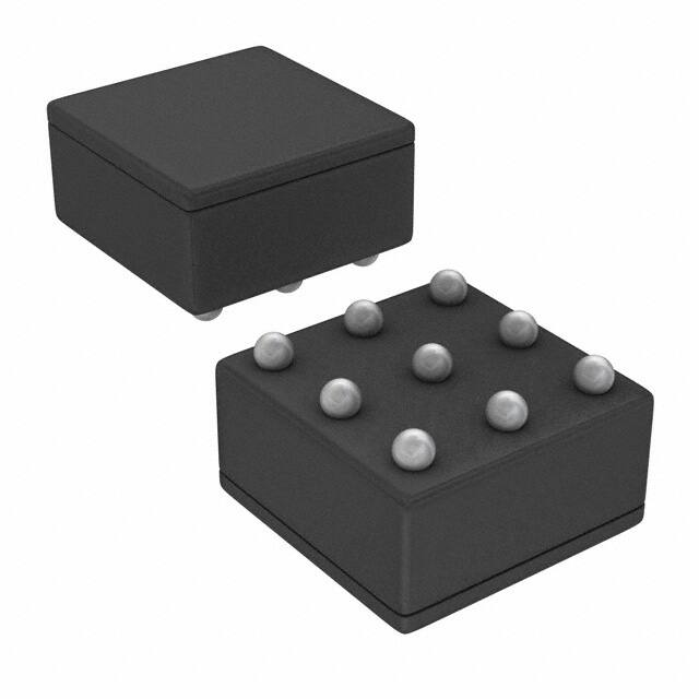
LM3710/LM3711 series are available in VSSOP-10
and 9-bump DSBGA packages.
1
2
•
•
•
•
•
•
•
•
•
•
•
Standard Reset Threshold Voltage: 3.08V
Custom Reset Threshold Voltages: For other
voltages between 2.2V and 5.0V in 10mV
increments, contact TI
No External Components Required
Manual-Reset Input
RESET (LM3710) or RESET (LM3711) Outputs
Precision Supply Voltage Monitor
Factory Programmable Reset and Watchdog
Timeout Delays
Separate Power Fail Comparator
Available in DSBGA Package for Minimum
Footprint
±0.5% Reset Threshold Accuracy at Room
Temperature
±2% Reset Threshold Accuracy Over
Temperature Extremes
Reset Assertion Down to 1V VCC (RESET
Option Only)
28 µA VCC Supply Current
APPLICATIONS
•
•
•
•
Built-in features include the following:
Reset: Reset is asserted during power-up, powerdown, and brownout conditions. RESET is ensured
down to VCC of 1.0V.
Manual Reset Input: An input that asserts reset when
pulled low.
Power-Fail Input: A 1.225V threshold detector for
power fail warning, or to monitor a power supply other
than VCC.
Low Line Output: This early power failure warning
indicator goes low when the supply voltage drops to a
value which is 2% higher than the reset threshold
voltage.
Watchdog Timer: The WDI (Watchdog Input)
monitors one of the µP's output lines for activity. If no
output transition occurs during the watchdog timeout
period, reset is activated.
Embedded Controllers and Processors
Intelligent Instruments
Automotive Systems
Critical µP Power Monitoring
Typical Application
VIN1
VCC
VIN2
VCC
PFI
Reset
WDI
PFO
NMI
LLO
INT
Reset
PP
MR
GND
bus
GND
1
2
Please be aware that an important notice concerning availability, standard warranty, and use in critical applications of
Texas Instruments semiconductor products and disclaimers thereto appears at the end of this data sheet.
All trademarks are the property of their respective owners.
PRODUCTION DATA information is current as of publication date.
Products conform to specifications per the terms of the Texas
Instruments standard warranty. Production processing does not
necessarily include testing of all parameters.
Copyright © 2000–2013, Texas Instruments Incorporated
�LM3710, LM3711
SNVS150E – NOVEMBER 2000 – REVISED MARCH 2013
www.ti.com
Connection Diagram
VCC 1
10
Reset
2
9
MR
NC
3
8
PFI
PFO
4
7
LLO
WDI
5
6
NC
GND
Figure 1. VSSOP-10
1
Reset
VCC
MR
PFO
NC
PFI
LLO
GND
2
3
C
B
WDI
A
Figure 2. Top View
(looking from the coating side)
DSBGA 9 Bump Package
PIN DESCRIPTIONS
Pin No.
2
DSBGA
VSSOP
A1
2
Name
Function
MR
Manual-Reset input. When MR is less than VMRT (Manual Reset Threshold) RESET/RESET is
engaged.
Power Supply input.
B1
1
VCC
C1
10
RESET
Reset Logic Output. Pulses low for tRP (Reset Timeout Period) when triggered, and stays low
whenever VCC is below the reset threshold or when MR is below VMRT. It remains low for tRP after
either VCC rises above the reset threshold, or after MR input rises above VMRT (LM3710 only).
RESET
Reset Logic Output. RESET is the inverse of RESET (LM3711 only).
C2
8
PFO
Power-Fail Logic Output. When PFI is below VPFT, PFO goes low; otherwise, PFO remains high.
C3
7
LLO
Low-Line Logic Output. Early Power-Fail warning output. Low when VCC falls below VLLOT (LowLine Output Threshold). This output can be used to generate an NMI (Non-Maskable Interrupt) to
provide an early warning of imminent power-failure.
B3
5
GND
Ground reference for all signals.
A3
4
WDI
Watchdog Input Transition Monitor: If no transition activity occurs for a period exceeding tWD
(Watchdog Timeout Period), reset is engaged.
A2
3
PFI
Power-Fail Comparator Input. When PFI is less than VPFT (Power-Fail Reset Threshold), the PFO
goes low; otherwise, PFO remains high.
B2
6, 9
NC
No Connect. Test input used at factory only. Leave floating.
Submit Documentation Feedback
Copyright © 2000–2013, Texas Instruments Incorporated
Product Folder Links: LM3710 LM3711
�LM3710, LM3711
www.ti.com
SNVS150E – NOVEMBER 2000 – REVISED MARCH 2013
Block Diagram
Table Of Functions
Part
Number
LM3710
LM3711
(1)
Active
Low
Reset
Active
High
Reset
Output
(X = totem-pole)
(Y = open-drain)
x
x
Reset
Timeout
Period
Watchdog
Timeout
Period
Manual
Reset
Power Fail
Comparator
Low Line
Output
X, Y (1)
Customized
Customized
x
x
x
X
Customized
Customized
x
x
x
Available upon request. Contact TI.
These devices have limited built-in ESD protection. The leads should be shorted together or the device placed in conductive foam
during storage or handling to prevent electrostatic damage to the MOS gates.
Submit Documentation Feedback
Copyright © 2000–2013, Texas Instruments Incorporated
Product Folder Links: LM3710 LM3711
3
�LM3710, LM3711
SNVS150E – NOVEMBER 2000 – REVISED MARCH 2013
www.ti.com
Absolute Maximum Ratings (1) (2)
−0.3V to 6.0V
Supply Voltage (VCC)
−0.3V to VCC + 0.3V
All Other Inputs
ESD Ratings (3)
Human Body Model
Machine Model
1.5kV
150V
(4)
Power Dissipation
(1)
(2)
(3)
(4)
Absolute Maximum Ratings indicate limits beyond which damage to the device may occur. Operating Ratings indicate conditions for
which the device is intended to be functional, but do not ensure specific performance limits. For ensured specifications and test
conditions, see the Electrical Characteristics. The ensured specifications apply only for the test conditions listed. Some performance
characteristics may degrade when the device is not operated under the listed conditions.
If Military/Aerospace specified devices are required, please contact the Texas Instruments Sales Office/Distributors for availability and
specifications.
The Human Body model is a 100 pF capacitor discharged through a 1.5 kΩ resistor into each pin. The machine model is a 200pF
capacitor discharged directly into each pin.
The maximum allowable power dissipation is a function of the maximum junction temperature, TJ(MAX), the junction-to-ambient thermal
resistance, θJ-A, and the ambient temperature, TA. The maximum allowable power dissipation at any ambient temperture is calculated
using:
Where the value of θJ-A for the VSSOP-10 package is 195°C/W in a typical PC board mounting and the DSBGA package is 220°C/W.
Operating Ratings (1)
−40°C ≤ TJ ≤ 85°C
Temperature Range
(1)
Absolute Maximum Ratings indicate limits beyond which damage to the device may occur. Operating Ratings indicate conditions for
which the device is intended to be functional, but do not ensure specific performance limits. For ensured specifications and test
conditions, see the Electrical Characteristics. The ensured specifications apply only for the test conditions listed. Some performance
characteristics may degrade when the device is not operated under the listed conditions.
LM3710/LM3711 Series Electrical Characteristics
Limits in the standard typeface are for TJ = 25°C and limits in boldface type apply over full operating range. Unless otherwise
specified: VCC = +2.2V to 5.5V.
Symbol
Parameter
Conditions
Min
Typ
Max
Units
POWER SUPPLY
VCC
ICC
Operating Voltage
Range: VCC
LM3710
1.0
5.5
LM3711
1.2
5.5
VCC Supply Current
All inputs = VCC; all outputs floating
V
28
50
µA
VRST
+0.5
+2
%
RESET THRESHOLD
VRST
Reset Threshold
−0.5
−2
VCC falling
−1.5
VCC falling: TA = 0°C to 70°C
VRSTH
tRP
tRD
Reset Threshold
Hysteresis
0.0032•VRST
Reset Timeout Period Reset
Reset
Reset
Reset
VCCto Reset Delay
+1.5
Timeout
Timeout
Timeout
Timeout
Period
Period
Period
Period
= E, J, N, S
= F, K, P, T
= G, L, Q, U
= H, M, R, V
1
20
140
1120
VCCfalling at 1mV/µs
1.4
28
200
1600
mV
2
40
280
2240
20
ms
µs
RESET (LM3711)
VOL
VOH
4
RESET
RESET
VCC > 2.25V, ISINK = 900µA
0.3
VCC > 2.7V, ISINK = 1.2mA
0.3
VCC > 4.5V, ISINK = 3.2mA
0.4
VCC > 1.2V, ISOURCE = 50µA
0.8 VCC
VCC > 1.8V, ISOURCE = 150µA
0.8 VCC
VCC > 2.25V, ISOURCE = 300µA
0.8 VCC
VCC > 2.7V, ISOURCE = 500µA
0.8 VCC
VCC > 4.5V, ISOURCE = 800µA
VCC − 1.5V
Submit Documentation Feedback
V
V
Copyright © 2000–2013, Texas Instruments Incorporated
Product Folder Links: LM3710 LM3711
�LM3710, LM3711
www.ti.com
SNVS150E – NOVEMBER 2000 – REVISED MARCH 2013
LM3710/LM3711 Series Electrical Characteristics (continued)
Limits in the standard typeface are for TJ = 25°C and limits in boldface type apply over full operating range. Unless otherwise
specified: VCC = +2.2V to 5.5V.
Symbol
ILKG
Parameter
Output Leakage
Current
Max
Units
VRESET = 5.5V
Conditions
Min
Typ
1.0
µA
VCC > 1.0V, ISINK = 50µA
0.3
VCC > 1.2V, ISINK = 100µA
0.3
VCC > 2.25V, ISINK = 900µA
0.3
VCC > 2.7V, ISINK = 1.2mA
0.3
VCC > 4.5V, ISINK = 3.2mA
0.4
RESET (LM3710)
VOL
VOH
RESET
RESET
VCC > 2.25V, ISOURCE = 300µA
V
0.8 VCC
VCC > 2.7V, ISOURCE = 500µA
0.8 VCC
VCC > 4.5V, ISOURCE = 800µA
VCC − 1.5V
WDI
WDI
Watchdog Input
Current
WDIT
Watchdog Input
Threshold
tWD
Watchdog Timeout
Period
−1
Watchdog
Watchdog
Watchdog
Watchdog
Timeout
Timeout
Timeout
Timeout
Period
Period
Period
Period
= E, F, G, H
= J, K, L, M
= N, P, Q, R
= S, T, U, V
+1
µA
0.2•VCC
1.225
0.8•VCC
V
4.3
71
1120
17900
6.2
102
1600
25600
9.3
153
2400
38400
ms
1.200
1.225
1.250
V
PFI/MR
VPFT
PFI Input Threshold
VMRT
MR Input Threshold
MR, Low
0.8
MR, High
VPFTH/
VMRTH
PFI/MR Threshold
Hysteresis
2.0
PFI/MR falling: VCC = VRST MAX to 5.5V
0.0032•VRST
IPFI
Input Current
(PFI only)
−75
RMR
MR Pull-up
Resistance
35
tMD
MR to Reset Delay
tMR
MR Pulse Width
56
V
mV
75
nA
75
kΩ
12
µS
25
µS
PFO, LLO
VOL
PFO, LLO Output
Voltage
VOH
VCC > 2.25V, ISINK = 900µA
0.3
VCC > 2.7V, ISINK = 1.2mA
0.3
VCC > 4.5V, ISINK = 3.2mA
0.4
VCC > 2.25V, ISOURCE = 300µA
0.8 VCC
VCC > 2.7V, ISOURCE = 500µA
0.8 VCC
VCC > 4.5V, ISOURCE = 800µA
VCC − 1.5V
V
LLO OUTPUT
VLLOT
LLO Output
Threshold
(VLLO − VRST, VCC
falling)
VLLOTH
Low-Line Comparator
Hysteresis
tCD
1.01•VRST
Low-Line Comparator VCC falling at 1mV/µs
Delay
1.02•VRST
1.03•VRST
0.0032•VRST
mV
20
µs
Submit Documentation Feedback
Copyright © 2000–2013, Texas Instruments Incorporated
Product Folder Links: LM3710 LM3711
V
5
�LM3710, LM3711
SNVS150E – NOVEMBER 2000 – REVISED MARCH 2013
www.ti.com
Typical Performance Characteristics
Supply Current vs Supply Voltage
3.3V Supply Current vs Temperature
30
30
29
Supply Current (PA)
Supply Current (PA)
25
20
15
10
27
26
25
24
5
0
1
28
2
3
4
Supply Voltage (V)
23
-40
5
0
25
70
Temperature (°C)
Figure 3.
Figure 4.
Normalized Reset Threshold Voltage vs Temperature
Reset Timeout Period vs VCC
220
0.4
215
0.3
Reset Timeout Period (ms)
Normalized Threshold Voltage (%)
0.5
0.2
0.1
0
-0.1
-0.2
-0.3
-0.4
-0.5
-40
25
Temperature (°C)
205
200
195
190
185
3.5
4
4.5
5
5.5
6
Supply Voltage (V)
Figure 5.
Figure 6.
Reset Timeout Period vs Temperature
Max. Transient Duration vs Reset Comparator Overdrive
(VCC = 3.3V)
80
Maximum Transient Duration (Ps)
Reset Timeout Period (ms)
210
180
3.0
85
215
210
205
200
195
190
-40
70
60
50
40
30
20
10
0
25
85
10
Temperature (°C)
100
1000
Reset Comparator Overdrive (mV)
VRST - VCC
Figure 7.
6
85
Figure 8.
Submit Documentation Feedback
Copyright © 2000–2013, Texas Instruments Incorporated
Product Folder Links: LM3710 LM3711
�LM3710, LM3711
www.ti.com
SNVS150E – NOVEMBER 2000 – REVISED MARCH 2013
Typical Performance Characteristics (continued)
Watchdog Timeout Period vs Temperature
(tWD programmed as 6.2ms)
Low-Line Comparator Propagation Delay vs Temperature
7
39
37
6.6
Propagation Delay (Ps)
Watchdog Timeout Period (ms)
6.8
6.4
6.2
6
5.8
5.6
5.4
35
33
31
29
27
5.2
5
-40
25
-40
85
25
R
Temperature ( C)
Figure 9.
-20
0
20
40
60
80
Temperature (oC)
Figure 10.
Submit Documentation Feedback
Copyright © 2000–2013, Texas Instruments Incorporated
Product Folder Links: LM3710 LM3711
7
�LM3710, LM3711
SNVS150E – NOVEMBER 2000 – REVISED MARCH 2013
www.ti.com
CIRCUIT INFORMATION
RESET OUTPUT
The Reset input of a µP initializes the device into a known state. The LM3710/LM3711 microprocessor
supervisory circuits assert a forced reset output to prevent code execution errors during power-up, power-down,
and brownout conditions.
RESET is ensured valid for VCC > 1V. Once VCC exceeds the reset threshold, an internal timer maintains the
output for the reset timeout period. After this interval, reset goes high. The LM3710 offers an active-low RESET;
The LM3711 offers an active-high RESET.
Any time VCC drops below the reset threshold (such as during a brownout), the reset activates. When VCC again
rises above the reset threshold, the internal timer starts. Reset holds until VCC exceeds the reset threshold for
longer than the reset timeout period. After this time, reset releases.
The Manual Reset input (MR) will initiate a forced reset also. See the MANUAL RESET INPUT (MR) section.
RESET THRESHOLD
The LM3710/LM3711 family is available with a reset voltage of 3.08V. Other reset thresholds in the 2.20V to
5.0V range, in steps of 10 mV, are available; contact Texas Instruments for details.
MANUAL RESET INPUT (MR)
Many µP-based products require a manual reset capability, allowing the operator to initiate a reset. The MR input
is fully debounced and provides an internal 56 kΩ pull-up. When the MR input is pulled below VMRT (1.225V) for
more than 25 µs, reset is asserted after a typical delay of 12 µs. Reset remains active as long as MR is held low,
and releases after the reset timeout period expires after MR rises above VMRT. Use MR with digital logic to assert
or to daisy chain supervisory circuits. It may be used as another low-line comparator by adding a buffer.
POWER-FAIL COMPARATOR (PFI/PFO)
The PFI is compared to a 1.225V internal reference, VPFT. If PFI is less than VPFT, the Power Fail Output PFO
drops low. The power-fail comparator signals a falling power supply, and is driven typically by an external voltage
divider that senses either the unregulated supply or another system supply voltage. The voltage divider generally
is chosen so the voltage at PFI drops below VPFT several milliseconds before the main supply voltage drops
below the reset threshold, providing advanced warning of a brownout.
The voltage threshold is set by R1 and R2 and is calculated as follows:
(1)
Note this comparator is completely separate from the rest of the circuitry, and may be employed for other
functions as needed.
LOW-LINE OUTPUT (LLO)
The low-line output comparator is typically used to provide a non-maskable interrupt to a µP when VCC begins
falling. LLO monitors VCC and goes low when VCC falls below VLLOT (typically 1.02 • VRST) with hysteresis of
0.0032 • VRST.
WATCHDOG TIMER INPUT (WDI)
The watchdog timer input monitors one of the microprocessor's output lines for activity. Each time a transition
occurs on this monitored line, the watchdog counter is reset. However, if no transition occurs and the timeout
period is reached, the LM3710/LM3711 assumes that the microprocessor has locked up and the reset output is
activated.
WDI is a high impedance input.
8
Submit Documentation Feedback
Copyright © 2000–2013, Texas Instruments Incorporated
Product Folder Links: LM3710 LM3711
�LM3710, LM3711
www.ti.com
SNVS150E – NOVEMBER 2000 – REVISED MARCH 2013
SPECIAL PRECAUTIONS FOR THE DSBGA PACKAGE
As with most integrated circuits, the LM3710 and LM3711 are sensitive to exposure from visible and infrared (IR)
light radiation. Unlike a plastic encapsulated IC, the DSBGA package has very limited shielding from light, and
some sensitivity to light reflected from the surface of the PC board or long wavelength IR entering the die from
the side may be experienced. This light could have an unpredictable affect on the electrical performance of the
IC. Care should be taken to shield the device from direct exposure to bright visible or IR light during operation.
DSBGA MOUNTING
The DSBGA package requires specific mounting techniques which are detailed in TI Application Note AN-1112
(SNVA009). Referring to the section Surface Mount Assembly Considerations, it should be noted that the pad
style which must be used with the 9-pin package is the NSMD (non-solder mask defined) type.
For best results during assembly, alignment ordinals on the PC board may be used to facilitate placement of the
DSBGA device.
Timing Diagrams
Figure 11. LM3710/LM3711 Reset Time with MR and WDI
Figure 12. LLO Output
Submit Documentation Feedback
Copyright © 2000–2013, Texas Instruments Incorporated
Product Folder Links: LM3710 LM3711
9
�LM3710, LM3711
SNVS150E – NOVEMBER 2000 – REVISED MARCH 2013
www.ti.com
Figure 13. PFI Comparator Timing Diagram
Typical Application Circuits
VIN2
VIN1
R1
VCC
RESET
RESET
PFI
PP
WDI
LLO
MR
PFO
GND
Active Data Line
Power-Fail Reset Threshold, VPFT = 1.225
GND
.( R
1
R2
+1
(
R2
INT
Figure 14. Monitoring Two Critical Supplies And Dataline
10
Submit Documentation Feedback
Copyright © 2000–2013, Texas Instruments Incorporated
Product Folder Links: LM3710 LM3711
�LM3710, LM3711
www.ti.com
SNVS150E – NOVEMBER 2000 – REVISED MARCH 2013
1.8V
3.3V
107k
VI/O
VCC
PFI
332k
Vcore
RESET
RESET
WDI
PFO
MR
GND
3.3k
Active Data Line
Figure 15. Monitoring Two Supplies plus Manual Reset And Dataline
1.8
V
3.3V
107k
VCC
VI/O
RESET
PFI
VCORE
RESET
332k
WDI
MR
PFO
GND
Active Data Line
FAULT
(Normally High)
Figure 16. Monitoring Dual Supplies plus External Fault Input And Dataline
Raw Supply
(Battery)
System
Regulator
3.3V
0.1P ceramic
R1
VCC
INT
PFO
PFI
PP
WDI
R2
MR
RESET
RESET
GND
Active Data
Line
.( R
1
R2
+1
(
Power-Fail Reset Threshold, VPFT = 1.225
Note: MR input with its 1.225V nominal threshold, may monitor an additional supply voltage. An internal 56 kΩ pull-up
resistor is included on this input.
Figure 17. Microprocessor Supervisor with Early Warning Detector
Submit Documentation Feedback
Copyright © 2000–2013, Texas Instruments Incorporated
Product Folder Links: LM3710 LM3711
11
�LM3710, LM3711
SNVS150E – NOVEMBER 2000 – REVISED MARCH 2013
www.ti.com
+3.3 to 5V
VCC
PFI
RESET
OUTPUT
WDI
tWD
GND
tRP
Period = tRP + tWD
Figure 18. LM3710 Long Period oscillator
12
Submit Documentation Feedback
Copyright © 2000–2013, Texas Instruments Incorporated
Product Folder Links: LM3710 LM3711
�LM3710, LM3711
www.ti.com
SNVS150E – NOVEMBER 2000 – REVISED MARCH 2013
REVISION HISTORY
Changes from Revision D (March 2013) to Revision E
•
Page
Changed layout of National Data Sheet to TI format .......................................................................................................... 12
Submit Documentation Feedback
Copyright © 2000–2013, Texas Instruments Incorporated
Product Folder Links: LM3710 LM3711
13
�PACKAGE OPTION ADDENDUM
www.ti.com
10-Dec-2020
PACKAGING INFORMATION
Orderable Device
Status
(1)
Package Type Package Pins Package
Drawing
Qty
Eco Plan
(2)
Lead finish/
Ball material
MSL Peak Temp
Op Temp (°C)
Device Marking
(3)
(4/5)
(6)
LM3710XKMM-463/NOPB
ACTIVE
VSSOP
DGS
10
1000
RoHS & Green
SN
Level-1-260C-UNLIM
LM3710XQMM-308/NOPB
ACTIVE
VSSOP
DGS
10
1000
RoHS & Green
SN
Level-1-260C-UNLIM
LM3710YQMM-232/NOPB
ACTIVE
VSSOP
DGS
10
1000
RoHS & Green
SN
Level-1-260C-UNLIM
R74B
-40 to 85
R37B
R77B
(1)
The marketing status values are defined as follows:
ACTIVE: Product device recommended for new designs.
LIFEBUY: TI has announced that the device will be discontinued, and a lifetime-buy period is in effect.
NRND: Not recommended for new designs. Device is in production to support existing customers, but TI does not recommend using this part in a new design.
PREVIEW: Device has been announced but is not in production. Samples may or may not be available.
OBSOLETE: TI has discontinued the production of the device.
(2)
RoHS: TI defines "RoHS" to mean semiconductor products that are compliant with the current EU RoHS requirements for all 10 RoHS substances, including the requirement that RoHS substance
do not exceed 0.1% by weight in homogeneous materials. Where designed to be soldered at high temperatures, "RoHS" products are suitable for use in specified lead-free processes. TI may
reference these types of products as "Pb-Free".
RoHS Exempt: TI defines "RoHS Exempt" to mean products that contain lead but are compliant with EU RoHS pursuant to a specific EU RoHS exemption.
Green: TI defines "Green" to mean the content of Chlorine (Cl) and Bromine (Br) based flame retardants meet JS709B low halogen requirements of


 工商网监
湘ICP备2023018690号
工商网监
湘ICP备2023018690号
