User's Guide
SNVA322C – January 2008 – Revised May 2013
AN-1785 LM3881 Power Sequencer Evaluation Board
1
Introduction
The LM3881 evaluation board has been designed to permit the designer to connect it directly to the
Enable or Remote ON/OFF pins of power supply devices of an existing system to facilitate system
sequencing. The block diagram of a typical system application is given in Figure 1.
Upon enabling the device, the three open drain output flags will rise in sequential order, 1-2-3. Once the
part is disabled, the shutdown sequence will occur in reverse order 3-2-1. Therefore the last power supply
that started up will be the first to shutdown.
DEVICE 1
Input
Supply
LM3881
EN
VCC
Enable
EN
DEVICE 2
FLAG1
FLAG2
Invert
INV
EN
FLAG3
GND
DEVICE 3
EN
Figure 1. Typical System Application Using LM3881 Sequencer
All trademarks are the property of their respective owners.
SNVA322C – January 2008 – Revised May 2013
Submit Documentation Feedback
AN-1785 LM3881 Power Sequencer Evaluation Board
Copyright © 2008–2013, Texas Instruments Incorporated
1
�Timing Sequence
2
www.ti.com
Timing Sequence
Figure 2 and Figure 3 present the power up and power down timing sequence of the output flags with the
INV at logic level low and high, respectively. The waveform labeled TADJ refers to the voltage on the
timer adjust pin of the LM3881.
(a)
(b)
EN
EN
FLAG1
FLAG1
FLAG2
FLAG2
FLAG3
FLAG3
TADJ
TADJ
TD1
TD2
TD3
TD1
TD2
TD3
9 Clock
Cycles
8 Clock
Cycles
8 Clock
Cycles
9 Clock
Cycles
8 Clock
Cycles
8 Clock
Cycles
Figure 2. Power Up Sequence (a) INV Low, (b) INV High
(a)
(b)
EN
EN
FLAG1
FLAG1
FLAG2
FLAG2
FLAG3
FLAG3
TADJ
TADJ
TD4
9 Clock
Cycles
TD5
TD6
TD4
TD5
TD6
8 Clock
Cycles
8 Clock
Cycles
9 Clock
Cycles
8 Clock
Cycles
8 Clock
Cycles
Figure 3. Power Down Sequence (a) INV Low, (b) INV High
3
LM3881 Circuit Schematic
The evaluation board schematic is given in Figure 4. The board contains the LM3881MFX device which
has a timing capacitor, CADJ, of 10 nF so that each time delay between flags will be approximately 10 ms.
The pull-up resistors of the flag outputs (R1, R2, R3) are each 100 kΩ.
The LM3881 has an enable pin that is pulled up by an internal 7 µA current source. Thus, the associated
PCB terminal, labeled EN, can be left open circuit if desired. In this case, the flags will release when the
LM3881 VCC supply exceeds its UVLO level. Finally, the LM3881 has an invert pin that sets the polarity of
the flags. The associated PCB terminal, labeled INV, needs to be connected to VCC or GND.
The evaluation board bill of materials, LM3881 pin-out and pin description are given in Table 1, Figure 5
and Table 2 respectively.
2
AN-1785 LM3881 Power Sequencer Evaluation Board
SNVA322C – January 2008 – Revised May 2013
Submit Documentation Feedback
Copyright © 2008–2013, Texas Instruments Incorporated
�LM3881 Evaluation Board Bill of Materials (BOM)
www.ti.com
Input Supply
(2.7V ± 5.5V)
R3
U1
R2
R1
LM3881
VCC
ENable Input
EN
INVert Input
INV
FLAG1
Flag 1
FLAG2
Flag 2
FLAG3
Flag 3
TADJ
CADJ
GND
Figure 4. LM3881 Schematic
4
LM3881 Evaluation Board Bill of Materials (BOM)
Table 1. Evaluation Board Bill of Materials
5
Ref Des
Description
Case Size
Manufacturer
Manufacturer P/N
U1
LM3881 Sequencer
MSOP-8
Texas Instruments
LM388
R1
100 kΩ
0603
Vishay Dale
CRCW06031003F-e3
R2
100 kΩ
0603
Vishay Dale
CRCW06031003F-e3
R3
100 kΩ
0603
Vishay Dale
CRCW06031003F-e3
CADJ
10 nF ±10% X7R 16 V
0603
Murata
GRM188R71C103KA01
LM3881 Pin-Out
VCC
EN
GND
INV
1
8
2
7
3
4
FLAG1
LM3881
6
5
FLAG2
FLAG3
TADJ
Figure 5. LM3881 Pin-Out
SNVA322C – January 2008 – Revised May 2013
Submit Documentation Feedback
AN-1785 LM3881 Power Sequencer Evaluation Board
Copyright © 2008–2013, Texas Instruments Incorporated
3
�LM3881 Pin Descriptions
6
www.ti.com
LM3881 Pin Descriptions
Table 2. Pin Descriptions
7
Pin No
Name
Function
1
VCC
Input Supply
2
EN
Precision Enable
3
GND
Ground
4
INV
Output Logic Invert
5
TADJ
Timer Adjust
6
FLAG3
Open Drain Output #3
7
FLAG2
Open Drain Output #2
8
FLAG1
Open Drain Output #1
PC Board Layout
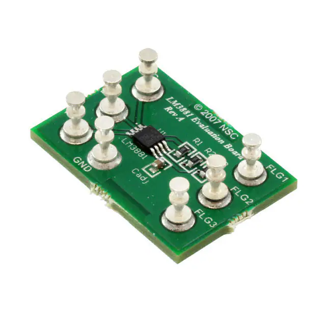
The evaluation board is based on a small 1.09” x 0.76” FR4 PCB with two layers of copper. The actual
layout can be seen in Figure 6 and Figure 7. When looking at the top layer, pin 1 of the LM3881 is on the
upper left. An optional component, assigned reference designator R4, is placed on the bottom side of the
PCB to facilitate connection of INV to GND.
Figure 6. Top Side PCB Layout
4
AN-1785 LM3881 Power Sequencer Evaluation Board
SNVA322C – January 2008 – Revised May 2013
Submit Documentation Feedback
Copyright © 2008–2013, Texas Instruments Incorporated
�PC Board Layout
www.ti.com
Figure 7. Bottom Side PCB Layout
SNVA322C – January 2008 – Revised May 2013
Submit Documentation Feedback
AN-1785 LM3881 Power Sequencer Evaluation Board
Copyright © 2008–2013, Texas Instruments Incorporated
5
�IMPORTANT NOTICE
Texas Instruments Incorporated and its subsidiaries (TI) reserve the right to make corrections, enhancements, improvements and other
changes to its semiconductor products and services per JESD46, latest issue, and to discontinue any product or service per JESD48, latest
issue. Buyers should obtain the latest relevant information before placing orders and should verify that such information is current and
complete. All semiconductor products (also referred to herein as “components”) are sold subject to TI’s terms and conditions of sale
supplied at the time of order acknowledgment.
TI warrants performance of its components to the specifications applicable at the time of sale, in accordance with the warranty in TI’s terms
and conditions of sale of semiconductor products. Testing and other quality control techniques are used to the extent TI deems necessary
to support this warranty. Except where mandated by applicable law, testing of all parameters of each component is not necessarily
performed.
TI assumes no liability for applications assistance or the design of Buyers’ products. Buyers are responsible for their products and
applications using TI components. To minimize the risks associated with Buyers’ products and applications, Buyers should provide
adequate design and operating safeguards.
TI does not warrant or represent that any license, either express or implied, is granted under any patent right, copyright, mask work right, or
other intellectual property right relating to any combination, machine, or process in which TI components or services are used. Information
published by TI regarding third-party products or services does not constitute a license to use such products or services or a warranty or
endorsement thereof. Use of such information may require a license from a third party under the patents or other intellectual property of the
third party, or a license from TI under the patents or other intellectual property of TI.
Reproduction of significant portions of TI information in TI data books or data sheets is permissible only if reproduction is without alteration
and is accompanied by all associated warranties, conditions, limitations, and notices. TI is not responsible or liable for such altered
documentation. Information of third parties may be subject to additional restrictions.
Resale of TI components or services with statements different from or beyond the parameters stated by TI for that component or service
voids all express and any implied warranties for the associated TI component or service and is an unfair and deceptive business practice.
TI is not responsible or liable for any such statements.
Buyer acknowledges and agrees that it is solely responsible for compliance with all legal, regulatory and safety-related requirements
concerning its products, and any use of TI components in its applications, notwithstanding any applications-related information or support
that may be provided by TI. Buyer represents and agrees that it has all the necessary expertise to create and implement safeguards which
anticipate dangerous consequences of failures, monitor failures and their consequences, lessen the likelihood of failures that might cause
harm and take appropriate remedial actions. Buyer will fully indemnify TI and its representatives against any damages arising out of the use
of any TI components in safety-critical applications.
In some cases, TI components may be promoted specifically to facilitate safety-related applications. With such components, TI’s goal is to
help enable customers to design and create their own end-product solutions that meet applicable functional safety standards and
requirements. Nonetheless, such components are subject to these terms.
No TI components are authorized for use in FDA Class III (or similar life-critical medical equipment) unless authorized officers of the parties
have executed a special agreement specifically governing such use.
Only those TI components which TI has specifically designated as military grade or “enhanced plastic” are designed and intended for use in
military/aerospace applications or environments. Buyer acknowledges and agrees that any military or aerospace use of TI components
which have not been so designated is solely at the Buyer's risk, and that Buyer is solely responsible for compliance with all legal and
regulatory requirements in connection with such use.
TI has specifically designated certain components as meeting ISO/TS16949 requirements, mainly for automotive use. In any case of use of
non-designated products, TI will not be responsible for any failure to meet ISO/TS16949.
Products
Applications
Audio
www.ti.com/audio
Automotive and Transportation
www.ti.com/automotive
Amplifiers
amplifier.ti.com
Communications and Telecom
www.ti.com/communications
Data Converters
dataconverter.ti.com
Computers and Peripherals
www.ti.com/computers
DLP® Products
www.dlp.com
Consumer Electronics
www.ti.com/consumer-apps
DSP
dsp.ti.com
Energy and Lighting
www.ti.com/energy
Clocks and Timers
www.ti.com/clocks
Industrial
www.ti.com/industrial
Interface
interface.ti.com
Medical
www.ti.com/medical
Logic
logic.ti.com
Security
www.ti.com/security
Power Mgmt
power.ti.com
Space, Avionics and Defense
www.ti.com/space-avionics-defense
Microcontrollers
microcontroller.ti.com
Video and Imaging
www.ti.com/video
RFID
www.ti-rfid.com
OMAP Applications Processors
www.ti.com/omap
TI E2E Community
e2e.ti.com
Wireless Connectivity
www.ti.com/wirelessconnectivity
Mailing Address: Texas Instruments, Post Office Box 655303, Dallas, Texas 75265
Copyright © 2013, Texas Instruments Incorporated
�