Order
Now
Product
Folder
Support &
Community
Tools &
Software
Technical
Documents
Reference
Design
LM393B, LM2903B, LM193, LM293, LM293A, LM393, LM393A, LM2903, LM2903V
SLCS005AC – OCTOBER 1979 – REVISED FEBRUARY 2020
LM393B, LM2903B, LM193, LM293, LM393 and LM2903 Dual Comparators
1 Features
3 Description
•
•
The LM393B and LM2903B devices are the next
generation versions of the industry-standard LM393
and LM2903 comparator family. These next
generation
B-version
comparators
provide
outstanding value for cost-sensitive applications
featuring lower offset voltage, higher supply voltage
capability, lower supply current, lower input bias
current, lower propagation delay, and improved 2 kV
ESD performance and input ruggedness through
dedicated ESD clamps. The LM393B and LM2903B
can drop-in replace the LM293, LM393 and LM2903,
for both "A" and "V" grades.
1
•
•
•
•
•
NEW LM393B and LM2903B
Improved specifications of B-version
– Maximum rating: up to 38 V
– ESD rating (HBM): 2k V
– Low input offset: 0.37 mV
– Low input bias current: 3.5 nA
– Low supply-current: 200 µA per comparator
– Faster response time of 1 µsec
– Extended temperature range for LM393B
– Available in tiny 2 x 2mm WSON package
B-version is drop-in replacement for LM293,
LM393 and LM2903, A and V versions
Common-mode input voltage range includes
ground
Differential input voltage range equal to maximumrated supply voltage: ±38 V
Low output saturation voltage
Output compatible with TTL, MOS, and CMOS
2 Applications
•
•
•
•
•
•
•
•
•
•
Vacuum robot
Single phase UPS
Server PSU
Cordless power tool
Wireless Infrastructure
Applicances
Building Automation
Factory automation & control
Motor drives
Infotainment & cluster
All devices consist of two independent voltage
comparators that are designed to operate from a
single power supply over a wide range of voltages.
Quiescent current is independent of the supply
voltage, and the outputs can be connected to other
open-collector outputs to achieve wired-AND
relationships.
Device Information(1)
PART NUMBER
PACKAGE
BODY SIZE (NOM)
LM393B, LM2903B, LM193,
LM293, LM293A, LM393,
LM393A, LM2903,
LM2903V, LM2903AV
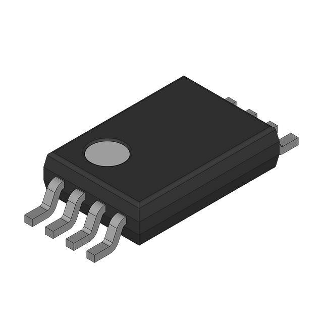
SOIC (8)
4.90 mm x 3.91 mm
LM393B, LM2903B, LM293,
LM293A, LM393, LM393A,
LM2903
VSSOP (8)
3.00 mm x 3.00 mm
LM293, LM393, LM393A,
LM2903
PDIP (8)
9.81 mm × 6.35 mm
LM393, LM393A, LM2903
SO (8)
6.20 mm x 5.30 mm
LM393B, LM2903B, LM393,
LM393A, LM2903,
LM2903V, LM2903AV
TSSOP (8)
3.00 mm x 4.40 mm
LM393B
SOT-23 (8) 2.90 mm x 1.60 mm
LM393B, LM2903B
WSON (8)
2.00 mm × 2.00 mm
(1) For all available packages, see the orderable addendum at
the end of the data sheet.
Family Comparison Table
LM393B
LM2903B
LM393
LM393A
LM2903
LM2903V
LM2903AV
LM193
LM293
LM293A
Units
3 to 36
3 to 36
2 to 30
2 to 30
2 to 32
2 to 30
2 to 30
V
Total Supply Current
(5V to 36V max)
0.6 to 0.8
0.6 to 0.8
1 to 2.5
1 to 2.5
1 to 2.5
1 to 2.5
1 to 2.5
mA
Temperature Range
−40 to 85
−40 to 125
0 to 70
−40 to 125
−40 to 125
−55 to 125
−25 to 85
°C
2000
2000
1000
1000
1000
1000
1000
V
±4
±4
±9
±4
± 15
± 15
±4
±9
±9
±4
V
3.5 / 25
3.5 / 25
25 / 250
25 / 250
25 / 250
25 / 100
25 / 250
nA
1
1
1.3
1.3
1.3
1.3
1.3
µsec
Specification
Supply Votlage
ESD (HBM)
Offset Voltage
(Max over temp)
Input Bias Current (typ / max)
Response Time (typ)
1
An IMPORTANT NOTICE at the end of this data sheet addresses availability, warranty, changes, use in safety-critical applications,
intellectual property matters and other important disclaimers. PRODUCTION DATA.
�LM393B, LM2903B, LM193, LM293, LM293A, LM393, LM393A, LM2903, LM2903V
SLCS005AC – OCTOBER 1979 – REVISED FEBRUARY 2020
www.ti.com
Table of Contents
1
2
3
4
5
6
Features ..................................................................
Applications ...........................................................
Description .............................................................
Revision History.....................................................
Pin Configuration and Functions .........................
Specifications.........................................................
1
1
1
2
3
4
6.1
6.2
6.3
6.4
6.5
Absolute Maximum Ratings ...................................... 4
ESD Ratings.............................................................. 4
Recommended Operating Conditions....................... 4
Thermal Information: LM193 ..................................... 5
Thermal Information: LM293, LM393, LM2903 (all 'V'
and 'A' suffixes).......................................................... 5
6.6 Thermal Information: LM393B and LM2903B ........... 5
6.7 Electrical Characteristics LM393B ............................ 6
6.8 Electrical Characteristics LM2903B .......................... 7
6.9 Switching Characteristics LM393B and LM2903B .... 7
6.10 Electrical Characteristics for LM193, LM293, and
LM393 (without A suffix) ............................................ 8
6.11 Electrical Characteristics for LM293A and
LM393A...................................................................... 9
6.12 Electrical Characteristics for LM2903, LM2903V,
and LM2903AV ........................................................ 10
6.13 Switching Characteristics: LM193, LM239, LM393,
LM2903, all 'A' and 'V' versions ............................... 10
6.14 Typical Characteristics, LMx93, LM2903 (all 'V' and
'A' suffixes) .............................................................. 11
6.15 Typical Characteristics, LM393B and LM2903B ... 12
7
Detailed Description ............................................ 18
7.1
7.2
7.3
7.4
8
Overview .................................................................
Functional Block Diagram .......................................
Feature Description.................................................
Device Functional Modes........................................
18
18
18
18
Application and Implementation ........................ 19
8.1 Application Information............................................ 19
8.2 Typical Application ................................................. 19
9 Power Supply Recommendations...................... 22
10 Layout................................................................... 22
10.1 Layout Guidelines ................................................. 22
10.2 Layout Example .................................................... 22
11 Device and Documentation Support ................. 23
11.1
11.2
11.3
11.4
11.5
11.6
Related Links ........................................................
Receiving Notification of Documentation Updates
Support Resources ...............................................
Trademarks ...........................................................
Electrostatic Discharge Caution ............................
Glossary ................................................................
23
23
23
23
23
23
12 Mechanical, Packaging, and Orderable
Information ........................................................... 23
4 Revision History
NOTE: Page numbers for previous revisions may differ from page numbers in the current version.
Changes from Revision AB (December 2019) to Revision AC
Page
•
Changed front page Features, Applications and Description text to highlight B version. ...................................................... 1
•
Added WSON and SOT-23-8 packages................................................................................................................................. 1
•
Added Links to Family Table ................................................................................................................................................. 1
•
Added DDF and DSG pkgs to Thermal Table ........................................................................................................................ 5
Changes from Revision AA (September 2019) to Revision AB
Page
•
Changed LM393B and LM2903B from Preview to Active status ........................................................................................... 1
•
Added Family Comparison Table ........................................................................................................................................... 1
Changes from Revision Z (October 2017) to Revision AA
Page
•
Added "B" devices with various text changes throughout datasheet. .................................................................................... 1
•
Deleted from Device Information old LM193 CDIP and LCCC package references and drawings. These are on the
LM139-MIL datasheet............................................................................................................................................................. 1
•
Added "B" devices Thermal Information table. ....................................................................................................................... 5
•
Added "B" device electrical tables .......................................................................................................................................... 6
•
Added "B" device graphs ..................................................................................................................................................... 12
2
Submit Documentation Feedback
Copyright © 1979–2020, Texas Instruments Incorporated
Product Folder Links: LM393B LM2903B LM193 LM293 LM293A LM393 LM393A LM2903 LM2903V
�LM393B, LM2903B, LM193, LM293, LM293A, LM393, LM393A, LM2903, LM2903V
www.ti.com
SLCS005AC – OCTOBER 1979 – REVISED FEBRUARY 2020
5 Pin Configuration and Functions
D, DGK, JG, P, PS, DDF or PW Package
8-Pin SOIC, VSSOP, PDIP, SO, or TSSOP
Top View
1OUT
1IN−
1IN+
GND
1
8
2
7
3
6
4
5
VCC
2OUT
2IN−
2IN+
DSG Package
8-Pin WSON With Exposed Pad
Top View
1OUT
1
1IN±
2
1IN+
3
GND
4
Exposed
Thermal
Die Pad
on
Underside
8
V+
7
2OUT
6
2IN±
5
2IN+
Connect thermal pad directly to GND pin.
Pin Functions
PIN
NAME
SOIC, VSSOP,
PDIP, SO, DDF and
TSSOP
DSG
1OUT
1
1
Output
1IN–
2
2
Input
Negative input pin of comparator 1
1IN+
3
3
Input
Positive input pin of comparator 1
GND
4
4
—
2IN+
5
5
Input
Positive input pin of comparator 2
2IN-
6
6
Input
Negative input pin of comparator 2
2OUT
7
7
Output
VCC
8
8
—
Positive Supply
Thermal
Pad
—
PAD
—
Connect directly to GND pin
Copyright © 1979–2020, Texas Instruments Incorporated
I/O
DESCRIPTION
Output pin of comparator 1
Ground
Output pin of comparator 2
Submit Documentation Feedback
Product Folder Links: LM393B LM2903B LM193 LM293 LM293A LM393 LM393A LM2903 LM2903V
3
�LM393B, LM2903B, LM193, LM293, LM293A, LM393, LM393A, LM2903, LM2903V
SLCS005AC – OCTOBER 1979 – REVISED FEBRUARY 2020
www.ti.com
6 Specifications
6.1 Absolute Maximum Ratings
over operating free-air temperature range (unless otherwise noted)
(1)
MIN
VCC
Supply voltage (2)
VID
Differential input voltage (3)
VI
Input voltage (either input)
IIK
Input current (4)
Non-B Versions
38
V
36
–0.3
V
38
-50
IO
Output current
ISC
Duration of output short circuit to ground (5)
TJ
Operating virtual-junction temperature
Tstg
Storage temperature
(5)
36
-38
Non-B Versions
Output voltage
(2)
(3)
(4)
-36
B Versions Only
B Versions Only
V
38
Non-B Versions
Non-B Versions
UNIT
36
–0.3
B Versions Only
VO
(1)
MAX
–0.3
B Versions Only
mA
36
V
38
Non-B Versions
20
B Versions Only
25
mA
Unlimited
–65
150
°C
150
°C
Stresses beyond those listed under Absolute Maximum Ratings may cause permanent damage to the device. These are stress ratings
only, and functional operation of the device at these or any other conditions beyond those indicated under Recommended Operating
Conditions is not implied. Exposure to absolute-maximum-rated conditions for extended periods may affect device reliability. Production
Processing Does Not Necessarily Include Testing of All Parameters.
All voltage values, except differential voltages, are with respect to network ground.
Differential voltages are at IN+ with respect to IN–.
Input current flows thorough parasitic diode to ground and turns on parasitic transistors that increases ICC and may cause output to be
incorrect. Normal operation resumes when input current is removed.
Short circuits from outputs to VCC can cause excessive heating and eventual destruction.
6.2 ESD Ratings
VALUE
UNIT
LM393B and LM2903B Only
V(ESD)
Electrostatic discharge
Human body model (HBM), per ANSI/ESDA/JEDEC JS-001 (1)
±2000
Charged-device model (CDM), per JEDEC specification JESD22-C101 (2)
±1000
Human body model (HBM), per ANSI/ESDA/JEDEC JS-001 (1)
±1000
Charged-device model (CDM), per JEDEC specification JESD22-C101 (2)
±750
V
All Other Versions
V(ESD)
(1)
(2)
Electrostatic discharge
V
JEDEC document JEP155 states that 500-V HBM allows safe manufacturing with a standard ESD control process.
JEDEC document JEP157 states that 250-V CDM allows safe manufacturing with a standard ESD control process.
6.3 Recommended Operating Conditions
Over operating free-air temperature range (unless otherwise noted)
Supply voltage, VS = (V+) – (V–)
Input voltage range, VIVR
Ambient temperature, TA
4
Submit Documentation Feedback
MIN
MAX
non-V devices
2
30
V devices
2
32
"B" version devices
3
36
non-B devices
0
(V+) – 2.0
"B" version devices
–0.1
LM193
–55
125
LM2903, LM2903V, LM2903AV, LM2903B
–40
125
LM393B
–40
85
LM293, LM293A
–25
85
LM393, LM393A
0
70
UNIT
V
V
°C
Copyright © 1979–2020, Texas Instruments Incorporated
Product Folder Links: LM393B LM2903B LM193 LM293 LM293A LM393 LM393A LM2903 LM2903V
�LM393B, LM2903B, LM193, LM293, LM293A, LM393, LM393A, LM2903, LM2903V
www.ti.com
SLCS005AC – OCTOBER 1979 – REVISED FEBRUARY 2020
6.4 Thermal Information: LM193
LM193
D
(SOIC)
THERMAL METRIC (1)
UNIT
8 pin
RθJA
Junction-to-ambient thermal resistance
126.4
°C/W
RθJC(top)
RθJB
Junction-to-case (top) thermal resistance
70
°C/W
Junction-to-board thermal resistance
64.9
°C/W
ψJT
Junction-to-top characterization parameter
20.3
°C/W
ψJB
Junction-to-board characterization parameter
64.5
°C/W
RθJC(bot)
Junction-to-case (bottom) thermal resistance
n/a
°C/W
(1)
For more information about traditional and new thermal metrics, see the Semiconductor and IC Package Thermal Metrics application
report.
6.5 Thermal Information: LM293, LM393, LM2903 (all 'V' and 'A' suffixes)
LM293, LM393, LM2903
THERMAL METRIC
D
(SOIC)
(1)
DGK
(VSSOP)
P
(PDIP)
PS
(SO)
PW
(TSSOP)
UNIT
8 pin
8 pin
8 pin
8 pin
8 pin
RθJA
Junction-to-ambient thermal resistance
131.8
199.4
73.7
139
194.1
°C/W
RθJC(top)
Junction-to-case (top) thermal resistance
78.4
90.2
62.6
98.9
77.0
°C/W
RθJB
Junction-to-board thermal resistance
72.2
120.8
50.8
83.7
123.0
°C/W
ψJT
Junction-to-top characterization parameter
26.5
21.5
39.2
47.4
13.1
°C/W
ψJB
Junction-to-board characterization parameter
71.1
119.1
50.7
83
121.3
°C/W
(1)
For more information about traditional and new thermal metrics, see the Semiconductor and IC Package Thermal Metrics application
report.
6.6 Thermal Information: LM393B and LM2903B
LM393B, LM2903B
THERMAL METRIC (1)
D
(SOIC)
PW
(TSSOP)
DGK
(VSSOP)
DDF
(SOT-23)
DSG
(WSON)
8 pins
UNIT
8 pin
8 pin
8 pin
8 pin
RθJA
Junction-to-ambient thermal resistance
148.5
200.6
193.7
197.9
96.9
°C/W
RθJC(top)
Junction-to-case (top) thermal resistance
90.2
89.6
82.9
119.2
119.0
°C/W
RθJB
Junction-to-board thermal resistance
91.8
131.3
115.5
115.4
63.1
°C/W
ψJT
Junction-to-top characterization parameter
38.5
22.1
20.8
19.4
12.4
°C/W
ψJB
Junction-to-board characterization parameter
91.1
129.6
113.9
113.7
63.0
°C/W
RθJC(bot)
Junction-to-case (bottom) thermal resistance
-
-
-
-
37.8
°C/W
(1)
For more information about traditional and new thermal metrics, see the Semiconductor and IC Package Thermal Metrics application
report.
Copyright © 1979–2020, Texas Instruments Incorporated
Submit Documentation Feedback
Product Folder Links: LM393B LM2903B LM193 LM293 LM293A LM393 LM393A LM2903 LM2903V
5
�LM393B, LM2903B, LM193, LM293, LM293A, LM393, LM393A, LM2903, LM2903V
SLCS005AC – OCTOBER 1979 – REVISED FEBRUARY 2020
www.ti.com
6.7 Electrical Characteristics LM393B
VS = 5 V, VCM = (V–) ; TA = 25°C (unless otherwise noted).
PARAMETER
VIO
Input offset voltage
IB
Input bias current
TEST CONDITIONS
VS = 5 to 36V
VS = 5 to 36V, TA = –40°C to +85°C
MIN
TYP
MAX
–2.5
±0.37
2.5
–4
4
–3.5
UNIT
mV
–25
nA
–50
nA
10
nA
–25
25
nA
TA = –40°C to +85°C
–10
±0.5
IOS
Input offset current
VCM
Common mode range
VS = 3 to 36V
(V–)
(V+) – 1.5
V
VCM
Common mode range
VS = 3 to 36V, TA = –40°C to +85°C
(V–)
(V+) – 2.0
V
AVD
Large signal differential voltage
amplification
VS = 15V, VO = 1.4V to 11.4V;
RL ≥ 15k to (V+)
VOL
Low level output Voltage {swing
from (V–)}
IOH-LKG
High-level output leakage current
IOL
Low level output current
VOL = 1.5V; VID = -1V; VS = 5V
IQ
Quiescent current (all
comparators)
VS = 5 V, no load
400
600
µA
VS = 36 V, no load, TA = –40°C to +85°C
550
800
µA
6
Submit Documentation Feedback
TA = –40°C to +85°C
50
ISINK ≤ 4mA, VID = -1V
200
110
ISINK ≤ 4mA, VID = -1V
TA = –40°C to +85°C
V/mV
400
mV
550
mV
nA
(V+) = VO = 5 V; VID = 1V
0.1
20
(V+) = VO = 36V; VID = 1V
0.3
50
6
21
nA
mA
Copyright © 1979–2020, Texas Instruments Incorporated
Product Folder Links: LM393B LM2903B LM193 LM293 LM293A LM393 LM393A LM2903 LM2903V
�LM393B, LM2903B, LM193, LM293, LM293A, LM393, LM393A, LM2903, LM2903V
www.ti.com
SLCS005AC – OCTOBER 1979 – REVISED FEBRUARY 2020
6.8 Electrical Characteristics LM2903B
VS = 5 V, VCM = (V–) ; TA = 25°C (unless otherwise noted).
PARAMETER
VIO
Input offset voltage
IB
Input bias current
IOS
Input offset current
VCM
Common mode range
TEST CONDITIONS
VS = 5 to 36V
VS = 5 to 36V, TA = –40°C to +125°C
MIN
TYP
MAX
–2.5
±0.37
2.5
–4
4
–3.5
UNIT
mV
–25
nA
–50
nA
10
nA
–25
25
nA
VS = 3 to 36V
(V–)
(V+) – 1.5
V
VS = 3 to 36V, TA = –40°C to +125°C
(V–)
(V+) – 2.0
V
TA = –40°C to +125°C
–10
TA = –40°C to +125°C
VS = 15V, VO = 1.4V to 11.4V;
RL ≥ 15k to (V+)
±0.5
AVD
Large signal differential voltage
amplification
VOL
Low level output Voltage {swing
from (V–)}
IOH-LKG
High-level output leakage current
IOL
Low level output current
VOL = 1.5V; VID = -1V; VS = 5V
IQ
Quiescent current (all
comparators)
VS = 5 V, no load
400
600
µA
VS = 36 V, no load, TA = –40°C to +125°C
550
800
µA
MAX
UNIT
50
ISINK ≤ 4mA, VID = -1V
200
110
ISINK ≤ 4mA, VID = -1V
TA = –40°C to +125°C
V/mV
400
mV
550
mV
nA
(V+) = VO = 5 V; VID = 1V
0.1
20
(V+) = VO = 36V; VID = 1V
0.3
50
6
21
nA
mA
6.9 Switching Characteristics LM393B and LM2903B
VS = 5V, VO_PULLUP = 5V, VCM = VS/2, CL = 15pF, RL = 5.1k Ohm, TA = 25°C (unless otherwise noted).
PARAMETER
TEST CONDITIONS
tresponse
Propagation delay time, high-to-low;
TTL input with Vref = 1.4V
TTL input signal (1)
tresponse
Propagation delay time, high-to-low;
Input overdrive = 5mV, Input step = 100mV
Small scale input signal (1)
(1)
MIN
TYP
300
ns
1000
ns
High-to-low and low-to-high refers to the transition at the input.
Copyright © 1979–2020, Texas Instruments Incorporated
Submit Documentation Feedback
Product Folder Links: LM393B LM2903B LM193 LM293 LM293A LM393 LM393A LM2903 LM2903V
7
�LM393B, LM2903B, LM193, LM293, LM293A, LM393, LM393A, LM2903, LM2903V
SLCS005AC – OCTOBER 1979 – REVISED FEBRUARY 2020
www.ti.com
6.10 Electrical Characteristics for LM193, LM293, and LM393 (without A suffix)
at specified free-air temperature, VCC = 5 V (unless otherwise noted)
PARAMETER
TEST CONDITIONS
TA (1)
MIN
VIO
Input offset voltage
VCC = 5 V to 30 V,
VIC = VICR min,
VO = 1.4 V
IIO
Input offset current
VO = 1.4 V
IIB
Input bias current
VO = 1.4 V
VICR
Common-mode input-voltage
range (2)
25°C
IOH
High-level output current
VOL
IOL
ICC
(1)
(2)
8
5
3
25°C
25°C
VID = 1 V
25°C
VOH = 30 V
VID = 1 V
Full range
Low-level output voltage
IOL = 4 mA,
VID = –1 V
Low-level output current
VOL = 1.5 V,
VID = –1 V
25°C
VCC = 5 V
25°C
VCC = 30 V
Full range
UNIT
TYP
MAX
2
5
9
25
5
100
–25
Full range
VCC = 15 V,
VO = 1.4 V to 11.4 V,
RL ≥ 15 kΩ to VCC
RL = ∞
2
MIN
9
25°C
VOH = 5 V
Supply current
MAX
Full range
Full range
Large-signal differential-voltage
amplification
TYP
Full range
25°C
AVD
LM293
LM393
LM193
–100
–25
–300
0 to
VCC – 1.5
0 to
VCC – 2
0 to
VCC – 2
200
50
0.1
150
200
0.1
Full range
400
130
700
6
nA
V/mV
50
nA
1
µA
400
700
6
0.8
nA
V
1
25°C
–250
–400
0 to
VCC – 1.5
50
50
250
mV
mV
mA
1
0.45
1
2.5
0.55
2.5
mA
Full range (minimum or maximum) for LM193 is –55°C to 125°C, for LM293 is –25°C to 85°C, and for LM393 is 0°C to 70°C. All
characteristics are measured with zero common-mode input voltage, unless otherwise specified.
The voltage at either input should not be allowed to go negative by more than 0.3 V otherwise output may be incorrect and excessive
input current can flow. The upper end of the common-mode voltage range is limited by VCC – 2V. However only one input needs to be in
the valid common mode range, the other input can go up the maximum VCC level and the comparator provides a proper output state.
Either or both inputs can go to maximum VCC level without damage.
Submit Documentation Feedback
Copyright © 1979–2020, Texas Instruments Incorporated
Product Folder Links: LM393B LM2903B LM193 LM293 LM293A LM393 LM393A LM2903 LM2903V
�LM393B, LM2903B, LM193, LM293, LM293A, LM393, LM393A, LM2903, LM2903V
www.ti.com
SLCS005AC – OCTOBER 1979 – REVISED FEBRUARY 2020
6.11 Electrical Characteristics for LM293A and LM393A
at specified free-air temperature, VCC = 5 V (unless otherwise noted)
PARAMETER
TEST CONDITIONS
TA (1)
LM293A
LM393A
MIN
VIO
Input offset voltage
VCC = 5 V to 30 V, VO = 1.4 V
VIC = VICR(min)
IIO
Input offset current
VO = 1.4 V
IIB
Input bias current
VO = 1.4 V
VICR
Common-mode input-voltage range (2)
25°C
IOH
High-level output current
VOL
IOL
ICC
(1)
(2)
1
2
4
25°C
5
Full range
25°C
VCC = 15 V, VO = 1.4 V to 11.4 V,
RL ≥ 15 kΩ to VCC
25°C
50
150
–25
Full range
Full range
Large-signal differential-voltage
amplification
MAX
Full range
25°C
AVD
UNIT
TYP
–250
–400
0 to
VCC – 1.5
200
VID = 1 V
25°C
VOH = 30 V,
VID = 1 V
Full range
Low-level output voltage
IOL = 4 mA,
VID = –1 V
Low-level output current
VOL = 1.5 V,
VID = –1 V,
25°C
VCC = 5 V
25°C
0.60
1
VCC = 30 V
Full range
0.72
2.5
Supply current
RL = ∞
nA
0.1
V/mV
VOH = 5 V,
25°C
nA
V
0 to
VCC – 2
50
mV
110
Full range
50
nA
1
µA
400
700
6
mV
mA
mA
Full range (minimum or maximum) for LM293A is –25°C to 85°C, and for LM393A is 0°C to 70°C. All characteristics are measured with
zero common-mode input voltage, unless otherwise specified.
The voltage at either input should not be allowed to go negative by more than 0.3 V otherwise output may be incorrect and excessive
input current can flow. The upper end of the common-mode voltage range is limited by VCC – 2V. However only one input needs to be in
the valid common mode range, the other input can go up the maximum VCC level and the comparator provides a proper output state.
Either or both inputs can go to maximum VCC level without damage.
Copyright © 1979–2020, Texas Instruments Incorporated
Submit Documentation Feedback
Product Folder Links: LM393B LM2903B LM193 LM293 LM293A LM393 LM393A LM2903 LM2903V
9
�LM393B, LM2903B, LM193, LM293, LM293A, LM393, LM393A, LM2903, LM2903V
SLCS005AC – OCTOBER 1979 – REVISED FEBRUARY 2020
www.ti.com
6.12 Electrical Characteristics for LM2903, LM2903V, and LM2903AV
at specified free-air temperature, VCC = 5 V (unless otherwise noted)
PARAMETER
TEST CONDITIONS
VIO
Input offset voltage
VCC = 5 V to MAX (2) ,
VO = 1.4 V,
VIC = VICR(min),
IIO
Input offset current
VO = 1.4 V
IIB
Input bias current
VO = 1.4 V
VICR
Common-mode inputvoltage range (3)
LM2903, LM2903V
TA (1)
MIN
25°C
Large-signal differentialvoltage amplification
IOH
High-level output current
25°C
5
25°C
VCC = 15 V, VO = 1.4 V to 11.4 V,
RL ≥ 15 kΩ to VCC
–25
VID = 1 V
25°C
VOH = VCC MAX (2),
VID = 1 V
Full range
VID = –1 V,
IOL
Low-level output current
VOL = 1.5 V,
VID = –1 V
25°C
VCC = 5 V
25°C
(1)
(2)
(3)
RL = ∞
VCC = MAX
1
2
4
50
5
50
200
–250
–25
0 to
VCC – 1.5
0 to
VCC – 2
0 to
VCC – 2
25
100
0.1
–250
–500
0 to
VCC – 1.5
25
50
150
100
0.1
Full range
400
150
700
6
Full range
nA
nA
50
nA
1
µA
400
700
1
mV
V/mV
6
0.8
UNIT
V
1
25°C
IOL = 4 mA,
MAX
–500
25°C
VOH = 5 V,
TYP
200
Full range
Low-level output voltage
Supply current
7
Full range
VOL
ICC
2
MIN
15
Full range
AVD
MAX
Full range
25°C
LM2903AV
TYP
mV
mA
0.8
2.5
1
2.5
mA
Full range (minimum or maximum) for LM2903 is –40°C to 125°C. All characteristics are measured with zero common-mode input
voltage, unless otherwise specified.
VCC MAX = 30 V for non-V devices and 32 V for V-suffix devices.
The voltage at either input should not be allowed to go negative by more than 0.3 V otherwise output may be incorrect and excessive
input current can flow. The upper end of the common-mode voltage range is limited by VCC – 2V. However only one input needs to be in
the valid common mode range, the other input can go up the maximum VCC level and the comparator provides a proper output state.
Either or both inputs can go to maximum VCC level without damage.
6.13 Switching Characteristics: LM193, LM239, LM393, LM2903, all 'A' and 'V' versions
VCC = 5 V, TA = 25°C
PARAMETER
Response time
(1)
(2)
10
TEST CONDITIONS
RL connected to 5 V through 5.1 kΩ,
CL = 15 pF (1) (2)
TYP
100-mV input step with 5-mV overdrive
1.3
TTL-level input step
0.3
UNIT
µs
CL includes probe and jig capacitance.
The response time specified is the interval between the input step function and the instant when the output crosses 1.4 V.
Submit Documentation Feedback
Copyright © 1979–2020, Texas Instruments Incorporated
Product Folder Links: LM393B LM2903B LM193 LM293 LM293A LM393 LM393A LM2903 LM2903V
�LM393B, LM2903B, LM193, LM293, LM293A, LM393, LM393A, LM2903, LM2903V
www.ti.com
SLCS005AC – OCTOBER 1979 – REVISED FEBRUARY 2020
6.14 Typical Characteristics, LMx93, LM2903 (all 'V' and 'A' suffixes)
TA= 25°C, VS= 5V, RPULLUP=5.1k, CL = 15 pF, VCM=0V unless otherwise noted.
80
1.8
1.6
IIN – Input Bias Current – nA
ICC – Supply Current – mA
70
TA = –55°C
1.4
TA = 25°C
TA = 0°C
1.2
1
TA = 70°C
0.8
TA = 125°C
0.6
0.4
TA = –55°C
60
TA = 0°C
50
TA = 25°C
40
TA = 70°C
30
TA = 125°C
20
10
0.2
0
0
0
5
10
15
20
25
30
35
0
5
10
15
20
25
30
35
VCC – Supply Voltage – V
VCC – Supply Voltage – V
Figure 1. Supply Current vs Supply Voltage
Figure 2. Input Bias Current vs Supply Voltage
6
10
Overdrive = 5 mV
1
VO – Output Voltage – V
VO – Saturation Voltage – V
5
TA = 125°C
TA = 25°C
0.1
TA = –55°C
0.01
4
Overdrive = 20 mV
3
Overdrive = 100 mV
2
1
0
0.001
0.01
0.1
1
10
-1
-0.3
100
0
0.25 0.5 0.75
IO – Output Sink Current – mA
1
1.25 1.5 1.75
2
2.25
t – Time – µs
Figure 4. Response Time for Various Overdrives
Negative Transition
Figure 3. Output Saturation Voltage
6
VO – Output Voltage – V
5
Overdrive = 5 mV
4
Overdrive = 20 mV
3
Overdrive = 100 mV
2
1
0
-1
-0.3
0
0.25 0.5 0.75
1
1.25 1.5 1.75
2
2.25
t – Time – µs
Figure 5. Response Time for Various Overdrives
Positive Transition
Copyright © 1979–2020, Texas Instruments Incorporated
Submit Documentation Feedback
Product Folder Links: LM393B LM2903B LM193 LM293 LM293A LM393 LM393A LM2903 LM2903V
11
�LM393B, LM2903B, LM193, LM293, LM293A, LM393, LM393A, LM2903, LM2903V
SLCS005AC – OCTOBER 1979 – REVISED FEBRUARY 2020
www.ti.com
6.15 Typical Characteristics, LM393B and LM2903B
TA = 25°C, VS = 5 V, RPULLUP = 5.1k, CL = 15 pF, VCM = 0 V, VUNDERDRIVE = 100 mV, VOVERDRIVE = 100 mV unless otherwise
noted.
500
550
No Load, Output High
525
460
Total Supply Current (PA)
Total Supply Current (PA)
500
475
450
425
400
375
350
325
-40°C
25°C
85°C
125°C
300
275
6
9
12
15 18 21 24
Supply Voltage (V)
27
30
33
380
340
300
260
220
-40°C
0°C
25°C
85°C
125°C
180
140
VS=3V
100
-0.5 -0.25
250
3
420
36
0
500
460
460
420
420
Total Supply Current (PA)
Total Supply Current (PA)
500
380
340
300
260
220
-40°C
0°C
25°C
85°C
125°C
180
VS=3.3V
100
-0.5 -0.25
0
0.25
0.5 0.75 1 1.25
Input Voltage (V)
1.5
1.75
260
220
-40°C
0°C
25°C
85°C
125°C
180
140
VS=5V
100
-0.5
0
2
0.5
1
1.5
2
2.5
Input Voltage (V)
3
3.5
4
Figure 9. Total Supply Current
vs. Input Voltage at 5V
550
510
420
470
380
340
300
260
220
-40°C
0°C
25°C
85°C
125°C
180
VS=12V
Total Supply Current (PA)
Total Supply Current (PA)
2
300
460
430
390
350
310
270
-40°C
0°C
25°C
85°C
125°C
230
190
VS=36V
150
0
1
2
3
4
5
6
7
Input Voltage (V)
8
Figure 10. Total Supply Current
vs. Input Voltage at 12V
12
1.75
340
500
100
-1
1.5
380
Figure 8. Total Supply Current
vs. Input Voltage at 3.3V
140
0.5 0.75 1 1.25
Input Voltage (V)
Figure 7. Total Supply Current
vs. Input Voltage at 3V
Figure 6. Total Supply Current
vs. Supply Voltage
140
0.25
Submit Documentation Feedback
9
10
11
0
3
6
9
12
15 18 21 24
Input Voltage (V)
27
30
33
36
Figure 11. Total Supply Current
vs. Input Voltage at 36V
Copyright © 1979–2020, Texas Instruments Incorporated
Product Folder Links: LM393B LM2903B LM193 LM293 LM293A LM393 LM393A LM2903 LM2903V
�LM393B, LM2903B, LM193, LM293, LM293A, LM393, LM393A, LM2903, LM2903V
www.ti.com
SLCS005AC – OCTOBER 1979 – REVISED FEBRUARY 2020
Typical Characteristics, LM393B and LM2903B (continued)
2
2
1.5
1.5
Input Offset Voltage (mV)
Input Offset Voltage (mV)
TA = 25°C, VS = 5 V, RPULLUP = 5.1k, CL = 15 pF, VCM = 0 V, VUNDERDRIVE = 100 mV, VOVERDRIVE = 100 mV unless otherwise
noted.
1
0.5
0
-0.5
-1
VS = 3V
63 Channels
-1.5
-2
-40
-25
-10
5
20 35 50 65
Temperature (°C)
80
95
1
0.5
0
-0.5
-1
VS = 5V
62 Channels
-1.5
-2
-40
110 125
-25
2
2
1.5
1.5
1
0.5
0
-0.5
-1
VS = 12V
62 Channels
-1.5
-2
-40
-25
-10
5
20 35 50 65
Temperature (°C)
80
95
80
95
110 125
0.5
0
-0.5
-1
VS = 36V
62 Channels
-1.5
-2
-40
110 125
-25
-10
5
20 35 50 65
Temperature (°C)
80
95
110 125
Figure 15. Input Offset Voltage
vs. Temperature at 36
2
2
1.5
1.5
Input Offset Voltage (mV)
Input Offset Voltage (mV)
20 35 50 65
Temperature (°C)
1
Figure 14. Input Offset Voltage
vs. Temperature at 12V
1
0.5
0
-0.5
-1
TA = -40°C
62 Channels
-1.5
5
Figure 13. Input Offset Voltage
vs. Temperature at 5V
Input Offset Voltage (mV)
Input Offset Voltage (mV)
Figure 12. Input Offset Voltage
vs. Temperature at 3V
-10
1
0.5
0
-0.5
-1
TA = 25°C
62 Channels
-1.5
-2
-2
3
6
9
12
15 18 21 24
Supply Voltage (V)
27
30
Figure 16. Input Offset Voltage
vs. Supply Voltage at -40°C
Copyright © 1979–2020, Texas Instruments Incorporated
33
36
3
6
9
12
15 18 21 24
Supply Voltage (V)
27
30
33
36
Figure 17. Input Offset Voltage
vs. Supply Voltage at 25°C
Submit Documentation Feedback
Product Folder Links: LM393B LM2903B LM193 LM293 LM293A LM393 LM393A LM2903 LM2903V
13
�LM393B, LM2903B, LM193, LM293, LM293A, LM393, LM393A, LM2903, LM2903V
SLCS005AC – OCTOBER 1979 – REVISED FEBRUARY 2020
www.ti.com
Typical Characteristics, LM393B and LM2903B (continued)
2
2
1.5
1.5
Input Offset Voltage (mV)
Input Offset Voltage (mV)
TA = 25°C, VS = 5 V, RPULLUP = 5.1k, CL = 15 pF, VCM = 0 V, VUNDERDRIVE = 100 mV, VOVERDRIVE = 100 mV unless otherwise
noted.
1
0.5
0
-0.5
-1
TA = 85°C
62 Channels
-1.5
1
0.5
0
-0.5
-1
TA = 125qC
62 Channels
-1.5
-2
-2
3
6
9
12
15 18 21 24
Supply Voltage (V)
27
30
33
36
3
6
9
Figure 18. Input Offset Voltage
vs. Supply Voltage at 85°C
-1.5
33
36
-2
-2.5
-3
-3.5
-1
Input Bias Current (nA)
Input Bias Current (nA)
30
-1.5
-2
-2.5
-3
-4
-4.5
-4.5
6
9
12
15 18 21 24
Supply Voltage (V)
27
30
33
125°C
85°C
25°C
0°C
-40°C
-3.5
-4
3
VS=5V
-0.5
-5
-0.5
-5
36
0
Figure 20. Input Bias Current
vs. Supply Voltage
0.5
1
1.5
2
Input Voltage (V)
2.5
3
3.5
Figure 21. Input Bias Current
vs. Input Voltage at 5V
0
1
VS=12V
VS=36V
0.5
0
-1.5
-2
-2.5
-3
125°C
85°C
25°C
0°C
-40°C
-3.5
-4
-4.5
-5
-0.5 0.5
Input Bias Current (nA)
-1
Input Bias Current (nA)
27
0
125°C
85°C
25°C
0°C
-40°C
VCM=0V
-1
-0.5
-1
-1.5
-2
-2.5
-3
125°C
85°C
25°C
0°C
-40°C
-3.5
-4
-4.5
-5
1.5
2.5
3.5 4.5 5.5 6.5
Input Voltage (V)
7.5
Figure 22. Input Bias Current
vs. Input Voltage at 12V
14
15 18 21 24
Supply Voltage (V)
Figure 19. Input Offset Voltage
vs. Supply Voltage at 125°C
0
-0.5
-0.5
12
Submit Documentation Feedback
8.5
9.5 10.5
0
4
8
12
16
20
24
Input Voltage (V)
28
32
36
Figure 23. Input Bias Current
vs. Input Voltage at 36V
Copyright © 1979–2020, Texas Instruments Incorporated
Product Folder Links: LM393B LM2903B LM193 LM293 LM293A LM393 LM393A LM2903 LM2903V
�LM393B, LM2903B, LM193, LM293, LM293A, LM393, LM393A, LM2903, LM2903V
www.ti.com
SLCS005AC – OCTOBER 1979 – REVISED FEBRUARY 2020
Typical Characteristics, LM393B and LM2903B (continued)
TA = 25°C, VS = 5 V, RPULLUP = 5.1k, CL = 15 pF, VCM = 0 V, VUNDERDRIVE = 100 mV, VOVERDRIVE = 100 mV unless otherwise
noted.
10
10
VS = 5V
1
100m
125°C
85°C
25°C
0°C
-40°C
10m
1m
10P
100P
1m
10m
Output Sinking Current (A)
Output Voltage to GND (V)
Output Voltage to GND (V)
VS = 3V
1
100m
125°C
85°C
25°C
0°C
-40°C
10m
1m
10P
100m
100P
1m
10m
Output Sinking Current (A)
Figure 24. Output Low Voltage
vs. Output Sinking Current at 3V
Figure 25. Output Low Voltage
vs. Output Sinking Current at 5V
10
10
VS = 36V
1
100m
125°C
85°C
25°C
0°C
-40°C
10m
1m
10P
100P
1m
10m
Output Sinking Current (A)
Output Voltage to GND (V)
Output Voltage to GND (V)
VS = 12V
1
100m
125°C
85°C
25°C
0°C
-40°C
10m
1m
10P
100m
100P
1m
10m
Output Sinking Current (A)
Figure 26. Output Low Voltage
vs. Output Sinking Current at 12V
20
10
5
100
50
Output set high
VOUT = VS
2
1
0.5
0.2
0.1
0.05
0.02
0.01
-40
-25
-10
5
20 35 50 65
Temperature (°C)
80
95
110 125
Figure 28. Output High Leakage Current
vs.Temperature at 5V
Copyright © 1979–2020, Texas Instruments Incorporated
100m
Figure 27. Output Low Voltage
vs.Output Sinking Current at 36V
Output High Leakage to GND (nA)
Output High Leakage to GND (nA)
100
50
100m
20
10
5
Output set high
VOUT = VS
2
1
0.5
0.2
0.1
0.05
0.02
0.01
-40
-25
-10
5
20 35 50 65
Temperature (°C)
80
95
110 125
Figure 29. Output High Leakage Current
vs. Temperature at 36V
Submit Documentation Feedback
Product Folder Links: LM393B LM2903B LM193 LM293 LM293A LM393 LM393A LM2903 LM2903V
15
�LM393B, LM2903B, LM193, LM293, LM293A, LM393, LM393A, LM2903, LM2903V
SLCS005AC – OCTOBER 1979 – REVISED FEBRUARY 2020
www.ti.com
Typical Characteristics, LM393B and LM2903B (continued)
TA = 25°C, VS = 5 V, RPULLUP = 5.1k, CL = 15 pF, VCM = 0 V, VUNDERDRIVE = 100 mV, VOVERDRIVE = 100 mV unless otherwise
noted.
1000
VS = 5V
VCM = 0V
CL = 15pF
RP = 5.1k
900
800
125°C
85°C
25°C
-40°C
700
600
500
400
300
200
100
Propagation Delay, Low to High (ns)
Propagation Delay, High to Low (ns)
1000
0
VS = 5V
VCM = 0V
CL = 15pF
RP = 5.1k
900
800
700
600
500
400
300
200
100
0
5
10
100
Input Overdrive (mV)
1000
5
Figure 30. High to Low Propagation Delay
vs. Input Overdrive Voltage, 5V
900
800
125°C
85°C
25°C
-40°C
700
600
500
400
300
200
100
Propagation Delay, Low to High (ns)
Propagation Delay, High to Low (ns)
100
Input Overdrive (mV)
1000
1000
VS = 12V
VCM = 0V
CL = 15pF
RP = 5.1k
0
VS = 12V
VCM = 0V
CL = 15pF
RP = 5.1k
900
800
700
125°C
85°C
25°C
-40°C
600
500
400
300
200
100
0
5
10
100
Input Overdrive (mV)
1000
5
Figure 32. High to Low Propagation Delay
vs. Input Overdrive Voltage, 12V
10
100
Input Overdrive (mV)
1000
Figure 33. Low to High Propagation Delay
vs. Input Overdrive Voltage, 12V
1000
VS = 36V
VCM = 0V
CL = 15pF
RP = 5.1k
900
800
125°C
85°C
25°C
-40°C
700
600
500
400
300
200
100
0
Propagation Delay, Low to High (ns)
1000
Propagation Delay, High to Low (ns)
10
Figure 31. Low to High Propagation Delay
vs. Input Overdrive Voltage, 5V
1000
VS = 36V
VCM = 0V
CL = 15pF
RP = 5.1k
900
800
125°C
85°C
25°C
-40°C
700
600
500
400
300
200
100
0
5
10
100
Input Overdrive (mV)
Figure 34. High to Low Propagation Delay
vs. Input Overdrive Voltage, 36V
16
125°C
85°C
25°C
-40°C
Submit Documentation Feedback
1000
5
10
100
Input Overdrive (mV)
1000
Figure 35. Low to High Propagation Delay vs. Input
Overdrive Voltage, 36V
Copyright © 1979–2020, Texas Instruments Incorporated
Product Folder Links: LM393B LM2903B LM193 LM293 LM293A LM393 LM393A LM2903 LM2903V
�LM393B, LM2903B, LM193, LM293, LM293A, LM393, LM393A, LM2903, LM2903V
www.ti.com
SLCS005AC – OCTOBER 1979 – REVISED FEBRUARY 2020
Typical Characteristics, LM393B and LM2903B (continued)
TA = 25°C, VS = 5 V, RPULLUP = 5.1k, CL = 15 pF, VCM = 0 V, VUNDERDRIVE = 100 mV, VOVERDRIVE = 100 mV unless otherwise
noted.
6
6
VREF = VCC/2
VREF = VCC/2
5
4
Output Voltage (V)
Output Voltage (V)
5
20mV Overdrive
3
5mV
Overdrive
2
100mV
Overdrive
1
0
4
20mV Overdrive
3
100mV
Overdrive
2
5mV Overdrive
1
0
-1
-0.1
0
0.1 0.2 0.3 0.4 0.5 0.6 0.7 0.8 0.9
Time (Ps)
1
1.1
Figure 36. Response Time for Various Overdrives,
High-to-Low Transition
Copyright © 1979–2020, Texas Instruments Incorporated
-1
-0.1
0
0.1 0.2 0.3 0.4 0.5 0.6 0.7 0.8 0.9
Time (Ps)
1
1.1
Figure 37. Response Time for Various Overdrives,
Low-to-High Transition
Submit Documentation Feedback
Product Folder Links: LM393B LM2903B LM193 LM293 LM293A LM393 LM393A LM2903 LM2903V
17
�LM393B, LM2903B, LM193, LM293, LM293A, LM393, LM393A, LM2903, LM2903V
SLCS005AC – OCTOBER 1979 – REVISED FEBRUARY 2020
www.ti.com
7 Detailed Description
7.1 Overview
These dual comparators have the ability to operate up to absolute maximum of 36 V (38 V for the "B" version) on
the supply pin. This device has proven ubiquity and versatility across a wide range of applications. This is due to
very wide supply voltages range, low Iq and fast response of the devices.
The open-drain output allows the user to configure the output's logic high voltage (VOH) and can be used to
enable the comparator to be used in AND functionality.
7.2 Functional Block Diagram
VCC
80-µA
Current Regulator
60 µA
10 µA
IN+
10 µA
80 µA
COMPONENT COUNT
OUT
Epi-FET
Diodes
Resistors
Transistors
1
2
2
30
IN−
GND
Figure 38. Schematic (Each Comparator)
7.3 Feature Description
The comparator consists of a PNP darlington pair input, allowing the device to operate with very high gain and
fast response with minimal input bias current. The input Darlington pair creates a limit on the input common
mode voltage capability, allowing the comparator to accurately function from ground to VCC– 1.5 V input. Allow
for VCC– 2 V at cold temperature.
The output consists of an open drain NPN (pull-down or low side) transistor. The output NPN sinks current when
the negative input voltage is higher than the positive input voltage and the offset voltage. The VOL is resistive and
scales with the output current. See Figure 3 for VOL values with respect to the output current.
7.4 Device Functional Modes
7.4.1 Voltage Comparison
The device operates solely as a voltage comparator, comparing the differential voltage between the positive and
negative pins and outputting a logic low or high impedance (logic high with pullup) based on the input differential
polarity.
18
Submit Documentation Feedback
Copyright © 1979–2020, Texas Instruments Incorporated
Product Folder Links: LM393B LM2903B LM193 LM293 LM293A LM393 LM393A LM2903 LM2903V
�LM393B, LM2903B, LM193, LM293, LM293A, LM393, LM393A, LM2903, LM2903V
www.ti.com
SLCS005AC – OCTOBER 1979 – REVISED FEBRUARY 2020
8 Application and Implementation
NOTE
Information in the following applications sections is not part of the TI component
specification, and TI does not warrant its accuracy or completeness. TI’s customers are
responsible for determining suitability of components for their purposes. Customers should
validate and test their design implementation to confirm system functionality.
8.1 Application Information
The device is typically used to compare a single signal to a reference or two signals against each other. Many
users take advantage of the open drain output to drive the comparison logic output to a logic voltage level to an
MCU or logic device. The wide supply range and high voltage capability makes this comaprator optimal for level
shifting to a higher or lower voltage.
8.2 Typical Application
VLOGIC
VLOGIC
VSUP
Vin
VSUP
Rpullup
+
Vin+
½ LM2903
Rpullup
+
½ LM2903
Vin-
Vref
CL
CL
Figure 39. Single-Ended and Differential Comparator Configurations
8.2.1 Design Requirements
For this design example, use the parameters listed in Table 1 as the input parameters.
Table 1. Design Parameters
DESIGN PARAMETER
Input Voltage Range
Supply Voltage
Logic Supply Voltage
Output Current (RPULLUP)
Input Overdrive Voltage
EXAMPLE VALUE
0 V to Vsup-2 V
4.5 V to VCC maximum
0 V to VCC maximum
1 µA to 4 mA
100 mV
Reference Voltage
2.5 V
Load Capacitance (CL)
15 pF
8.2.2 Detailed Design Procedure
When using the device in a general comparator application, determine the following:
• Input Voltage Range
• Minimum Overdrive Voltage
• Output and Drive Current
• Response Time
8.2.2.1 Input Voltage Range
When choosing the input voltage range, the input common mode voltage range (VICR) must be taken in to
account. If temperature operation is below 25°C the VICR can range from 0 V to VCC– 2.0 V. This limits the input
voltage range to as high as VCC– 2.0 V and as low as 0 V. Operation outside of this range can yield incorrect
comparisons.
Copyright © 1979–2020, Texas Instruments Incorporated
Submit Documentation Feedback
Product Folder Links: LM393B LM2903B LM193 LM293 LM293A LM393 LM393A LM2903 LM2903V
19
�LM393B, LM2903B, LM193, LM293, LM293A, LM393, LM393A, LM2903, LM2903V
SLCS005AC – OCTOBER 1979 – REVISED FEBRUARY 2020
www.ti.com
The following is a list of input voltage situation and their outcomes:
1. When both IN- and IN+ are both within the common-mode range:
a. If IN- is higher than IN+ and the offset voltage, the output is low and the output transistor is sinking
current
b. If IN- is lower than IN+ and the offset voltage, the output is high impedance and the output transistor is
not conducting
2. When IN- is higher than common-mode and IN+ is within common-mode, the output is low and the output
transistor is sinking current
3. When IN+ is higher than common-mode and IN- is within common-mode, the output is high impedance and
the output transistor is not conducting
4. When IN- and IN+ are both higher than common-mode, the output is low and the output transistor is sinking
current
8.2.2.2 Minimum Overdrive Voltage
Overdrive Voltage is the differential voltage produced between the positive and negative inputs of the comparator
over the offset voltage (VIO). To make an accurate comparison the Overdrive Voltage (VOD) should be higher
than the input offset voltage (VIO). Overdrive voltage can also determine the response time of the comparator,
with the response time decreasing with increasing overdrive. Figure 40 and Figure 41 show positive and negative
response times with respect to overdrive voltage.
8.2.2.3 Output and Drive Current
Output current is determined by the load/pull-up resistance and logic/pullup voltage. The output current produces
a output low voltage (VOL) from the comparator. In which VOL is proportional to the output current. Use Typical
Characteristics, LMx93, LM2903 (all 'V' and 'A' suffixes) to determine VOL based on the output current.
The output current can also effect the transient response. See Response Time for more information.
8.2.2.4 Response Time
Response time is a function of input over drive. See Application Curves for typical response times. The rise and
falls times can be determined by the load capacitance (CL), load/pullup resistance (RPULLUP) and equivalent
collector-emitter resistance (RCE).
•
•
20
The rise time (τR) is approximately τR ~ RPULLUP × CL
The fall time (τF) is approximately τF ~ RCE × CL
– RCE can be determine by taking the slope of Typical Characteristics, LMx93, LM2903 (all 'V' and 'A'
suffixes) in its linear region at the desired temperature, or by dividing the VOL by Iout
Submit Documentation Feedback
Copyright © 1979–2020, Texas Instruments Incorporated
Product Folder Links: LM393B LM2903B LM193 LM293 LM293A LM393 LM393A LM2903 LM2903V
�LM393B, LM2903B, LM193, LM293, LM293A, LM393, LM393A, LM2903, LM2903V
www.ti.com
SLCS005AC – OCTOBER 1979 – REVISED FEBRUARY 2020
8.2.3 Application Curves
6
6
5
5
Output Voltage (Vo)
Output Voltage, Vo(V)
The following curves were generated with 5 V on VCC and VLogic, RPULLUP = 5.1 kΩ, and 50 pF scope probe.
4
3
2
5mV OD
1
20mV OD
0
4
3
2
5mV OD
1
20mV OD
0
100mV OD
±1
-0.25
0.25
0.75
1.25
1.75
Time (usec)
2.25
C004
Figure 40. Response Time for Various Overdrives
(Positive Transition)
Copyright © 1979–2020, Texas Instruments Incorporated
100mV OD
±1
±0.25 0.00
0.25
0.50
0.75
1.00
1.25
1.50
1.75
Time (usec)
2.00
C006
Figure 41. Response Time for Various Overdrives
(Negative Transition)
Submit Documentation Feedback
Product Folder Links: LM393B LM2903B LM193 LM293 LM293A LM393 LM393A LM2903 LM2903V
21
�LM393B, LM2903B, LM193, LM293, LM293A, LM393, LM393A, LM2903, LM2903V
SLCS005AC – OCTOBER 1979 – REVISED FEBRUARY 2020
www.ti.com
9 Power Supply Recommendations
For fast response and comparison applications with noisy or AC inputs, TI recommends to use a bypass
capacitor on the supply pin to reject any variation on the supply voltage. This variation can eat into the input
common-mode range of the comparator and create an inaccurate comparison.
10 Layout
10.1 Layout Guidelines
For accurate comparator applications without hysteresis it is important maintain a stable power supply with
minimized noise and glitches. To achieve this, it is best to add a bypass capacitor between the supply voltage
and ground. This should be implemented on the positive power supply and negative supply (if available). If a
negative supply is not being used, do not put a capacitor between the IC's GND pin and system ground.
Minimize coupling between outputs and inverting inputs to prevent output oscillations. Do not run output and
inverting input traces in parallel unless there is a VCC or GND trace between output and inverting input traces to
reduce coupling. When series resistance is added to inputs, place resistor close to the device.
10.2 Layout Example
Better
Ground
PF
Input Resistors
Close to device
1 1OUT
2 1IN-
VCC 8
VCC
OK
2OUT 7
VCC or GND
Ground
3 1IN+
2IN- 6
4 GND
2IN+ 5
Figure 42. LM2903 Layout Example
22
Submit Documentation Feedback
Copyright © 1979–2020, Texas Instruments Incorporated
Product Folder Links: LM393B LM2903B LM193 LM293 LM293A LM393 LM393A LM2903 LM2903V
�LM393B, LM2903B, LM193, LM293, LM293A, LM393, LM393A, LM2903, LM2903V
www.ti.com
SLCS005AC – OCTOBER 1979 – REVISED FEBRUARY 2020
11 Device and Documentation Support
11.1 Related Links
The table below lists quick access links. Categories include technical documents, support and community
resources, tools and software, and quick access to sample or buy.
Table 2. Related Links
PARTS
PRODUCT FOLDER
SAMPLE & BUY
TECHNICAL
DOCUMENTS
TOOLS &
SOFTWARE
SUPPORT &
COMMUNITY
LM193
Click here
Click here
Click here
Click here
Click here
LM293
Click here
Click here
Click here
Click here
Click here
LM293A
Click here
Click here
Click here
Click here
Click here
LM393
Click here
Click here
Click here
Click here
Click here
LM393A
Click here
Click here
Click here
Click here
Click here
LM2903
Click here
Click here
Click here
Click here
Click here
LM2903V
Click here
Click here
Click here
Click here
Click here
LM393B
Click here
Click here
Click here
Click here
Click here
LM2903B
Click here
Click here
Click here
Click here
Click here
11.2 Receiving Notification of Documentation Updates
To receive notification of documentation updates, navigate to the device product folder on ti.com. In the upper
right corner, click on Alert me to register and receive a weekly digest of any product information that has
changed. For change details, review the revision history included in any revised document.
11.3 Support Resources
TI E2E™ support forums are an engineer's go-to source for fast, verified answers and design help — straight
from the experts. Search existing answers or ask your own question to get the quick design help you need.
Linked content is provided "AS IS" by the respective contributors. They do not constitute TI specifications and do
not necessarily reflect TI's views; see TI's Terms of Use.
11.4 Trademarks
E2E is a trademark of Texas Instruments.
All other trademarks are the property of their respective owners.
11.5 Electrostatic Discharge Caution
These devices have limited built-in ESD protection. The leads should be shorted together or the device placed in conductive foam
during storage or handling to prevent electrostatic damage to the MOS gates.
11.6 Glossary
SLYZ022 — TI Glossary.
This glossary lists and explains terms, acronyms, and definitions.
12 Mechanical, Packaging, and Orderable Information
The following pages include mechanical, packaging, and orderable information. This information is the most
current data available for the designated devices. This data is subject to change without notice and revision of
this document. For browser based versions of this data sheet, refer to the left hand navigation.
Copyright © 1979–2020, Texas Instruments Incorporated
Submit Documentation Feedback
Product Folder Links: LM393B LM2903B LM193 LM293 LM293A LM393 LM393A LM2903 LM2903V
23
�PACKAGE OPTION ADDENDUM
www.ti.com
18-Mar-2020
PACKAGING INFORMATION
Orderable Device
Status
(1)
Package Type Package Pins Package
Drawing
Qty
Eco Plan
Lead/Ball Finish
MSL Peak Temp
(2)
(6)
(3)
Op Temp (°C)
Device Marking
(4/5)
LM193DR
ACTIVE
SOIC
D
8
2500
Green (RoHS
& no Sb/Br)
NIPDAU
Level-1-260C-UNLIM
-55 to 125
LM193
LM193DRG4
ACTIVE
SOIC
D
8
2500
Green (RoHS
& no Sb/Br)
NIPDAU
Level-1-260C-UNLIM
-55 to 125
LM193
LM2903AVQDR
ACTIVE
SOIC
D
8
2500
Green (RoHS
& no Sb/Br)
NIPDAU
Level-1-260C-UNLIM
-40 to 125
L2903AV
LM2903AVQDRG4
ACTIVE
SOIC
D
8
2500
Green (RoHS
& no Sb/Br)
NIPDAU
Level-1-260C-UNLIM
-40 to 125
L2903AV
LM2903AVQPWR
ACTIVE
TSSOP
PW
8
2000
Green (RoHS
& no Sb/Br)
NIPDAU
Level-1-260C-UNLIM
-40 to 125
L2903AV
LM2903AVQPWRG4
ACTIVE
TSSOP
PW
8
2000
Green (RoHS
& no Sb/Br)
NIPDAU
Level-1-260C-UNLIM
-40 to 125
L2903AV
LM2903BIDR
ACTIVE
SOIC
D
8
2500
Green (RoHS
& no Sb/Br)
NIPDAU
Level-2-260C-1 YEAR
-40 to 125
L2903B
LM2903BIPWR
PREVIEW
TSSOP
PW
8
2000
Green (RoHS
& no Sb/Br)
NIPDAU
Level-1-260C-UNLIM
-40 to 125
L2903B
LM2903D
ACTIVE
SOIC
D
8
75
Green (RoHS
& no Sb/Br)
NIPDAU
Level-1-260C-UNLIM
-40 to 125
LM2903
LM2903DE4
ACTIVE
SOIC
D
8
75
Green (RoHS
& no Sb/Br)
NIPDAU
Level-1-260C-UNLIM
-40 to 125
LM2903
LM2903DG4
ACTIVE
SOIC
D
8
75
Green (RoHS
& no Sb/Br)
NIPDAU
Level-1-260C-UNLIM
-40 to 125
LM2903
LM2903DGKR
ACTIVE
VSSOP
DGK
8
2500
Green (RoHS
& no Sb/Br)
NIPDAU | NIPDAUAG
Level-1-260C-UNLIM
-40 to 125
(MAP, MAS, MAU)
LM2903DGKRG4
ACTIVE
VSSOP
DGK
8
2500
Green (RoHS
& no Sb/Br)
NIPDAUAG
Level-1-260C-UNLIM
-40 to 125
(MAP, MAS, MAU)
LM2903DR
ACTIVE
SOIC
D
8
2500
Green (RoHS
& no Sb/Br)
NIPDAU | SN
Level-1-260C-UNLIM
-40 to 125
LM2903
LM2903DRE4
ACTIVE
SOIC
D
8
2500
Green (RoHS
& no Sb/Br)
NIPDAU
Level-1-260C-UNLIM
-40 to 125
LM2903
LM2903DRG3
ACTIVE
SOIC
D
8
2500
Green (RoHS
& no Sb/Br)
SN
Level-1-260C-UNLIM
-40 to 125
LM2903
LM2903DRG4
ACTIVE
SOIC
D
8
2500
Green (RoHS
& no Sb/Br)
NIPDAU
Level-1-260C-UNLIM
-40 to 125
LM2903
Addendum-Page 1
Samples
�PACKAGE OPTION ADDENDUM
www.ti.com
18-Mar-2020
Orderable Device
Status
(1)
Package Type Package Pins Package
Drawing
Qty
Eco Plan
Lead/Ball Finish
MSL Peak Temp
(2)
(6)
(3)
Op Temp (°C)
Device Marking
(4/5)
LM2903P
ACTIVE
PDIP
P
8
50
Green (RoHS
& no Sb/Br)
NIPDAU
N / A for Pkg Type
-40 to 125
LM2903P
LM2903PSR
ACTIVE
SO
PS
8
2000
Green (RoHS
& no Sb/Br)
NIPDAU
Level-1-260C-UNLIM
-40 to 125
L2903
LM2903PSRG4
ACTIVE
SO
PS
8
2000
Green (RoHS
& no Sb/Br)
NIPDAU
Level-1-260C-UNLIM
-40 to 125
L2903
LM2903PWR
ACTIVE
TSSOP
PW
8
2000
Green (RoHS
& no Sb/Br)
NIPDAU | SN
Level-1-260C-UNLIM
-40 to 125
L2903
LM2903PWRG3
ACTIVE
TSSOP
PW
8
2000
Green (RoHS
& no Sb/Br)
SN
Level-1-260C-UNLIM
-40 to 125
L2903
LM2903PWRG4
ACTIVE
TSSOP
PW
8
2000
Green (RoHS
& no Sb/Br)
NIPDAU
Level-1-260C-UNLIM
-40 to 125
L2903
LM2903QD
ACTIVE
SOIC
D
8
75
Green (RoHS
& no Sb/Br)
NIPDAU
Level-1-260C-UNLIM
-40 to 125
2903Q
LM2903QDG4
ACTIVE
SOIC
D
8
75
Green (RoHS
& no Sb/Br)
NIPDAU
Level-1-260C-UNLIM
-40 to 125
2903Q
LM2903QDRG4
ACTIVE
SOIC
D
8
2500
Green (RoHS
& no Sb/Br)
NIPDAU
Level-1-260C-UNLIM
-40 to 125
2903Q
LM2903VQDR
ACTIVE
SOIC
D
8
2500
Green (RoHS
& no Sb/Br)
NIPDAU
Level-1-260C-UNLIM
-40 to 125
L2903V
LM2903VQDRG4
ACTIVE
SOIC
D
8
2500
Green (RoHS
& no Sb/Br)
NIPDAU
Level-1-260C-UNLIM
-40 to 125
L2903V
LM2903VQPWR
ACTIVE
TSSOP
PW
8
2000
Green (RoHS
& no Sb/Br)
NIPDAU
Level-1-260C-UNLIM
-40 to 125
L2903V
LM2903VQPWRG4
ACTIVE
TSSOP
PW
8
2000
Green (RoHS
& no Sb/Br)
NIPDAU
Level-1-260C-UNLIM
-40 to 125
L2903V
LM293AD
ACTIVE
SOIC
D
8
75
Green (RoHS
& no Sb/Br)
NIPDAU
Level-1-260C-UNLIM
-25 to 85
LM293A
LM293ADE4
ACTIVE
SOIC
D
8
75
Green (RoHS
& no Sb/Br)
NIPDAU
Level-1-260C-UNLIM
-25 to 85
LM293A
LM293ADGKR
ACTIVE
VSSOP
DGK
8
2500
Green (RoHS
& no Sb/Br)
NIPDAU | NIPDAUAG
Level-1-260C-UNLIM
-25 to 85
(MDP, MDS, MDU)
LM293ADGKRG4
ACTIVE
VSSOP
DGK
8
2500
Green (RoHS
& no Sb/Br)
NIPDAUAG
Level-1-260C-UNLIM
-25 to 85
(MDP, MDS, MDU)
LM293ADR
ACTIVE
SOIC
D
8
2500
Green (RoHS
& no Sb/Br)
NIPDAU | SN
Level-1-260C-UNLIM
-25 to 85
LM293A
Addendum-Page 2
Samples
�PACKAGE OPTION ADDENDUM
www.ti.com
18-Mar-2020
Orderable Device
Status
(1)
Package Type Package Pins Package
Drawing
Qty
Eco Plan
Lead/Ball Finish
MSL Peak Temp
(2)
(6)
(3)
Op Temp (°C)
Device Marking
(4/5)
LM293ADRG4
ACTIVE
SOIC
D
8
2500
Green (RoHS
& no Sb/Br)
NIPDAU
Level-1-260C-UNLIM
-25 to 85
LM293A
LM293D
ACTIVE
SOIC
D
8
75
Green (RoHS
& no Sb/Br)
NIPDAU
Level-1-260C-UNLIM
-25 to 85
LM293
LM293DGKR
ACTIVE
VSSOP
DGK
8
2500
Green (RoHS
& no Sb/Br)
NIPDAU | NIPDAUAG
Level-1-260C-UNLIM
-25 to 85
(MCP, MCS, MCU)
LM293DGKRG4
ACTIVE
VSSOP
DGK
8
2500
Green (RoHS
& no Sb/Br)
NIPDAUAG
Level-1-260C-UNLIM
-25 to 85
(MCP, MCS, MCU)
LM293DR
ACTIVE
SOIC
D
8
2500
Green (RoHS
& no Sb/Br)
NIPDAU | SN
Level-1-260C-UNLIM
-25 to 85
LM293
LM293DRE4
ACTIVE
SOIC
D
8
2500
Green (RoHS
& no Sb/Br)
NIPDAU
Level-1-260C-UNLIM
-25 to 85
LM293
LM293DRG3
ACTIVE
SOIC
D
8
2500
Green (RoHS
& no Sb/Br)
SN
Level-1-260C-UNLIM
-25 to 85
LM293
LM293DRG4
ACTIVE
SOIC
D
8
2500
Green (RoHS
& no Sb/Br)
NIPDAU
Level-1-260C-UNLIM
-25 to 85
LM293
LM293P
ACTIVE
PDIP
P
8
50
Green (RoHS
& no Sb/Br)
NIPDAU | SN
N / A for Pkg Type
-25 to 85
LM293P
LM293PE4
ACTIVE
PDIP
P
8
50
Green (RoHS
& no Sb/Br)
NIPDAU
N / A for Pkg Type
-25 to 85
LM293P
LM393AD
ACTIVE
SOIC
D
8
75
Green (RoHS
& no Sb/Br)
NIPDAU
Level-1-260C-UNLIM
0 to 70
LM393A
LM393ADE4
ACTIVE
SOIC
D
8
75
Green (RoHS
& no Sb/Br)
NIPDAU
Level-1-260C-UNLIM
0 to 70
LM393A
LM393ADG4
ACTIVE
SOIC
D
8
75
Green (RoHS
& no Sb/Br)
NIPDAU
Level-1-260C-UNLIM
0 to 70
LM393A
LM393ADGKR
ACTIVE
VSSOP
DGK
8
2500
Green (RoHS
& no Sb/Br)
NIPDAU | NIPDAUAG
Level-1-260C-UNLIM
0 to 70
(M8P, M8S, M8U)
LM393ADGKRG4
ACTIVE
VSSOP
DGK
8
2500
Green (RoHS
& no Sb/Br)
NIPDAUAG
Level-1-260C-UNLIM
0 to 70
(M8P, M8S, M8U)
LM393ADR
ACTIVE
SOIC
D
8
2500
Green (RoHS
& no Sb/Br)
NIPDAU | SN
Level-1-260C-UNLIM
0 to 70
LM393A
LM393ADRE4
ACTIVE
SOIC
D
8
2500
Green (RoHS
& no Sb/Br)
NIPDAU
Level-1-260C-UNLIM
0 to 70
LM393A
LM393ADRG4
ACTIVE
SOIC
D
8
2500
Green (RoHS
& no Sb/Br)
NIPDAU
Level-1-260C-UNLIM
0 to 70
LM393A
Addendum-Page 3
Samples
�PACKAGE OPTION ADDENDUM
www.ti.com
18-Mar-2020
Orderable Device
Status
(1)
Package Type Package Pins Package
Drawing
Qty
Eco Plan
Lead/Ball Finish
MSL Peak Temp
(2)
(6)
(3)
Op Temp (°C)
Device Marking
(4/5)
LM393AP
ACTIVE
PDIP
P
8
50
Green (RoHS
& no Sb/Br)
NIPDAU | SN
N / A for Pkg Type
0 to 70
LM393AP
LM393APE4
ACTIVE
PDIP
P
8
50
Green (RoHS
& no Sb/Br)
NIPDAU
N / A for Pkg Type
0 to 70
LM393AP
LM393APSR
ACTIVE
SO
PS
8
2000
Green (RoHS
& no Sb/Br)
NIPDAU
Level-1-260C-UNLIM
0 to 70
L393A
LM393APWR
ACTIVE
TSSOP
PW
8
2000
Green (RoHS
& no Sb/Br)
NIPDAU | SN
Level-1-260C-UNLIM
0 to 70
L393A
LM393APWRE4
ACTIVE
TSSOP
PW
8
2000
Green (RoHS
& no Sb/Br)
NIPDAU
Level-1-260C-UNLIM
0 to 70
L393A
LM393APWRG4
ACTIVE
TSSOP
PW
8
2000
Green (RoHS
& no Sb/Br)
NIPDAU
Level-1-260C-UNLIM
0 to 70
L393A
LM393BIDR
ACTIVE
SOIC
D
8
2500
Green (RoHS
& no Sb/Br)
NIPDAU
Level-2-260C-1 YEAR
-40 to 85
LM393B
LM393BIPWR
PREVIEW
TSSOP
PW
8
2000
Green (RoHS
& no Sb/Br)
NIPDAU
Level-1-260C-UNLIM
-40 to 85
LM393B
LM393D
ACTIVE
SOIC
D
8
75
Green (RoHS
& no Sb/Br)
NIPDAU
Level-1-260C-UNLIM
0 to 70
LM393
LM393DE4
ACTIVE
SOIC
D
8
75
Green (RoHS
& no Sb/Br)
NIPDAU
Level-1-260C-UNLIM
0 to 70
LM393
LM393DG4
ACTIVE
SOIC
D
8
75
Green (RoHS
& no Sb/Br)
NIPDAU
Level-1-260C-UNLIM
0 to 70
LM393
LM393DGKR
ACTIVE
VSSOP
DGK
8
2500
Green (RoHS
& no Sb/Br)
NIPDAU | NIPDAUAG
Level-1-260C-UNLIM
0 to 70
(M9P, M9S, M9U)
LM393DGKRG4
ACTIVE
VSSOP
DGK
8
2500
Green (RoHS
& no Sb/Br)
NIPDAUAG
Level-1-260C-UNLIM
0 to 70
(M9P, M9S, M9U)
LM393DR
ACTIVE
SOIC
D
8
2500
Green (RoHS
& no Sb/Br)
NIPDAU | SN
Level-1-260C-UNLIM
0 to 70
LM393
LM393DRE4
ACTIVE
SOIC
D
8
2500
Green (RoHS
& no Sb/Br)
NIPDAU
Level-1-260C-UNLIM
0 to 70
LM393
LM393DRG3
ACTIVE
SOIC
D
8
2500
Green (RoHS
& no Sb/Br)
SN
Level-1-260C-UNLIM
0 to 70
LM393
LM393DRG4
ACTIVE
SOIC
D
8
2500
Green (RoHS
& no Sb/Br)
NIPDAU
Level-1-260C-UNLIM
0 to 70
LM393
LM393P
ACTIVE
PDIP
P
8
50
Green (RoHS
& no Sb/Br)
NIPDAU | SN
N / A for Pkg Type
0 to 70
LM393P
Addendum-Page 4
Samples
�PACKAGE OPTION ADDENDUM
www.ti.com
18-Mar-2020
Orderable Device
Status
(1)
Package Type Package Pins Package
Drawing
Qty
Eco Plan
Lead/Ball Finish
MSL Peak Temp
(2)
(6)
(3)
Op Temp (°C)
Device Marking
(4/5)
LM393PE3
ACTIVE
PDIP
P
8
50
Pb-Free
(RoHS)
SN
N / A for Pkg Type
0 to 70
LM393P
LM393PE4
ACTIVE
PDIP
P
8
50
Green (RoHS
& no Sb/Br)
NIPDAU
N / A for Pkg Type
0 to 70
LM393P
LM393PSR
ACTIVE
SO
PS
8
2000
Green (RoHS
& no Sb/Br)
NIPDAU
Level-1-260C-UNLIM
0 to 70
L393
LM393PSRG4
ACTIVE
SO
PS
8
2000
Green (RoHS
& no Sb/Br)
NIPDAU
Level-1-260C-UNLIM
0 to 70
L393
LM393PW
ACTIVE
TSSOP
PW
8
150
Green (RoHS
& no Sb/Br)
NIPDAU
Level-1-260C-UNLIM
0 to 70
L393
LM393PWG4
ACTIVE
TSSOP
PW
8
150
Green (RoHS
& no Sb/Br)
NIPDAU
Level-1-260C-UNLIM
0 to 70
L393
LM393PWR
ACTIVE
TSSOP
PW
8
2000
Green (RoHS
& no Sb/Br)
NIPDAU | SN
Level-1-260C-UNLIM
0 to 70
L393
LM393PWRG3
ACTIVE
TSSOP
PW
8
2000
Green (RoHS
& no Sb/Br)
SN
Level-1-260C-UNLIM
0 to 70
L393
LM393PWRG4
ACTIVE
TSSOP
PW
8
2000
Green (RoHS
& no Sb/Br)
NIPDAU
Level-1-260C-UNLIM
0 to 70
L393
PLM2903BIPWR
ACTIVE
TSSOP
PW
8
2000
TBD
Call TI
Call TI
-40 to 125
PLM393BIPWR
ACTIVE
TSSOP
PW
8
2000
TBD
Call TI
Call TI
-40 to 85
(1)
The marketing status values are defined as follows:
ACTIVE: Product device recommended for new designs.
LIFEBUY: TI has announced that the device will be discontinued, and a lifetime-buy period is in effect.
NRND: Not recommended for new designs. Device is in production to support existing customers, but TI does not recommend using this part in a new design.
PREVIEW: Device has been announced but is not in production. Samples may or may not be available.
OBSOLETE: TI has discontinued the production of the device.
(2)
RoHS: TI defines "RoHS" to mean semiconductor products that are compliant with the current EU RoHS requirements for all 10 RoHS substances, including the requirement that RoHS substance
do not exceed 0.1% by weight in homogeneous materials. Where designed to be soldered at high temperatures, "RoHS" products are suitable for use in specified lead-free processes. TI may
reference these types of products as "Pb-Free".
RoHS Exempt: TI defines "RoHS Exempt" to mean products that contain lead but are compliant with EU RoHS pursuant to a specific EU RoHS exemption.
Green: TI defines "Green" to mean the content of Chlorine (Cl) and Bromine (Br) based flame retardants meet JS709B low halogen requirements of