LM195, LM395
www.ti.com
SNOSBO4C – JUNE 1999 – REVISED APRIL 2013
LM195/LM395 Ultra Reliable Power Transistors
Check for Samples: LM195, LM395
FEATURES
1
•
•
•
•
•
•
•
•
2
Internal Thermal Limiting
Greater than 1.0A Output Current
3.0 μA Typical Base Current
500 ns Switching Time
2.0V Saturation
Base Can be Driven up to 40V without Damage
Directly Interfaces with CMOS or TTL
100% Electrical Burn-in
For low-power applications (under 100 mA), refer to
the LP395 Ultra Reliable Power Transistor.
The LM195/LM395 are available in the standard TO3, Kovar TO-5, and TO-220 packages. The LM195 is
rated for operation from −55°C to +150°C and the
LM395 from 0°C to +125°C.
Simplified Circuit
DESCRIPTION
The LM195/LM395 are fast, monolithic power
integrated circuits with complete overload protection.
These devices, which act as high gain power
transistors, have included on the chip, current limiting,
power limiting, and thermal overload protection
making them virtually impossible to destroy from any
type of overload. In the standard TO-3 transistor
power package, the LM195 will deliver load currents
in excess of 1.0A and can switch 40V in 500 ns.
The inclusion of thermal limiting, a feature not easily
available in discrete designs, provides virtually
absolute protection against overload. Excessive
power dissipation or inadequate heat sinking causes
the thermal limiting circuitry to turn off the device
preventing excessive heating.
The LM195 offers a significant increase in reliability
as well as simplifying power circuitry. In some
applications, where protection is unusually difficult,
such as switching regulators, lamp or solenoid drivers
where normal power dissipation is low, the LM195 is
especially advantageous.
The LM195 is easy to use and only a few precautions
need be observed. Excessive collector to emitter
voltage can destroy the LM195 as with any power
transistor. When the device is used as an emitter
follower with low source impedance, it is necessary to
insert a 5.0k resistor in series with the base lead to
prevent possible emitter follower oscillations.
Although the device is usually stable as an emitter
follower, the resistor eliminates the possibility of
trouble without degrading performance. Finally, since
it has good high frequency response, supply
bypassing is recommended.
Figure 1. 1.0 Amp Lamp Flasher
1
2
Please be aware that an important notice concerning availability, standard warranty, and use in critical applications of
Texas Instruments semiconductor products and disclaimers thereto appears at the end of this data sheet.
All trademarks are the property of their respective owners.
PRODUCTION DATA information is current as of publication date.
Products conform to specifications per the terms of the Texas
Instruments standard warranty. Production processing does not
necessarily include testing of all parameters.
Copyright © 1999–2013, Texas Instruments Incorporated
�LM195, LM395
SNOSBO4C – JUNE 1999 – REVISED APRIL 2013
www.ti.com
Connection Diagram
Refer to RETS195H and RETS195K drawings of military LM195H and LM195K versions for specifications.
Figure 2. TO-3 Metal Can Package
Bottom View
See Package Number NDS0002A
Refer to RETS195H and RETS195K drawings of military LM195H and LM195K versions for specifications.
Figure 3. TO-5 Metal Can Package
Bottom View
Case is Emitter
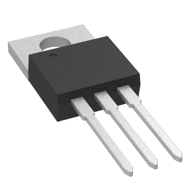
Figure 4. TO-220 Plastic Package
Top View
See Package Number NDE0003B
2
Submit Documentation Feedback
Copyright © 1999–2013, Texas Instruments Incorporated
Product Folder Links: LM195 LM395
�LM195, LM395
www.ti.com
SNOSBO4C – JUNE 1999 – REVISED APRIL 2013
These devices have limited built-in ESD protection. The leads should be shorted together or the device placed in conductive foam
during storage or handling to prevent electrostatic damage to the MOS gates.
ABSOLUTE MAXIMUM RATINGS (1) (2)
Collector to Emitter Voltage
LM195
42V
LM395
36V
Collector to Base Voltage
LM195
42V
LM395
36V
Base to Emitter Voltage (Forward)
LM195
LM395
42V
36V
Base to Emitter Voltage (Reverse)
20V
Collector Current
Internally Limited
Power Dissipation
Internally Limited
Operating Temperature Range
−55°C to +150°C
LM195
LM395
0°C to +125°C
−65°C to +150°C
Storage Temperature Range
Lead Temperature
(Soldering, 10 sec.)
(1)
260°C
“Absolute Maximum Ratings” indicate limits beyond which damage to the device may occur. Operating Ratings indicate conditions for
which the device is functional, but do not ensure specific performance limits.
If Military/Aerospace specified devices are required, please contact the Texas Instruments Sales Office/Distributors for availability and
specifications.
(2)
PRECONDITIONING
100% Burn-In In Thermal Limit
ELECTRICAL CHARACTERISTICS
Parameter
Conditions
LM195
Min
Collector-Emitter Operating Voltage
IQ ≤ IC ≤ IMAX
Base to Emitter Breakdown Voltage
0 ≤ VCE ≤ VCEMAX
42
TO-3, TO-220
VCE ≤ 15V
1.2
TO-5
VCE ≤ 7.0V
1.2
(2)
Typ
LM395
Max
Min
Typ
42
Max
Units
36
V
36
60
V
2.2
1.0
2.2
A
1.8
1.0
1.8
A
Collector Current
Saturation Voltage
IC ≤ 1.0A, TA = 25°C
Base Current
0 ≤ IC ≤ IMAX
0 ≤ VCE ≤ VCEMAX
Quiescent Current (IQ)
Vbe = 0
0 ≤ VCE ≤ VCEMAX
Base to Emitter Voltage
IC = 1.0A, TA = +25°C
Switching Time
VCE = 36V, RL = 36Ω,
TA = 25°C
(1)
(2)
1.8
2.0
1.8
2.2
V
3.0
5.0
3.0
10
μA
2.0
5.0
2.0
10
mA
0.9
0.9
V
500
500
ns
Unless otherwise specified, these specifications apply for −55°C ≤ Tj ≤ +150°C for the LM195 and 0°C ≤ +125°C for the LM395.
Selected devices with higher breakdown available.
Submit Documentation Feedback
Copyright © 1999–2013, Texas Instruments Incorporated
Product Folder Links: LM195 LM395
3
�LM195, LM395
SNOSBO4C – JUNE 1999 – REVISED APRIL 2013
www.ti.com
ELECTRICAL CHARACTERISTICS (continued)
(1)
Parameter
Thermal Resistance Junction to Case
Conditions
(3)
LM195
Min
Typ
Max
TO-3 Package (NDS)
2.3
TO-5 Package
12
TO-220 Package (NDE)
(3)
4
LM395
Min
Units
Typ
Max
3.0
2.3
3.0
°C/W
15
12
15
°C/W
4
6
°C/W
Without a heat sink, the thermal resistance of the TO-5 package is about +150°C/W, while that of the TO-3 package is +35°C/W.
Submit Documentation Feedback
Copyright © 1999–2013, Texas Instruments Incorporated
Product Folder Links: LM195 LM395
�LM195, LM395
www.ti.com
SNOSBO4C – JUNE 1999 – REVISED APRIL 2013
TYPICAL PERFORMANCE CHARACTERISTICS
(for NDS and NDE Packages)
Collector Characteristics
Short Circuit Current
Figure 5.
Figure 6.
Bias Current
Quiescent Current
Figure 7.
Figure 8.
Base Emitter Voltage
Base Current
Figure 9.
Figure 10.
Submit Documentation Feedback
Copyright © 1999–2013, Texas Instruments Incorporated
Product Folder Links: LM195 LM395
5
�LM195, LM395
SNOSBO4C – JUNE 1999 – REVISED APRIL 2013
www.ti.com
TYPICAL PERFORMANCE CHARACTERISTICS (continued)
(for NDS and NDE Packages)
6
Saturation Voltage
Response Time
Figure 11.
Figure 12.
Response Time
10V Transfer Function
Figure 13.
Figure 14.
36V Transfer Function
Transconductance
Figure 15.
Figure 16.
Submit Documentation Feedback
Copyright © 1999–2013, Texas Instruments Incorporated
Product Folder Links: LM195 LM395
�LM195, LM395
www.ti.com
SNOSBO4C – JUNE 1999 – REVISED APRIL 2013
TYPICAL PERFORMANCE CHARACTERISTICS (continued)
(for NDS and NDE Packages)
Small Signal Frequency
Response
Figure 17.
Submit Documentation Feedback
Copyright © 1999–2013, Texas Instruments Incorporated
Product Folder Links: LM195 LM395
7
�LM195, LM395
SNOSBO4C – JUNE 1999 – REVISED APRIL 2013
www.ti.com
SCHEMATIC DIAGRAM
8
Submit Documentation Feedback
Copyright © 1999–2013, Texas Instruments Incorporated
Product Folder Links: LM195 LM395
�LM195, LM395
www.ti.com
SNOSBO4C – JUNE 1999 – REVISED APRIL 2013
TYPICAL APPLICATIONS
*Solid Tantalum
Figure 18. 1.0 Amp Voltage Follower
*Protects against excessive base drive
**Needed for stability
Figure 19. Power PNP
Submit Documentation Feedback
Copyright © 1999–2013, Texas Instruments Incorporated
Product Folder Links: LM195 LM395
9
�LM195, LM395
SNOSBO4C – JUNE 1999 – REVISED APRIL 2013
www.ti.com
Figure 20. Time Delay
Figure 21. 1.0 MHz Oscillator
†Solid Tantalum
Figure 22. 1.0 Amp Negative Regulator
10
Submit Documentation Feedback
Copyright © 1999–2013, Texas Instruments Incorporated
Product Folder Links: LM195 LM395
�LM195, LM395
www.ti.com
SNOSBO4C – JUNE 1999 – REVISED APRIL 2013
†Solid Tantalum
Figure 23. 1.0 Amp Positive Voltage Regulator
Figure 24. Fast Optically Isolated Switch
Figure 25. Optically Isolated Power Transistor
Figure 26. CMOS or TTL Lamp Interface
Figure 27. Two Terminal Current Limiter
Submit Documentation Feedback
Copyright © 1999–2013, Texas Instruments Incorporated
Product Folder Links: LM195 LM395
11
�LM195, LM395
SNOSBO4C – JUNE 1999 – REVISED APRIL 2013
www.ti.com
*Drive Voltage 0V to ≥ 10V ≤ 42V
Figure 28. 40V Switch
Figure 29. 6.0V Shunt Regulator with Crowbar
Figure 30. Two Terminal 100 mA Current Regulator
12
Submit Documentation Feedback
Copyright © 1999–2013, Texas Instruments Incorporated
Product Folder Links: LM195 LM395
�LM195, LM395
www.ti.com
SNOSBO4C – JUNE 1999 – REVISED APRIL 2013
Turn ON = 350 mV
Turn OFF = 200 mV
Figure 31. Low Level Power Switch
T = R1C
R2 = 3R1
R2 ≤ 82k
Figure 32. Power One-Shot
*Need for Stability
Figure 33. Emitter Follower
Submit Documentation Feedback
Copyright © 1999–2013, Texas Instruments Incorporated
Product Folder Links: LM195 LM395
13
�LM195, LM395
SNOSBO4C – JUNE 1999 – REVISED APRIL 2013
www.ti.com
Figure 34. High Input Impedance AC Emitter Follower
*Prevents storage with fast fall time square wave drive
Figure 35. Fast Follower
14
Submit Documentation Feedback
Copyright © 1999–2013, Texas Instruments Incorporated
Product Folder Links: LM195 LM395
�LM195, LM395
www.ti.com
SNOSBO4C – JUNE 1999 – REVISED APRIL 2013
*Adjust for 50 mA quiescent current
†Solid Tantalum
Figure 36. Power Op Amp
*Sixty turns wound on Arnold Type A-083081-2 core.
**Four devices in parallel
†Solid tantalum
Figure 37. 6.0 Amp Variable Output Switching Regulator
Submit Documentation Feedback
Copyright © 1999–2013, Texas Instruments Incorporated
Product Folder Links: LM195 LM395
15
�LM195, LM395
SNOSBO4C – JUNE 1999 – REVISED APRIL 2013
www.ti.com
REVISION HISTORY
Changes from Revision B (April 2013) to Revision C
•
16
Page
Changed layout of National Data Sheet to TI format .......................................................................................................... 15
Submit Documentation Feedback
Copyright © 1999–2013, Texas Instruments Incorporated
Product Folder Links: LM195 LM395
�PACKAGE OPTION ADDENDUM
www.ti.com
30-Sep-2021
PACKAGING INFORMATION
Orderable Device
Status
(1)
Package Type Package Pins Package
Drawing
Qty
Eco Plan
(2)
Lead finish/
Ball material
MSL Peak Temp
Op Temp (°C)
Device Marking
(3)
(4/5)
(6)
LM395T
NRND
TO-220
NDE
3
45
Non-RoHS
& Green
Call TI
Level-1-NA-UNLIM
0 to 125
LM395T
LM395T/NOPB
ACTIVE
TO-220
NDE
3
45
RoHS & Green
SN
Level-1-NA-UNLIM
0 to 125
LM395T
(1)
The marketing status values are defined as follows:
ACTIVE: Product device recommended for new designs.
LIFEBUY: TI has announced that the device will be discontinued, and a lifetime-buy period is in effect.
NRND: Not recommended for new designs. Device is in production to support existing customers, but TI does not recommend using this part in a new design.
PREVIEW: Device has been announced but is not in production. Samples may or may not be available.
OBSOLETE: TI has discontinued the production of the device.
(2)
RoHS: TI defines "RoHS" to mean semiconductor products that are compliant with the current EU RoHS requirements for all 10 RoHS substances, including the requirement that RoHS substance
do not exceed 0.1% by weight in homogeneous materials. Where designed to be soldered at high temperatures, "RoHS" products are suitable for use in specified lead-free processes. TI may
reference these types of products as "Pb-Free".
RoHS Exempt: TI defines "RoHS Exempt" to mean products that contain lead but are compliant with EU RoHS pursuant to a specific EU RoHS exemption.
Green: TI defines "Green" to mean the content of Chlorine (Cl) and Bromine (Br) based flame retardants meet JS709B low halogen requirements of