LM4125
www.ti.com
SNVS238A – MAY 2004 – REVISED APRIL 2013
LM4125 Precision Micropower Low Dropout Voltage Reference
Check for Samples: LM4125
FEATURES
DESCRIPTION
•
•
•
•
•
•
•
•
•
The LM4125 is a precision low power low dropout
bandgap voltage reference with up to 5 mA output
current source and sink capability.
1
2
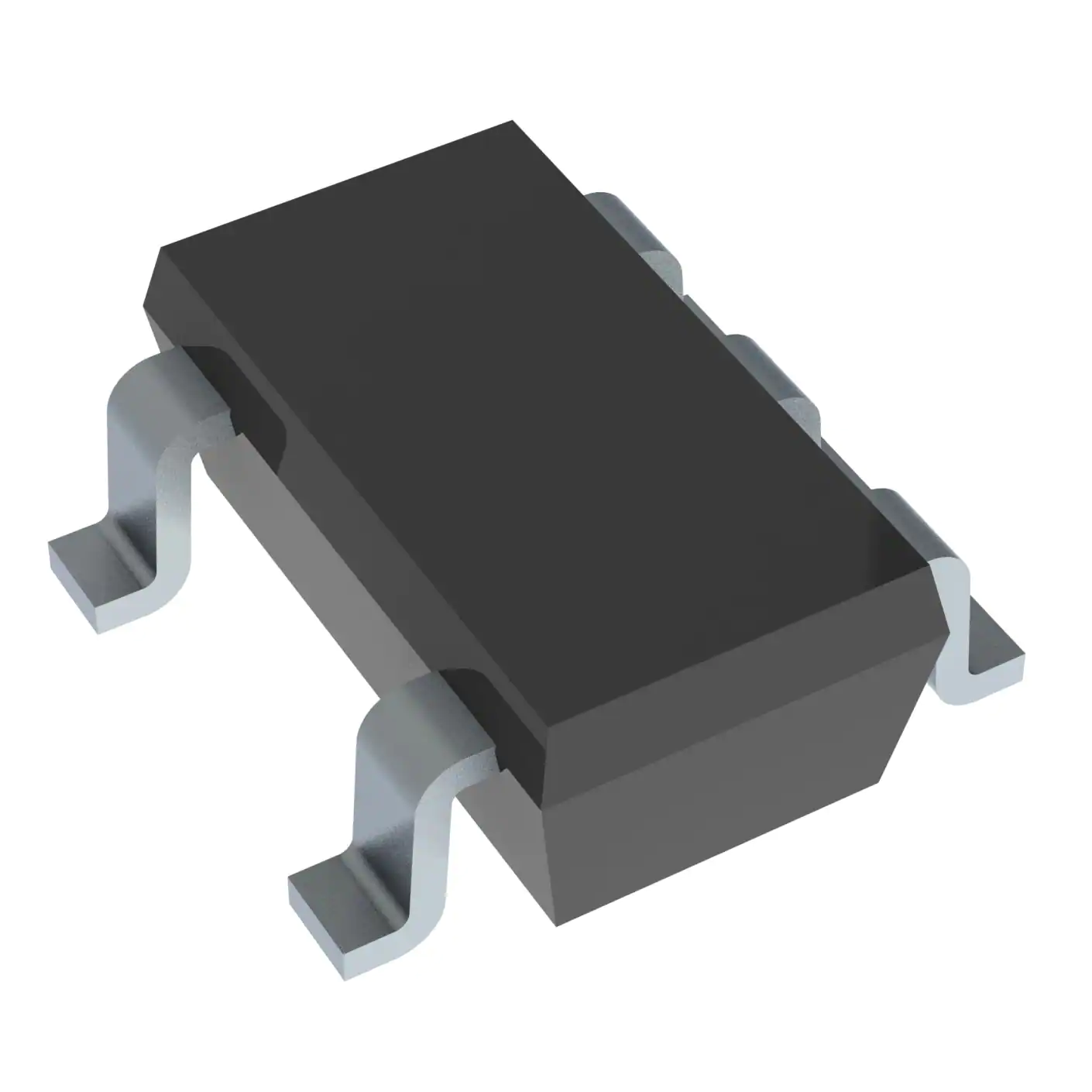
Small SOT23-5 Package
Low Dropout Voltage: 120 mV Typ @ 1 mA
High Output Voltage Accuracy: 0.2%
Source and Sink Current Output: ±5 mA
Supply Current: 160 μA Typ.
Low Temperature Coefficient: 50 ppm/°C
Fixed Output Voltages: 2.048, 2.5,and 4.096
Industrial Temperature Range: −40°C to +85°C
(For Extended Temperature Range, −40°C to
125°C, Contact TI)
APPLICATIONS
•
•
•
•
•
•
•
•
•
•
Portable, Battery Powered Equipment
Instrumentation and Process Control
Automotive & Industrial
Test Equipment
Data Acquisition Systems
Precision Regulators
Battery Chargers
Base Stations
Communications
Medical Equipment
This series reference operates with input voltages as
low as 2V and up to 6V consuming 160 µA (Typ.)
supply current. In power down mode, device current
drops to less than 2 μA.
The LM4125 comes in two grades (A and Standard)
and three voltage options for greater flexibility. The
best grade devices (A) have an initial accuracy of
0.2%, while the standard have an initial accuracy of
0.5%, both with a tempco of 50ppm/°C ensured from
−40°C to +125°C.
The very low dropout voltage, low supply current and
power-down capability of the LM4125 makes this
product an ideal choice for battery powered and
portable applications.
The device performance is ensured over the industrial
temperature range (−40°C to +85°C), while certain
specs are ensured over the extended temperature
range (−40°C to +125°C). Please contact TI for full
specifications over the extended temperature range.
The LM4125 is available in a standard 5-pin SOT-23
package.
Connection Diagram
Figure 1. 5-Pin SOT-23 Surface Mount Package
See Package Number DBV
These devices have limited built-in ESD protection. The leads should be shorted together or the device placed in conductive foam
during storage or handling to prevent electrostatic damage to the MOS gates.
1
2
Please be aware that an important notice concerning availability, standard warranty, and use in critical applications of
Texas Instruments semiconductor products and disclaimers thereto appears at the end of this data sheet.
All trademarks are the property of their respective owners.
PRODUCTION DATA information is current as of publication date.
Products conform to specifications per the terms of the Texas
Instruments standard warranty. Production processing does not
necessarily include testing of all parameters.
Copyright © 2004–2013, Texas Instruments Incorporated
�LM4125
SNVS238A – MAY 2004 – REVISED APRIL 2013
www.ti.com
Absolute Maximum Ratings (1) (2)
−0.3V to 8V
Maximum Voltage on input or enable pins
Output Short-Circuit Duration
Power Dissipation (TA = 25°C) (3)
ESD Susceptibility
(4)
Indefinite
DBV package − θJA
280°C/W
Power Dissipation
350 mW
Human Body Model
Machine Model
Lead Temperature:
(1)
(2)
(3)
(4)
2 kV
200V
Soldering, (10 sec.)
+260°C
Vapor Phase (60 sec.)
+215°C
Infrared (15 sec.)
+220°C
“Absolute Maximum Ratings” indicate limits beyond which damage to the device may occur. Operating Ratings indicate conditions for
which the device is intended to be functional, but do not ensure specific performance limits. For ensured specifications and test
conditions, see Electrical Characteristics. The ensured specifications apply only for the test conditions listed. Some performance
characteristics may degrade when the device is not operated under the listed test conditions.
If Military/Aerospace specified devices are required, please contact the Texas Instruments Sales Office/Distributors for availability and
specifications.
Without PCB copper enhancements. The maximum power dissipation must be de-rated at elevated temperatures and is limited by TJMAX
(maximum junction temperature), θJ-A (junction to ambient thermal resistance) and TA (ambient temperature). The maximum power
dissipation at any temperature is: PDissMAX = (TJMAX − TA)/θJ-A up to the value listed in the Absolute Maximum Ratings.
The human body model is a 100 pF capacitor discharged through a 1.5 kΩ resistor into each pin. The machine model is a 200 pF
capacitor discharged directly into each pin.
Operating Range (1)
−65°C to +150°C
Storage Temperature Range
Ambient Temperature Range
−40°C to +85°C
Junction Temperature Range
−40°C to +125°C
(1)
2
“Absolute Maximum Ratings” indicate limits beyond which damage to the device may occur. Operating Ratings indicate conditions for
which the device is intended to be functional, but do not ensure specific performance limits. For ensured specifications and test
conditions, see Electrical Characteristics. The ensured specifications apply only for the test conditions listed. Some performance
characteristics may degrade when the device is not operated under the listed test conditions.
Submit Documentation Feedback
Copyright © 2004–2013, Texas Instruments Incorporated
Product Folder Links: LM4125
�LM4125
www.ti.com
SNVS238A – MAY 2004 – REVISED APRIL 2013
Electrical Characteristics — LM4125-2.048V and 2.5V
Unless otherwise specified VIN = 3.3V, ILOAD = 0, COUT = 0.01µF, TA = Tj = 25°C. Limits with standard typeface are for Tj =
25°C, and limits in boldface type apply over the −40°C ≤ TA ≤ +85°C temperature range.
Symbol
VOUT
Parameter
Conditions
Output Voltage Initial Accuracy
LM4125A-2.048
LM4125A-2.500
±0.2
%
LM4125-2.048
LM4125-2.500
±0.5
%
Temperature Coefficient
−40°C ≤ TA ≤ +125°C
Line Regulation
3.3V ≤ VIN ≤ 6V
Load Regulation
Dropout Voltage (3)
Output Noise Voltage (4)
VN
IS
(1)
(2)
14
50
ppm/°c
0.0007
0.008
0.01
%/V
0 mA ≤ ILOAD ≤ 1 mA
0.03
0.08
0.17
1 mA ≤ ILOAD ≤ 5 mA
0.01
0.04
0.1
−1 mA ≤ ILOAD ≤ 0 mA
0.04
0.12
−5 mA ≤ ILOAD ≤ −1 mA
0.01
45
65
100
ILOAD = +1 mA
120
150
200
ILOAD = +5 mA
180
210
300
0.1 Hz to 10 Hz
20
µVPP
10 Hz to 10 kHz
36
µVPP
160
VIN = 3.3V, VOUT = 0
ISC
Short Circuit Current
Hyst
Thermal Hysteresis (5)
(1)
(2)
(3)
(4)
(5)
(6)
Long Term Stability
mV
257
290
µA
15
6
VIN = 6V, VOUT = 0
30
mA
17
6
(6)
%/mA
ILOAD = 0 mA
Supply Current
ΔVOUT
Max
Units
ΔVOUT/ΔVIN
VIN−VOUT
Typ
(1)
TCVOUT/°C
ΔVOUT/ΔILOAD
Min
30
−40°C ≤ TA ≤ 125°C
0.5
mV/V
1000 hrs. @ 25°C
100
ppm
Limits are 100% production tested at 25°C. Limits over the operating temperature range are ensured through correlation using Statistical
Quality Control (SQC) methods. The limits are used to calculate Outgoing Quality Level (AOQL).
Typical numbers are at 25°C and represent the most likely parametric norm.
Dropout voltage is the differential voltage between VOUT and VIN at which VOUT changes ≤ 1% from VOUT at VIN = 3.3V for 2.0V, 2.5V
and 5V for 4.1V. A parasitic diode exists between input and output pins; it will conduct if VOUT is pulled to a higher voltage than VIN.
Output noise voltage is proportional to VOUT. VN for other voltage option is calculated using (VN(1.8V)/1.8) * VOUT. VN (2.5V) =
(36µVPP/1.8) * 2.5 = 46µVPP.
Thermal hysteresis is defined as the change in +25°C output voltage before and after exposing the device to temperature extremes.
Long term stability is change in VREF at 25°C measured continuously during 1000 hrs.
Submit Documentation Feedback
Copyright © 2004–2013, Texas Instruments Incorporated
Product Folder Links: LM4125
3
�LM4125
SNVS238A – MAY 2004 – REVISED APRIL 2013
www.ti.com
Electrical Characteristics — LM4125-4.096V
Unless otherwise specified VIN = 5V, ILOAD = 0, COUT = 0.01µF, TA = Tj = 25°C. Limits with standard typeface are for Tj = 25°C,
and limits in boldface type apply over the −40°C ≤ TA ≤ +85°C temperature range.
Symbol
VOUT
Parameter
Conditions
Output Voltage Initial
Accuracy
LM4125A-4.096
±0.2
%
LM4125-4.096
±0.5
%
Temperature Coefficient
−40°C ≤ TA ≤ +125°C
Line Regulation
5V ≤ VIN ≤ 6V
Load Regulation
Dropout Voltage (3)
Output Noise Voltage (4)
VN
IS
Max
Units
ΔVOUT/ΔVIN
VIN−VOUT
Typ
(1)
TCVOUT/°C
ΔVOUT/ΔILOAD
Min
(1)
(2)
14
50
ppm/°c
0.0007
0.008
0.01
%/V
0 mA ≤ ILOAD ≤ 1 mA
0.03
0.08
0.17
1 mA ≤ ILOAD ≤ 5 mA
0.01
0.04
0.1
−1 mA ≤ ILOAD ≤ 0 mA
0.04
0.12
−5 mA ≤ ILOAD ≤ −1 mA
0.01
ILOAD = 0 mA
45
65
100
ILOAD = +1 mA
120
150
200
ILOAD = +5 mA
180
210
300
0.1 Hz to 10 Hz
20
10 Hz to 10 kHz
36
Supply Current
160
VOUT = 0
%/mA
mV
µVPP
µVPP
257
290
µA
15
6
30
ISC
Short Circuit Current
Hyst
Thermal Hysteresis (5)
−40°C ≤ TA ≤ 125°C
0.5
mV/V
ΔVOUT
Long Term Stability (6)
1000 hrs. @ 25°C
100
ppm
VIN = 6V, VOUT = 0
17
6
(1)
(2)
(3)
(4)
(5)
(6)
4
mA
30
Limits are 100% production tested at 25°C. Limits over the operating temperature range are ensured through correlation using Statistical
Quality Control (SQC) methods. The limits are used to calculate Outgoing Quality Level (AOQL).
Typical numbers are at 25°C and represent the most likely parametric norm.
Dropout voltage is the differential voltage between VOUT and VIN at which VOUT changes ≤ 1% from VOUT at VIN = 3.3V for 2.0V, 2.5V
and 5V for 4.1V. A parasitic diode exists between input and output pins; it will conduct if VOUT is pulled to a higher voltage than VIN.
Output noise voltage is proportional to VOUT. VN for other voltage option is calculated using (VN(1.8V)/1.8) * VOUT. VN (2.5V) =
(36µVPP/1.8) * 2.5 = 46µVPP.
Thermal hysteresis is defined as the change in +25°C output voltage before and after exposing the device to temperature extremes.
Long term stability is change in VREF at 25°C measured continuously during 1000 hrs.
Submit Documentation Feedback
Copyright © 2004–2013, Texas Instruments Incorporated
Product Folder Links: LM4125
�LM4125
www.ti.com
SNVS238A – MAY 2004 – REVISED APRIL 2013
LM4125 Typical Operating Characteristics
Unless otherwise specified, VIN = 3.3V, VOUT = 2.5V, ILOAD = 0, COUT = 0.022µF and TA = 25°C.
Long Term Drift
Typical Temperature Drift
Figure 2.
Figure 3.
Short Circuit Current
vs
Temperature
Dropout Voltage
vs
Output Error
Figure 4.
Figure 5.
Dropout Voltage
vs
Load Current
Load Regulation
Figure 6.
Figure 7.
Submit Documentation Feedback
Copyright © 2004–2013, Texas Instruments Incorporated
Product Folder Links: LM4125
5
�LM4125
SNVS238A – MAY 2004 – REVISED APRIL 2013
www.ti.com
LM4125 Typical Operating Characteristics (continued)
Unless otherwise specified, VIN = 3.3V, VOUT = 2.5V, ILOAD = 0, COUT = 0.022µF and TA = 25°C.
6
GND Pin Current
GND Pin Current at No Load
vs
Temperature
Figure 8.
Figure 9.
GND Pin Current
vs
Load
0.1Hz to 10Hz output Noise
Figure 10.
Figure 11.
Output Impedance
vs
Frequency
PSRR
vs
Frequency
Figure 12.
Figure 13.
Submit Documentation Feedback
Copyright © 2004–2013, Texas Instruments Incorporated
Product Folder Links: LM4125
�LM4125
www.ti.com
SNVS238A – MAY 2004 – REVISED APRIL 2013
LM4125 Typical Operating Characteristics (continued)
Unless otherwise specified, VIN = 3.3V, VOUT = 2.5V, ILOAD = 0, COUT = 0.022µF and TA = 25°C.
Start-Up Response
Load Step Response
Figure 14.
Figure 15.
Load Step Response
Line Step Response
Figure 16.
Figure 17.
Thermal Hysteresis
Figure 18.
Submit Documentation Feedback
Copyright © 2004–2013, Texas Instruments Incorporated
Product Folder Links: LM4125
7
�LM4125
SNVS238A – MAY 2004 – REVISED APRIL 2013
www.ti.com
PIN FUNCTIONS
Output (Pin 5): Reference Output.
Input (Pin 4): Positive Supply.
Ground (Pin 2): Negative Supply or Ground Connection.
APPLICATION HINTS
The standard application circuit for the LM4125 is shown in Figure 19. It is designed to be stable with ceramic
output capacitors in the range of 0.022µF to 0.1µF. Note that 0.022µF is the minimum required output capacitor.
These capacitors typically have an ESR of about 0.1 to 0.5Ω. Smaller ESR can be tolerated, however larger ESR
can not. The output capacitor can be increased to improve load transient response, up to about 1µF. However,
values above 0.047µF must be tantalum. With tantalum capacitors, in the 1µF range, a small capacitor between
the output and the reference pin is required. This capacitor will typically be in the 50pF range. Care must be
taken when using output capacitors of 1µF or larger. These application must be thoroughly tested over
temperature, line and load.
An input capacitor is typically not required. However, a 0.1µF ceramic can be used to help prevent line transients
from entering the LM4125. Larger input capacitors should be tantalum or aluminum.
The typical thermal hysteresis specification is defined as the change in +25°C voltage measured after thermal
cycling. The device is thermal cycled to temperature -40°C and then measured at 25°C. Next the device is
thermal cycled to temperature +125°C and again measured at 25°C. The resulting VOUT delta shift between the
25°C measurements is thermal hysteresis. Thermal hysteresis is common in precision references and is induced
by thermal-mechanical package stress. Changes in environmental storage temperature, operating temperature
and board mounting temperature are all factors that can contribute to thermal hysteresis.
Figure 19. Standard Application Circuit
INPUT CAPACITOR
Noise on the power-supply input can effect the output noise, but can be reduced by using an optional bypass
capacitor between the input pin and the ground.
PRINTED CIRCUIT BOARD LAYOUT CONSIDERATION
The mechanical stress due to PC board mounting can cause the output voltage to shift from its initial value.
References in SOT packages are generally less prone to assembly stress than devices in Small Outline (SOIC)
package.
To reduce the stress-related output voltage shifts, mount the reference on the low flex areas of the PC board
such as near to the edge or the corner of the PC board.
8
Submit Documentation Feedback
Copyright © 2004–2013, Texas Instruments Incorporated
Product Folder Links: LM4125
�LM4125
www.ti.com
SNVS238A – MAY 2004 – REVISED APRIL 2013
Typical Application Circuits
Figure 20. Voltage Reference with Negative Output
Figure 21. Precision High Current Low Dropout
Regulator
Figure 22. Precision High Current Negative Voltage
Regulator
Figure 23. Voltage Reference with Complimentary
Output
Figure 24. Precision High Current Low Droput
Regulator
Figure 25. Precision Voltage Reference with Force
and Sense Output
Submit Documentation Feedback
Copyright © 2004–2013, Texas Instruments Incorporated
Product Folder Links: LM4125
9
�LM4125
SNVS238A – MAY 2004 – REVISED APRIL 2013
www.ti.com
Figure 26. Programmable Current Source
Figure 27. Precision Regulator with Current
Limiting Circuit
Figure 28. Power Supply Splitter
10
Submit Documentation Feedback
Copyright © 2004–2013, Texas Instruments Incorporated
Product Folder Links: LM4125
�LM4125
www.ti.com
SNVS238A – MAY 2004 – REVISED APRIL 2013
REVISION HISTORY
Changes from Original (April 2013) to Revision A
•
Page
Changed layout of National Data Sheet to TI format .......................................................................................................... 10
Submit Documentation Feedback
Copyright © 2004–2013, Texas Instruments Incorporated
Product Folder Links: LM4125
11
�PACKAGE OPTION ADDENDUM
www.ti.com
10-Dec-2020
PACKAGING INFORMATION
Orderable Device
Status
(1)
Package Type Package Pins Package
Drawing
Qty
Eco Plan
(2)
Lead finish/
Ball material
MSL Peak Temp
Op Temp (°C)
Device Marking
(3)
(4/5)
(6)
LM4125AIM5-2.5/NOPB
ACTIVE
SOT-23
DBV
5
1000
RoHS & Green
SN
Level-1-260C-UNLIM
-40 to 125
R81A
LM4125IM5-2.0/NOPB
ACTIVE
SOT-23
DBV
5
1000
RoHS & Green
SN
Level-1-260C-UNLIM
-40 to 125
R80B
LM4125IM5-2.5/NOPB
ACTIVE
SOT-23
DBV
5
1000
RoHS & Green
SN
Level-1-260C-UNLIM
-40 to 125
R81B
(1)
The marketing status values are defined as follows:
ACTIVE: Product device recommended for new designs.
LIFEBUY: TI has announced that the device will be discontinued, and a lifetime-buy period is in effect.
NRND: Not recommended for new designs. Device is in production to support existing customers, but TI does not recommend using this part in a new design.
PREVIEW: Device has been announced but is not in production. Samples may or may not be available.
OBSOLETE: TI has discontinued the production of the device.
(2)
RoHS: TI defines "RoHS" to mean semiconductor products that are compliant with the current EU RoHS requirements for all 10 RoHS substances, including the requirement that RoHS substance
do not exceed 0.1% by weight in homogeneous materials. Where designed to be soldered at high temperatures, "RoHS" products are suitable for use in specified lead-free processes. TI may
reference these types of products as "Pb-Free".
RoHS Exempt: TI defines "RoHS Exempt" to mean products that contain lead but are compliant with EU RoHS pursuant to a specific EU RoHS exemption.
Green: TI defines "Green" to mean the content of Chlorine (Cl) and Bromine (Br) based flame retardants meet JS709B low halogen requirements of


 工商网监
湘ICP备2023018690号
工商网监
湘ICP备2023018690号
