OBSOLETE
LM4130
www.ti.com
SNVS048D – NOVEMBER 1999 – REVISED APRIL 2013
LM4130 Precision Micropower Low Dropout Voltage Reference
Check for Samples: LM4130
FEATURES
DESCRIPTION
•
•
•
•
•
•
•
•
•
•
•
•
The LM4130 family of precision voltage references
performs comparable to the best laser-trimmed
bipolar references, but in cost effective CMOS
technology. Key to this break through is the use of
EEPROM registers for correction of curvature,
tempco, and accuracy on a CMOS bandgap
architecture that allows package level programming
to overcome assembly shift. The shifts in voltage
accuracy and tempco during assembly of die into
plastic packages limit the accuracy of references
trimmed with laser techniques.
1
2
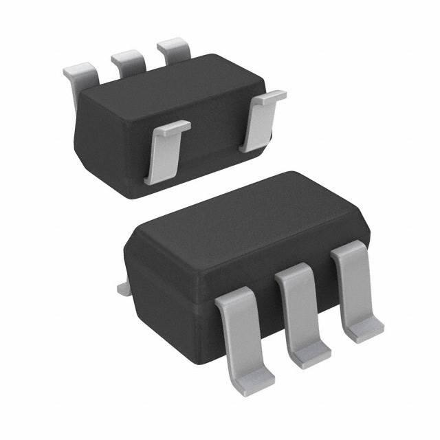
Small SOT23-5 package
High output voltage accuracy 0.05%
Low Temperature Coefficient 10 ppm/°C
Stable with capacitive loads to 100µF
Low dropout voltage ≤275 mV @ 10 mA
Supply Current ≤75 μA
Full accuracy −40°C to 85°C
Extended operation to 125°C
Excellent load and line regulation
Output current 20 mA
Output impedance < 1Ω
Voltage options: 2.500V and 4.096V
APPLICATIONS SUMMARY
•
•
•
•
•
•
•
•
•
•
•
Portable, battery powered equipment
Instrumentation and process control
Automotive & Industrial
Test equipment
Data acquisition systems
Precision regulators
Battery chargers
Base stations
Communications
Medical equipment
Servo systems
Unlike other LDO references, the LM4130 requires no
output capacitor. Neither is a buffer amplifier required,
even with loads up to 20mA. These advantages and
the SOT23 packaging are important for cost-critical
and space-critical applications.
Series references provide lower power consumption
than shunt references, since they don't have to idle
the maximum possible load current under no load
conditions. This advantage, the low quiescent current
(75µA), and the low dropout voltage(275mV) make
the LM4130 ideal for battery-powered solutions.
The LM4130 is available in five grades (A, B, C, D
and E) for greater flexibility. The best grade devices
(A) have an initial accuracy of 0.05% with ensured
temperature coefficient of 10ppm/°C or less, while the
lowest grade parts (E) have an initial accuracy of
0.5% and a tempco of 30ppm/°C.
Connection Diagram and Pin Configuration
*Optional, Recommended for improved transient response and
input noise reduction.
(See Application Information)
1
2
Please be aware that an important notice concerning availability, standard warranty, and use in critical applications of
Texas Instruments semiconductor products and disclaimers thereto appears at the end of this data sheet.
All trademarks are the property of their respective owners.
PRODUCTION DATA information is current as of publication date.
Products conform to specifications per the terms of the Texas
Instruments standard warranty. Production processing does not
necessarily include testing of all parameters.
Copyright © 1999–2013, Texas Instruments Incorporated
�OBSOLETE
LM4130
SNVS048D – NOVEMBER 1999 – REVISED APRIL 2013
www.ti.com
Refer to the Ordering Information Table in this Data Sheet for Specific Part Number
Figure 1. SOT23-5 Surface Mount Package
Table 1. SOT23-5 Package Marking InformationOnly four fields of marking are possible on the SOT23-5's
small surface. This table gives the meaning of the four fields.
Field Information
First Field:
R = Reference
Second and Third Field:
03 = 2.50V Voltage Option
04 = 4.096V Voltage Option
Fourth Field:
A-E = Initial Reference Voltage Tolerance and Temperature Coefficient
A = ±0.05%, 10ppm/°C
B = ±0.2%, 10ppm/°C
C = ±0.1%, 20ppm/°C
D = ±0.4%, 20ppm/°C
E = ±0.5%, 30ppm/°C
These devices have limited built-in ESD protection. The leads should be shorted together or the device placed in conductive foam
during storage or handling to prevent electrostatic damage to the MOS gates.
Absolute Maximum Ratings
(1)
−0.3V to 6V
Maximum Voltage on any Input
Output Short-Circuit Duration
Indefinite
Power Dissipation (TA = 25°C)
350 mW
(2)
ESD Susceptibility
(3)
Human Body Model
2 kV
Machine Model
200V
Lead Temperature:
(1)
(2)
(3)
2
Soldering, (10 sec.)
+260°C
Vapor Phase (60 sec.)
+215°C
Infrared (15 sec.)
+220°C
Absolute Maximum Ratings indicate limits beyond which damage to the device may occur. Operating Ratings indicate conditions for
which the device is intended to be functional, but do not ensure specific performance limits. For ensured specifications and test
conditions, see Electrical Characteristics. The ensured specifications apply only for the test conditions listed. Some performance
characteristics may degrade when the device is not operated under the listed test conditions.
Without PCB copper enhancements. The maximum power dissipation must be de-rated at elevated temperatures and is limited by TJMAX
(maximum junction temperature), θJ-A (junction to ambient thermal resistance) and TA (ambient temperature). The maximum power
dissipation at any temperature is: PDissMAX = (TJMAX − TA)/θJ-A up to the value listed in the Absolute Maximum Ratings. θJ-A for SOT235 package is 220°C/W, TJMAX = 125°C.
The human body model is a 100 pF capacitor discharged through a 1.5 kΩ resistor into each pin. The machine model is a 200 pF
capacitor discharged directly into each pin.
Submit Documentation Feedback
Copyright © 1999–2013, Texas Instruments Incorporated
Product Folder Links: LM4130
�OBSOLETE
LM4130
www.ti.com
Operating Range
SNVS048D – NOVEMBER 1999 – REVISED APRIL 2013
(1)
−65°C to +150°C
Storage Temperature Range
−40°C to +85°C
Operating Temperature Range
(1)
Absolute Maximum Ratings indicate limits beyond which damage to the device may occur. Operating Ratings indicate conditions for
which the device is intended to be functional, but do not ensure specific performance limits. For ensured specifications and test
conditions, see Electrical Characteristics. The ensured specifications apply only for the test conditions listed. Some performance
characteristics may degrade when the device is not operated under the listed test conditions.
Submit Documentation Feedback
Copyright © 1999–2013, Texas Instruments Incorporated
Product Folder Links: LM4130
3
�OBSOLETE
LM4130
SNVS048D – NOVEMBER 1999 – REVISED APRIL 2013
www.ti.com
LM4130-2.500
Electrical Characteristics
Unless otherwise specified VCC = 5V, ILOAD = 0 TA = 25°C. Limits with standard typeface are for TA = 25°C, and limits in
boldface type apply over the operating temperature range.
Symbol
VREF
Parameter
Conditions
Min
(1)
Typ
(2)
Output Voltage Initial
Accuracy
LM4130A-2.500
LM4130B-2.500
LM4130C-2.500
LM4130D-2.500
LM4130E-2.500
TCVREF/°C
(3)
±0.05
±0.2
±0.1
±0.4
±0.5
ppm/°C
0°C ≤ TA ≤ +85°C
−40°C ≤ TA ≤ +85°C
10
20
LM4130C, D
20
LM4130E
30
Line Regulation
ILOAD = 100µA
ppm/V
30
VREF + 400 mV ≤ VIN ≤ 5.5V
Load Regulation
Long-Term Stability
(4)
25
1000 Hrs
50
−40°C ≤ TA ≤ +125°C
50
VIN - VREF
Dropout Voltage
ILOAD = 10 mA
VN
Output Noise Voltage
0.1 Hz to 10 Hz
IS
Supply Current
ISC
Short Circuit Current
(5)
(1)
(2)
(3)
(4)
(5)
(6)
4
(6)
100
150
0 mA ≤ ILOAD ≤ 20 mA
Thermal Hysteresis
ΔVREF
Units
%
VREF + 200 mV ≤ VIN ≤ 5.5V
ΔVREF/ΔILOAD
(1)
Temperature Coefficient
LM4130A, B
ΔVREF/ΔVIN
Max
60
80
ppm
275
400
30
mV
μVPP
150
50
ppm/mA
75
90
μA
60
mA
65
mA
Limits are 100% production tested at 25°C. Limits over the operating temperature range are ensured through correlation using Statistical
Quality Control (SQC) methods. The limits are used to calculate TI's Average Outgoing Quality Level (AOQL).
Typical numbers are at 25°C and represent the most likely parametric norm.
Temperature coefficient is measured by the "Box" method; i.e., the maximum ΔVREF is divided by the maximum ΔT.
Long term stability is VREF @25°C measured during 1000 hrs.
Thermal hysteresis is defined as the change in +25°C output voltage before and after cycling the device from −40°C to 125°C.
Dropout voltage is defined as the minimum input to output differential at which the output voltage drops by 0.5% below the value
measured with a 5V input.
Submit Documentation Feedback
Copyright © 1999–2013, Texas Instruments Incorporated
Product Folder Links: LM4130
�OBSOLETE
LM4130
www.ti.com
SNVS048D – NOVEMBER 1999 – REVISED APRIL 2013
LM4130-4.096
Electrical Characteristics
Unless otherwise specified VCC = 5.0V, ILOAD = 0 TA = 25°C. Limits with standard typeface are for TA = 25°C, and limits in
boldface type apply over the operating temperature range.
Symbol
VREF
TCVREF/°C
(3)
Parameter
Conditions
ΔVREF/ΔILOAD
(1)
Typ
(2)
Output Voltage Initial
Accuracy
LM4130-4.096A
LM4130-4.096B
LM4130-4.096C
LM4130-4.096D
LM4130-4.096E
±0.05
±0.2
±0.1
±0.4
±0.5
ppm/°C
0°C ≤ TA ≤ +85°C
−40°C ≤ TA ≤ +85°C
10
20
20
LM4130E
30
Line Regulation
ILOAD = 100µA
Load Regulation
(4)
VREF + 500 mV ≤ VIN ≤ 5.5V
75
250
400
ppm/V
0 mA ≤ ILOAD ≤ 20 mA
16
60
80
ppm/mA
1000 Hrs
50
−40°C ≤ TA ≤ +125°C
50
VIN - VREF
Dropout Voltage
ILOAD = 10 mA
VN
Output Noise Voltage
0.1 Hz to 10 Hz
IS
Supply Current
ISC
Short Circuit Current
(5)
(2)
(3)
(4)
(5)
(6)
Units
%
Thermal Hysteresis
(1)
(1)
LM4130C, D
Long-Term Stability
ΔVREF
Max
Temperature Coefficient
LM4130A, B
ΔVREF/ΔVIN
Min
(6)
ppm
275
500
μVPP
245
50
30
mV
75
90
μA
60
mA
65
mA
Limits are 100% production tested at 25°C. Limits over the operating temperature range are ensured through correlation using Statistical
Quality Control (SQC) methods. The limits are used to calculate TI's Average Outgoing Quality Level (AOQL).
Typical numbers are at 25°C and represent the most likely parametric norm.
Temperature coefficient is measured by the "Box" method; i.e., the maximum ΔVREF is divided by the maximum ΔT.
Long term stability is VREF @25°C measured during 1000 hrs.
Thermal hysteresis is defined as the change in +25°C output voltage before and after cycling the device from −40°C to 125°C.
Dropout voltage is defined as the minimum input to output differential at which the output voltage drops by 0.5% below the value
measured with a 5V input.
Submit Documentation Feedback
Copyright © 1999–2013, Texas Instruments Incorporated
Product Folder Links: LM4130
5
�OBSOLETE
LM4130
SNVS048D – NOVEMBER 1999 – REVISED APRIL 2013
www.ti.com
LM4130 Typical Performance Characteristics
TA = 25°C, No Load, VIN = 5.0V, unless otherwise noted.
6
Temperature Drift Characteristics
Load Regulation
vs
Temperature
Line Regulation
vs
Load
Line Regulation
vs
Temperature
Output Voltage
vs
Load Current
Dropout
vs
Load (VREF = 2.5)
Submit Documentation Feedback
Copyright © 1999–2013, Texas Instruments Incorporated
Product Folder Links: LM4130
�OBSOLETE
LM4130
www.ti.com
SNVS048D – NOVEMBER 1999 – REVISED APRIL 2013
LM4130 Typical Performance Characteristics (continued)
TA = 25°C, No Load, VIN = 5.0V, unless otherwise noted.
Supply Current
vs
Temperature
Short Circuit Current
vs
Temperature
Power-Up Response (4.096V)
Output Impedance
Power Supply Rejection Ratio
Load Transient Response
Submit Documentation Feedback
Copyright © 1999–2013, Texas Instruments Incorporated
Product Folder Links: LM4130
7
�OBSOLETE
LM4130
SNVS048D – NOVEMBER 1999 – REVISED APRIL 2013
www.ti.com
LM4130 Typical Performance Characteristics (continued)
TA = 25°C, No Load, VIN = 5.0V, unless otherwise noted.
Line Transient Response
0.1Hz to 10 Hz Noise (VREF = 2.5V)
Output Noise Spectra
Pin Functions
VREF (Pin 5): Reference Output. The output of the LM4130 can source up to 20 mA. It is stable with output
capacitor ranges from 0 to 100 µF.
VIN (Pin 4): Positive Supply. Bypassing with a 0.1µF capacitor is recommended if the output loading changes or
input is noisy.
Ground (Pin 2): Negative Supply or Ground Connection.
NC (Pins 1, 3): No Connection (internally terminated). These pins must be left unconnected.
Application Information
OUTPUT CAPACITOR
The LM4130 is designed to operate with or without an output capacitor and is stable with capacitive loads of up
to 100 µF.
Connecting a capacitor between the output and ground will significantly improve the load transient response
when switching from a light load to a heavy load. However, the output capacitor should not be made arbitrarily
large because it will effect the turn-on time as well as line and load transients.
INPUT CAPACITOR
A small 0.1µF capacitor on the input significantly improves stability under a wide range of load conditions. With
an input bypass capacitor, the LM4130 will drive any combination of resistance and capacitance up to
VREF/20mA and 100 µF respectively.
Noise on the power-supply input can effect the output noise, but it can be reduced by using an optional bypass
capacitor between the input pin and the ground.
8
Submit Documentation Feedback
Copyright © 1999–2013, Texas Instruments Incorporated
Product Folder Links: LM4130
�OBSOLETE
LM4130
www.ti.com
SNVS048D – NOVEMBER 1999 – REVISED APRIL 2013
PRINTED CIRCUIT BOARD LAYOUT CONSIDERATION
References in SOT packages are generally less prone to assembly stress than devices in Small Outline (SOIC)
package.
To minimize the mechanical stress due to PC board mounting that can cause the output voltage to shift from its
initial value, mount the reference on a low flex area of the PC board, such as near the edge or a corner.
Typical Application Circuits
Figure 2. Precision High Current Low Dropout Regulator
Figure 3. Voltage Reference with Complimentary Output
Figure 4. Precision High Current Low Dropout Regulator
Figure 5. Precision Voltage Reference with Force and Sense Output
Submit Documentation Feedback
Copyright © 1999–2013, Texas Instruments Incorporated
Product Folder Links: LM4130
9
�OBSOLETE
LM4130
SNVS048D – NOVEMBER 1999 – REVISED APRIL 2013
www.ti.com
Figure 6. Programmable Current Source
Figure 7. Precision Regulator with Current Limiting Circuit
Figure 8. Low Cost Higher Output Current Circuit
* Select R1 to deliver 80% of typical load current. The LM4130 then will source as necessary, up to 20mA, to maintain
the output regulation. Care must be taken not to remove the load as the output will be driven to the rail. This
approach will effect line regulation.
Figure 9. Supply Splitter
10
Submit Documentation Feedback
Copyright © 1999–2013, Texas Instruments Incorporated
Product Folder Links: LM4130
�OBSOLETE
LM4130
www.ti.com
SNVS048D – NOVEMBER 1999 – REVISED APRIL 2013
REVISION HISTORY
Changes from Revision C (April 2013) to Revision D
•
Page
Changed layout of National Data Sheet to TI format .......................................................................................................... 10
Submit Documentation Feedback
Copyright © 1999–2013, Texas Instruments Incorporated
Product Folder Links: LM4130
11
�IMPORTANT NOTICE
Texas Instruments Incorporated and its subsidiaries (TI) reserve the right to make corrections, enhancements, improvements and other
changes to its semiconductor products and services per JESD46, latest issue, and to discontinue any product or service per JESD48, latest
issue. Buyers should obtain the latest relevant information before placing orders and should verify that such information is current and
complete. All semiconductor products (also referred to herein as “components”) are sold subject to TI’s terms and conditions of sale
supplied at the time of order acknowledgment.
TI warrants performance of its components to the specifications applicable at the time of sale, in accordance with the warranty in TI’s terms
and conditions of sale of semiconductor products. Testing and other quality control techniques are used to the extent TI deems necessary
to support this warranty. Except where mandated by applicable law, testing of all parameters of each component is not necessarily
performed.
TI assumes no liability for applications assistance or the design of Buyers’ products. Buyers are responsible for their products and
applications using TI components. To minimize the risks associated with Buyers’ products and applications, Buyers should provide
adequate design and operating safeguards.
TI does not warrant or represent that any license, either express or implied, is granted under any patent right, copyright, mask work right, or
other intellectual property right relating to any combination, machine, or process in which TI components or services are used. Information
published by TI regarding third-party products or services does not constitute a license to use such products or services or a warranty or
endorsement thereof. Use of such information may require a license from a third party under the patents or other intellectual property of the
third party, or a license from TI under the patents or other intellectual property of TI.
Reproduction of significant portions of TI information in TI data books or data sheets is permissible only if reproduction is without alteration
and is accompanied by all associated warranties, conditions, limitations, and notices. TI is not responsible or liable for such altered
documentation. Information of third parties may be subject to additional restrictions.
Resale of TI components or services with statements different from or beyond the parameters stated by TI for that component or service
voids all express and any implied warranties for the associated TI component or service and is an unfair and deceptive business practice.
TI is not responsible or liable for any such statements.
Buyer acknowledges and agrees that it is solely responsible for compliance with all legal, regulatory and safety-related requirements
concerning its products, and any use of TI components in its applications, notwithstanding any applications-related information or support
that may be provided by TI. Buyer represents and agrees that it has all the necessary expertise to create and implement safeguards which
anticipate dangerous consequences of failures, monitor failures and their consequences, lessen the likelihood of failures that might cause
harm and take appropriate remedial actions. Buyer will fully indemnify TI and its representatives against any damages arising out of the use
of any TI components in safety-critical applications.
In some cases, TI components may be promoted specifically to facilitate safety-related applications. With such components, TI’s goal is to
help enable customers to design and create their own end-product solutions that meet applicable functional safety standards and
requirements. Nonetheless, such components are subject to these terms.
No TI components are authorized for use in FDA Class III (or similar life-critical medical equipment) unless authorized officers of the parties
have executed a special agreement specifically governing such use.
Only those TI components which TI has specifically designated as military grade or “enhanced plastic” are designed and intended for use in
military/aerospace applications or environments. Buyer acknowledges and agrees that any military or aerospace use of TI components
which have not been so designated is solely at the Buyer's risk, and that Buyer is solely responsible for compliance with all legal and
regulatory requirements in connection with such use.
TI has specifically designated certain components as meeting ISO/TS16949 requirements, mainly for automotive use. In any case of use of
non-designated products, TI will not be responsible for any failure to meet ISO/TS16949.
Products
Applications
Audio
www.ti.com/audio
Automotive and Transportation
www.ti.com/automotive
Amplifiers
amplifier.ti.com
Communications and Telecom
www.ti.com/communications
Data Converters
dataconverter.ti.com
Computers and Peripherals
www.ti.com/computers
DLP® Products
www.dlp.com
Consumer Electronics
www.ti.com/consumer-apps
DSP
dsp.ti.com
Energy and Lighting
www.ti.com/energy
Clocks and Timers
www.ti.com/clocks
Industrial
www.ti.com/industrial
Interface
interface.ti.com
Medical
www.ti.com/medical
Logic
logic.ti.com
Security
www.ti.com/security
Power Mgmt
power.ti.com
Space, Avionics and Defense
www.ti.com/space-avionics-defense
Microcontrollers
microcontroller.ti.com
Video and Imaging
www.ti.com/video
RFID
www.ti-rfid.com
OMAP Applications Processors
www.ti.com/omap
TI E2E Community
e2e.ti.com
Wireless Connectivity
www.ti.com/wirelessconnectivity
Mailing Address: Texas Instruments, Post Office Box 655303, Dallas, Texas 75265
Copyright © 2013, Texas Instruments Incorporated
�