LM4570
www.ti.com
SNOSAV2C – APRIL 2006 – REVISED APRIL 2013
LM4570 Single-Ended Input Motor Driver
Check for Samples: LM4570
FEATURES
DESCRIPTION
•
•
•
•
•
•
•
•
The LM4570 is a single supply motor driver for
improved sensory experience in mobile phones and
other handheld devices. The LM4570 is capable of
driving up to 192mA while operating from a 3V
supply. Near rail-to-rail output swing under load
ensures sufficient voltage drive for most DC motors,
while the differential output drive allows the voltage
polarity across the motor to be reversed quickly.
Reversing the voltage gives the LM4570 the ability to
drive a motor both clock-wise and counter clock-wise
from a single supply.
1
2
Output Short Circuit Protection
High Output Current Capability
Wide Output Voltage Range
Fast Turn on Time
Output Short Circuit Protection
Low Power Shutdown Mode
Minimum External Components
Available in Space-Saving WSON Package
APPLICATIONS
•
•
•
The LM4570 features fast turn on time, and a wide
input voltage range for precise speed control. A low
power
shutdown
mode
minimizes
power
consumption.
Mobile Phones
PDAs
Video Game Systems
Thermal and output short circuit protection prevents
the device from being damaged during fault
conditions.
KEY SPECIFICATIONS
•
•
•
•
High Output Current @ VDD = 3V: 192 mA
Fast Turn On Time @ 3V: 2.4 ms
Quiescent Power Supply Current @ 3V: 1.9 mA
Shutdown Current: 0.1 µA (Typ)
Typical Application
CS
RF
VDD
RIN
IN
MOTOR
CONTROL SIGNAL
VO1
REF2
REF1
LM4570
CREF1
0.1 PF
ON
VO2
/SD
OFF
GND
Figure 1. Typical Motor Driver Application Circuit
1
2
Please be aware that an important notice concerning availability, standard warranty, and use in critical applications of
Texas Instruments semiconductor products and disclaimers thereto appears at the end of this data sheet.
All trademarks are the property of their respective owners.
PRODUCTION DATA information is current as of publication date.
Products conform to specifications per the terms of the Texas
Instruments standard warranty. Production processing does not
necessarily include testing of all parameters.
Copyright © 2006–2013, Texas Instruments Incorporated
�LM4570
SNOSAV2C – APRIL 2006 – REVISED APRIL 2013
www.ti.com
Connection Diagram
Top View
SHUTDOWN
8
VO2
7
REF1
1
6
GND
REF2
2
5
VDD
3
4
IN
VO1
Figure 2. Leadless Leadframe WSON Package
See Package Number NGP0008A
These devices have limited built-in ESD protection. The leads should be shorted together or the device placed in conductive foam
during storage or handling to prevent electrostatic damage to the MOS gates.
Absolute Maximum Ratings (1) (2)
Supply Voltage (3)
6.0V
−65°C to +150°C
Storage Temperature
−0.3V ≥ to VDD +0.3V
Voltage at Any Input Pin
Power Dissipation (4)
Internally Limited
(5)
2000V
ESD Susceptibility
ESD Susceptibility (6)
200V
Junction Temperature (TJMAX)
Thermal Resistance
(1)
(2)
(3)
(4)
(5)
(6)
150°C
θJA (WSON)
140°C/W
Absolute Maximum Ratings indicate limits beyond which damage to the device may occur. Operating Ratings indicate conditions for
which the device is functional, but do not specify specific performance limits. Electrical Characteristics state DC and AC electrical
specifications under particular test conditions which specify specific performance limits. This assumes that the device is within the
Operating Ratings. Specifications are not specified for parameters where no limit is given; however, the typical value is a good indication
of device performance.
If Military/Aerospace specified devices are required, please contact the Texas Instruments Sales Office/Distributors for availability and
specifications.
All voltages are measured with respect to the ground pin, unless otherwise specified.
The maximum power dissipation must be de-rated at elevated temperatures and is dictated by TJMAX, θJC, and the ambient temperature
TA. The maximum allowable power dissipation is PDMAX = (TJMAX –TA)/ θJA or the number given in the Absolute Maximum Ratings,
whichever is lower. For the LM4570, TJMAX = 150°C and the typical θJA for the WSON package is 140°C/W.
Human body model, 100pF discharged through a 1.5kΩ resistor.
Machine Model, 220pF–240pF discharged through all pins.
Operating Ratings
Temperature Range (TMIN ≤ TA ≤ TMAX)
−40°C ≤ TA ≤ 85°C
2.4V ≤ VDD ≤ 5.5V
Supply Voltage
2
Submit Documentation Feedback
Copyright © 2006–2013, Texas Instruments Incorporated
Product Folder Links: LM4570
�LM4570
www.ti.com
SNOSAV2C – APRIL 2006 – REVISED APRIL 2013
Electrical Characteristics VDD = 5V
(1) (2)
The following specifications apply for VDD = 5V, AV-BTL = 6dB unless otherwise specified. Limits apply for TA = 25°C.
Parameter
IDD
Quiescent Power Supply Current
ISD
Shutdown Current
VIH
Logic Input High
VIL
Logic Input Low
VOS
Output Offset Voltage
IOUT
Output Current
TWU
Wake-up time
Limit (4) (5)
Units
(Limits)
VIN = 0V, IL = 0A, No Load
2.5
5.5
mA (max)
VIN = 0V, IL = 0A, RL = 30Ω
2.6
5.5
mA (max)
VSD = GND
0.1
1.5
µA (max)
1.4
V (min)
5
VOH, VOL ≤ 250mV
VOH
Output High Voltage
RL = 30Ω specified as
|VDD - VOH|
VOL
Output Low Voltage
RL = 30Ω specified as
|GND + VOH|
(1)
(2)
(3)
(4)
(5)
LM4570
Typ (3)
Test Conditions
0.4
V (max)
±35
mV (max)
268
mA
2.5
ms (max)
146
200
mV (max)
106
200
mV (max)
All voltages are measured with respect to the ground pin, unless otherwise specified.
Absolute Maximum Ratings indicate limits beyond which damage to the device may occur. Operating Ratings indicate conditions for
which the device is functional, but do not specify specific performance limits. Electrical Characteristics state DC and AC electrical
specifications under particular test conditions which specify specific performance limits. This assumes that the device is within the
Operating Ratings. Specifications are not specified for parameters where no limit is given; however, the typical value is a good indication
of device performance.
Typicals are measured at 25°C and represent the parametric norm.
Limits are ensured to AOQL (Average Outgoing Quality Level).
Datasheet min/max specification limits are ensured by design, test, or statistical analysis.
Electrical Characteristics VDD = 3V
(1) (2)
The following specifications apply for VDD = 3V, AV-BTL = 6dB unless otherwise specified. Limits apply for TA = 25°C.
Parameter
Test Conditions
LM4570
Typ
(3)
Limit (4) (5)
VIN = 0V, IL = 0A, No Load
1.9
4
VIN = 0V, IL = 0A, RL = 30Ω
1.95
4
VSD = GND
0.1
1.0
Units
(Limits)
IDD
Quiescent Power Supply Current
ISD
Shutdown Current (6)
VIH
Logic Input High
1.4
V (min)
VIL
Logic Input Low
0.4
V (max)
VOS
Output Offset Voltage
±35
mV (max)
IOUT
Output Current
TWU
Wake-up time
VOH
Output High Voltage
RL = 30Ω specified as
|VDD - VOH|
90
110
mV (max)
VOL
Output Low Voltage
RL = 30Ω specified as
|VDD - VOH|
63
110
mV (max)
(1)
(2)
(3)
(4)
(5)
(6)
5
VOH, VOL ≤ 200mV
mA (max)
µA (max)
192
mA
2.4
ms (max)
All voltages are measured with respect to the ground pin, unless otherwise specified.
Absolute Maximum Ratings indicate limits beyond which damage to the device may occur. Operating Ratings indicate conditions for
which the device is functional, but do not specify specific performance limits. Electrical Characteristics state DC and AC electrical
specifications under particular test conditions which specify specific performance limits. This assumes that the device is within the
Operating Ratings. Specifications are not specified for parameters where no limit is given; however, the typical value is a good indication
of device performance.
Typicals are measured at 25°C and represent the parametric norm.
Limits are ensured to AOQL (Average Outgoing Quality Level).
Datasheet min/max specification limits are ensured by design, test, or statistical analysis.
Shutdown current is measured in a normal room environment. Exposure to direct sunlight will increase ISD by a maximum of 2μA.
Submit Documentation Feedback
Copyright © 2006–2013, Texas Instruments Incorporated
Product Folder Links: LM4570
3
�LM4570
SNOSAV2C – APRIL 2006 – REVISED APRIL 2013
www.ti.com
Typical Performance Characteristics
Output Low Voltage vs
Load Current VDD = 3V
Output Low Voltage vs
Load Current VDD = 5V
180
350
OUTPUT LOW VOLTAGE (mV)
OUTPUT LOW VOLTAGE (mV)
160
140
120
100
80
60
40
20
0
300
250
200
150
100
50
0
0
50
100
150
200
0
250
LOAD CURRENT (mA)
100
200
300
400
LOAD CURRENT (mA)
Figure 3.
Figure 4.
Output High Voltage vs
Load Current VDD = 3V
Output High Voltage vs
Load Current VDD = 5V
450
250
OUTPUT HIGH VOLTAGE (mV)
OUTPUT HIGH VOLTAGE (mV)
400
200
150
100
50
0
50
100
150
200
250
200
150
100
50
0
250
100
200
300
400
LOAD CURRENT (mA)
LOAD CURRENT (mA)
Figure 5.
Figure 6.
Output Voltage vs
Input Voltage VDD = 3V, RL = 20Ω
Output Voltage vs
Input Voltage VDD = 3V, RL = 30Ω
3
3
2
2
OUTPUT VOLTAGE (V)
OUTPUT VOLTAGE (V)
300
0
0
1
0
-1
-2
1
0
-1
-2
-3
-3
0
1
2
3
INPUT VOLTAGE (V)
0
1
2
3
INPUT VOLTAGE (V)
Figure 7.
4
350
Figure 8.
Submit Documentation Feedback
Copyright © 2006–2013, Texas Instruments Incorporated
Product Folder Links: LM4570
�LM4570
www.ti.com
SNOSAV2C – APRIL 2006 – REVISED APRIL 2013
Typical Performance Characteristics (continued)
Output Voltage vs
Input Voltage VDD = 5V, RL = 30Ω
6
6
4
4
OUTPUT VOLTAGE (V)
OUTPUT VOLTAGE (V)
Output Voltage vs
Input Voltage VDD = 5V, RL = 20Ω
2
0
-2
-4
2
0
-2
-4
-6
-6
0
1
2
3
4
0
5
1
2
Figure 9.
4
5
Figure 10.
Power Dissipation vs Supply Voltage
Supply Current vs Supply Voltage
100
3
90
RL = 20:
2.5
80
SUPPLY CURRENT (mA)
POWER DISSIPATION (mW)
3
INPUT VOLTAGE (V)
INPUT VOLTAGE ( V)
70
60
50
40
RL = 30:
30
20
2
1.5
1
0.5
10
0
2
3
4
5
0
6
2
SUPPLY VOLTAGE (V)
4
5
6
Figure 11.
Figure 12.
Slew Rate vs Supply Voltage RL = 30Ω
Shutdown Supply Current vs Supply Voltage
5
0.8
4.5
0.7
4
Fall Slew
Rate
3.5
SUPPLY CURRENT (PA)
SLEW RATE (V/us)
3
SUPPLY VOLTAGE (V)
3
2.5
2
Rise Slew
Rate
1.5
1
0.6
0.5
0.4
0.3
0.2
0.1
0.5
0
2
3
4
5
6
0
2
3
4
5
6
SUPPLY VOLTAGE (V)
SUPPLY VOLTAGE (V)
Figure 13.
Figure 14.
Submit Documentation Feedback
Copyright © 2006–2013, Texas Instruments Incorporated
Product Folder Links: LM4570
5
�LM4570
SNOSAV2C – APRIL 2006 – REVISED APRIL 2013
www.ti.com
Typical Performance Characteristics (continued)
Output Transition High to Low, Low to High
VDD = 3V, 1V/div, 400ns/div
Output Transition High to Low, Low to High
VDD = 5V, 1V/div, 1μs/div
VOUT+
VOUT+
VOUTVOUT-
Figure 15.
Figure 16.
Turn-Off Time VDD = 5V, 2V/div, 1ms/div
Turn-On Time VDD = 5V, 2V/div, 1ms/div
Shutdown
Voltage
Shutdown
Voltage
VOUT-
VOUT-
Figure 17.
6
Figure 18.
Submit Documentation Feedback
Copyright © 2006–2013, Texas Instruments Incorporated
Product Folder Links: LM4570
�LM4570
www.ti.com
SNOSAV2C – APRIL 2006 – REVISED APRIL 2013
APPLICATION INFORMATION
BRIDGE CONFIGURATION EXPLANATION
The LM4570 uses a bridged architecture that drives a load differentially. The BTL design offers several
advantages over a single-ended design. The device outputs, VO1 and VO2, both source and sink current, which
means that the polarity of the voltage across the motor can be reversed quickly (Figure 19). A single-ended
device would need to operate from split supplies to achieve this behavior. The ability to reverse the voltage
polarity is necessary in applications where a negative (reverse polarity) pulse is used to quickly stop the motor. If
the drive voltage is just removed from the motor (not reversed) then the motor will continue to spin until the
residual energy stored in the windings has dissipated.
The output voltage of the LM4570 is determined by the difference between the input voltage and VREF1, as well
as the differential gain of the device. The output voltage is given by the following:
VO1–VO2 = AVD(VIN–VREF1)
(1)
For input voltages that are less than the reference voltage, the differential output voltage is negative. For input
voltages that are greater than the reference voltage, the differential output voltage is positive. For example, when
operating from a 5V supply (VREF1 = 2.5V) and with a differential gain of 6dB, with a 1V input, the voltage
measured across VO1 and VO2 is -3V, with a 4V input, the differential output voltage is +3V.
IL
IL
VO1
VO1
+
Motor Spin
Direction
Motor Spin
Direction
VOUT
VOUT
+
VO2
VO2
IL
IL
Figure 19. Voltage Polarity and Motor Direction
GAIN SETTING
The resistors RIN and RF set the gain of the LM4570, given by:
VVD = 2 x (RF / RIN)
(2)
Where AVD is the differential gain. AVD differs from single-ended gain by a factor of 2. This doubling is due to the
differential output architecture of the LM4570. Driving the load differentially doubles the output voltage compared
to a single-ended output amplifier under the same conditions.
POWER DISSIPATION
Figure 11 shows the power dissipation of the LM4570 with the input equal to the supply voltage, meaning the
outputs swing rail-to-rail. This configuration results in the output devices of the LM4570 operating in the linear
region, essentially very small resistors determined by the RDS(ON) of the output devices. Under these conditions,
the power dissipation is dominated by the I*R drop associated with the output current across the RDS(ON) of the
output transistors, thus the power dissipation is very low (60mW for a 800mW output).
When the input voltage is not equal to GND or VDD, the power dissipation of the LM4570 increases (Figure 20).
Under these conditions, the output devices operate in the saturation region, where the devices consume current
in addition to the current being steered to the load, increasing the power dissipation. Power dissipation for typical
motor driving applications should not be an issue since the most of the time the device outputs will be driven railto-rail.
Submit Documentation Feedback
Copyright © 2006–2013, Texas Instruments Incorporated
Product Folder Links: LM4570
7
�LM4570
SNOSAV2C – APRIL 2006 – REVISED APRIL 2013
www.ti.com
250
POWER DISSIPATION (mW)
VDD = 5V
200
150
100
50
0
0
1
2
3
4
5
INPUT VOLTAGE (V)
Figure 20. Power Dissipation vs. Input Voltage
EXPOSED-DAP MOUNTING CONSIDERATIONS
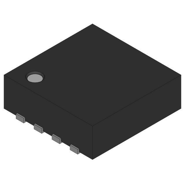
The LM4570 is available in an 8-pin WSON package which features an exposed DAP (die attach paddle). The
exposed DAP provides a direct thermal conduction path between the die and the PCB, improving the thermal
performance by reducing the thermal resistance of the package. Connect the exposed DAP to GND through a
large pad beneath the device, and multiple vias to a large unbroken GND plane. For best thermal performance,
connect the DAP pad to a GND plane on an outside layer of the PCB. Connecting the DAP to a plane on an
inner layer will result in a higher thermal resistance. Ensure efficient thermal conductivity by plugging and tenting
the vias with plating and solder mask, respectively.
POWER SUPPLY BYPASSING
Good power supply bypassing is critical for proper operation. Locate both the REF1 and VDD bypass capacitors
as close to the device as possible. Typical applications employ a regulator with a 10µF tantalum or electrolytic
capacitor and a ceramic bypass capacitor which aid in supply stability. This does not eliminate the need for
bypass capacitors near the LM4570. Place a 1µF ceramic capacitor as close to VDD as possible. Place a 0.1µF
capacitor as close to REF1 as possible. Smaller values of CREF1 may be chosen for decreased turn on times.
SHUTDOWN FUNCTION
The LM4570 features a low power shutdown mode that disables the device and reduces quiescent current
consumption to 0.1µA. Driving /SD Low disables the amplifiers and bias circuitry, and drives VREF1and the
outputs to GND. Connect /SD to VDD for normal operation.
8
Submit Documentation Feedback
Copyright © 2006–2013, Texas Instruments Incorporated
Product Folder Links: LM4570
�LM4570
www.ti.com
SNOSAV2C – APRIL 2006 – REVISED APRIL 2013
DEMO BOARD LAYOUT
C1
1 PF
5
R3
VDD
20 k:
C2
R2
IN
MOTOR
CONTROL SIGNAL
3
REF2
2
20 k:
SHORT
0:
C3
REF1
1
VO1
4
LM4570
0.1 PF
VO2
ON
/SD
OFF
7
8
R1
GND
6
OPEN
Revision History
Rev
Date
Description
1.0
04/13/06
Initial release.
1.01
07/28/09
Added the Ordering Information table.
C
04/08/13
Changed layout of National Data Sheet to TI format.
Submit Documentation Feedback
Copyright © 2006–2013, Texas Instruments Incorporated
Product Folder Links: LM4570
9
�PACKAGE OPTION ADDENDUM
www.ti.com
10-Dec-2020
PACKAGING INFORMATION
Orderable Device
Status
(1)
Package Type Package Pins Package
Drawing
Qty
Eco Plan
(2)
Lead finish/
Ball material
MSL Peak Temp
Op Temp (°C)
Device Marking
(3)
(4/5)
(6)
LM4570LQ/NOPB
ACTIVE
WQFN
NGP
8
1000
RoHS & Green
SN
Level-3-260C-168 HR
-40 to 85
GC8
(1)
The marketing status values are defined as follows:
ACTIVE: Product device recommended for new designs.
LIFEBUY: TI has announced that the device will be discontinued, and a lifetime-buy period is in effect.
NRND: Not recommended for new designs. Device is in production to support existing customers, but TI does not recommend using this part in a new design.
PREVIEW: Device has been announced but is not in production. Samples may or may not be available.
OBSOLETE: TI has discontinued the production of the device.
(2)
RoHS: TI defines "RoHS" to mean semiconductor products that are compliant with the current EU RoHS requirements for all 10 RoHS substances, including the requirement that RoHS substance
do not exceed 0.1% by weight in homogeneous materials. Where designed to be soldered at high temperatures, "RoHS" products are suitable for use in specified lead-free processes. TI may
reference these types of products as "Pb-Free".
RoHS Exempt: TI defines "RoHS Exempt" to mean products that contain lead but are compliant with EU RoHS pursuant to a specific EU RoHS exemption.
Green: TI defines "Green" to mean the content of Chlorine (Cl) and Bromine (Br) based flame retardants meet JS709B low halogen requirements of


 工商网监
湘ICP备2023018690号
工商网监
湘ICP备2023018690号
