LM48411
www.ti.com
LM48411
SNAS399G – SEPTEMBER 2007 – REVISED MAY 2013
Ultra-Low EMI, Filterless, 2.5W, Stereo, Class D
Audio Power Amplifier with E2S
Check for Samples: LM48411
FEATURES
1
•
2
•
•
•
•
•
•
•
•
•
2
E S System Reduces EMI Preserving Audio
Quality and Efficiency
Output Short Circuit Protection
Stereo Class D Operation
No Output Filter Required for Inductive Loads
Logic Selectable Gain
Independent Shutdown Control
Minimum External Components
"Click and Pop" Suppression Circuitry
Micro-Power Shutdown Mode
Available in Space-Saving 0.5mm Pitch
DSBGA Package
APPLICATIONS
•
•
•
Mobile Phones
PDAs
Portable Electronic Devices
KEY SPECIFICATIONS
•
•
•
•
•
•
•
•
Efficiency at 3.6V, 500mW into 8Ω Speaker:
87% (typ)
Efficiency at 3.6V, 100mW into 8Ω Speaker:
80% (typ)
Efficiency at 5V, 1W into 8Ω Speaker:
88% (typ)
Quiescent Current, 3.6V Supply: 4.2mA (typ)
Power Output at VDD = 5V RL = 4Ω, THD ≤ 10%:
2.5W (typ)
Power Output at VDD = 5V RL = 8Ω, THD ≤ 10%:
1.5W (typ)
Total Shutdown Power Supply Current:
0.01µA (typ)
Single Supply Range: 2.4V to 5.5V
DESCRIPTION
The LM48411 is a single supply, high efficiency,
2.5W/channel Class D audio amplifier. The LM48411
features TI's Enhanced Emissions Suppression (E2S)
system, that features a unique patent-pending ultra
low EMI, spread spectrum, PWM architecture, that
significantly reduces RF emissions while preserving
audio quality and efficiency. The E2S system
improves battery life, reduces external component
count, board area consumption, system cost, and
simplifying design.
The LM48411 is designed to meet the demands of
mobile phones and other portable communication
devices. Operating on a single 5V supply, it is
capable of delivering 2.5W/channel of continuous
output power to a 4Ω load with less than 10%
THD+N. Its flexible power supply requirements allow
operation from 2.4V to 5.5V. The wide band spread
spectrum architecture of the LM48411 reduces EMIradiated emissions due to the modulator frequency.
The LM48411 features high efficiency compared to a
conventional Class AB amplifier. The E2S system
includes an advanced, patent-pending edge rate
control (ERC) architecture that further reduce
emissions by minimizing the high frequency
component of the device output, while maintaining
high quality audio reproduction and high efficiency (η
= 87% at VDD = 3.6V, PO = 500mW). Four gain
options are pin selectable through GAIN0 and GAIN1
pins.
The LM48411 features a low-power consumption
shutdown mode. Shutdown may be enabled by
driving the Shutdown pin to a logic low (GND).
Output short circuit protection prevents the device
from being damaged during fault conditions. Superior
click and pop suppression eliminates audible
transients on power up/down and during shutdown.
Independent left/right shutdown control maximizes
power savings in mixed mono/stereo applications.
1
2
Please be aware that an important notice concerning availability, standard warranty, and use in critical applications of
Texas Instruments semiconductor products and disclaimers thereto appears at the end of this data sheet.
All trademarks are the property of their respective owners.
PRODUCTION DATA information is current as of publication date.
Products conform to specifications per the terms of the Texas
Instruments standard warranty. Production processing does not
necessarily include testing of all parameters.
Copyright © 2007–2013, Texas Instruments Incorporated
�LM48411
SNAS399G – SEPTEMBER 2007 – REVISED MAY 2013
www.ti.com
LM48411 RF Emissions
50.0
FCC Class B Limit
AMPLITUDE (dBPV/m)
45.0
40.0
35.0
30.0
LM48411TL Output Spectrum
25.0
20.0
15.0
10.0
30.0
80.0 120.0 160.0 200.0 240.0 280.0
FREQUENCY (MHz)
Figure 1. RF Emissions — 3in cable
Typical Application
2.4V to 5.5V
CS2
CS1
VDD
AUDIO
INPUT
PVDD
Ci
INR+
OUTRA
GAIN/
MODULATOR
Ci
H-BRIDGE
INR-
OUTRB
SDR
GAIN0
OSCILLATOR
GAIN1
SDL
AUDIO
INPUT
Ci
INL+
OUTLA
GAIN/
MODULATOR
Ci
H-BRIDGE
INL-
OUTLB
GND
PGND
Figure 2. Typical Audio Amplifier Application Circuit
2
Submit Documentation Feedback
Copyright © 2007–2013, Texas Instruments Incorporated
Product Folder Links: LM48411
�LM48411
www.ti.com
SNAS399G – SEPTEMBER 2007 – REVISED MAY 2013
Connection Diagram
4
OUTRB
OUTRA
AVDD
INR+
3
PGND
AGND
G0
INR-
2
SDL
SDR
G1
INL-
1
OUTLB
OUTLA
PVDD
INL+
C
D
A
B
Figure 3. DSBGA - Top View
See YZR0016 Package
PIN DESCRIPTIONS
Bump
Name
A1
OUTLB
Function
Left Channel output B
A2
SDL
A3
PGND
Left channel active low shutdown
Power GND
A4
OUTRB
Right channel output B
B1
OUTLA
Left channel output A
B2
SDR
B3
AGND
Ground
Right channel output A
Right channel active low shutdown
B4
OUTRA
C1
PVDD
C2
G1
Gain setting input 1
C3
G0
Gain setting input 0
C4
AVDD
Power supply
D1
INL+
Non-inverting left channel input
D2
INL-
Inverting left channel input
D3
INR-
Inverting right channel input
D4
INR+
Non-inverting right channel input
Power VDD
These devices have limited built-in ESD protection. The leads should be shorted together or the device placed in conductive foam
during storage or handling to prevent electrostatic damage to the MOS gates.
Submit Documentation Feedback
Copyright © 2007–2013, Texas Instruments Incorporated
Product Folder Links: LM48411
3
�LM48411
SNAS399G – SEPTEMBER 2007 – REVISED MAY 2013
www.ti.com
Absolute Maximum Ratings (1) (2) (3)
Supply Voltage (1)
6.0V
−65°C to +150°C
Storage Temperature
VDD + 0.3V ≥ V ≥ GND - 0.3V
Voltage at Any Input Pin
Power Dissipation (4)
ESD Rating, all other pins
Internally Limited
(5)
2.0kV
ESD Rating (6)
200V
Junction Temperature (TJMAX)
Thermal Resistance
150°C
θJA (DSBGA)
Soldering Information
(1)
(2)
(3)
(4)
(5)
(6)
63.6°C/W
See SNVA009 "microSMD Wafers Level Chip Scale Package."
“Absolute Maximum Ratings” indicate limits beyond which damage to the device may occur, including inoperability and degradation of
device reliability and/or performance. Functional operation of the device and/or non-degradation at the Absolute Absolute Maximum
Ratings or other conditions beyond those indicated in the Recommended Operating Conditions is not implied. The Recommended
Operating Conditions indicate conditions at which the device is functional and the device should not be operated beyond such
conditions. All voltages are measured with respect to the ground pin, unless otherwise specified
The Electrical Characteristics tables list ensured specifications under the listed Recommended Operating Conditions except as
otherwise modified or specified by the Electrical Characteristics Conditions and/or Notes. Typical specifications are estimations only and
are not ensured.
If Military/Aerospace specified devices are required, please contact the TI Sales Office/ Distributors for availability and specifications.
The maximum power dissipation must be derated at elevated temperatures and is dictated by TJMAX, θJA, and the ambient temperature,
TA. The maximum allowable power dissipation is PDMAX = (TJMAX - TA) / θJA or the number given in Absolute Maximum Ratings,
whichever is lower. For the LMxxxxx, see Power Derating curves for additional information.
Human body model, applicable std. JESD22-A114C.
Machine model, applicable std. JESD22-A115-A.
Operating Ratings (1) (2)
Temperature Range TMIN ≤ TA ≤ TMAX
−40°C ≤ TA ≤ 85°C
2.4V ≤ VDD ≤ 5.5V
Supply Voltage
(1)
(2)
4
“Absolute Maximum Ratings” indicate limits beyond which damage to the device may occur, including inoperability and degradation of
device reliability and/or performance. Functional operation of the device and/or non-degradation at the Absolute Absolute Maximum
Ratings or other conditions beyond those indicated in the Recommended Operating Conditions is not implied. The Recommended
Operating Conditions indicate conditions at which the device is functional and the device should not be operated beyond such
conditions. All voltages are measured with respect to the ground pin, unless otherwise specified
The Electrical Characteristics tables list ensured specifications under the listed Recommended Operating Conditions except as
otherwise modified or specified by the Electrical Characteristics Conditions and/or Notes. Typical specifications are estimations only and
are not ensured.
Submit Documentation Feedback
Copyright © 2007–2013, Texas Instruments Incorporated
Product Folder Links: LM48411
�LM48411
www.ti.com
SNAS399G – SEPTEMBER 2007 – REVISED MAY 2013
Electrical Characteristics
The following specifications apply for AV = 6dB, RL = 15μH+8Ω, f = 1kHz, unless otherwise specified. Limits apply for TA =
25°C. VDD = 3.6V.
Symbol
|VOS|
IDD
Parameter
Differential Output Offset Voltage
Quiescent Power Supply Current
Conditions
VI = 0V, AV = 2V/V,
VDD = 2.4V to 5.0V
LM48411
Typical (1)
5
5.1
7.5
mA (max)
4.2
6.0
mA (max)
VIN = 0V, No Load, VDD = 2.4V
3.0
4.5
mA (max)
VIN = 0V, RL = 8Ω, VDD = 5.0V
5.2
mA
VIN = 0V, RL = 8Ω, VDD = 3.6V
4.2
mA
VIN = 0V, RL = 8Ω, VDD = 2.4V
3.0
VSDR = VSDL= GND
0.01
VSDIH
Shutdown voltage input high
VSDIL
Shutdown voltage input low
RIN
TWU
(1)
(2)
(3)
Input Resistance
Wake Up Time
mV
VIN = 0V, No Load, VDD = 3.6V
Shutdown Current (3)
Gain
Units
(Limits)
VIN = 0V, No Load, VDD = 5.0V
ISD
AV
Limit (2) (3)
mA
1.0
μA (max)
For SDR, SDL
1.4
V (min)
For SDR, SDL
0.4
V (max)
GAIN0, GAIN1 = GND
RL = ∞
6
6±0.5
dB
GAIN0 = VDD, GAIN1 = GND
RL = ∞
12
12±0.5
dB
GAIN0 = GND, GAIN1 = VDD
RL = ∞
18
18±0.5
dB
GAIN0, GAIN1 = VDD
RL = ∞
24
24±0.5
dB
AV = 6dB
56
kΩ
AV = 12dB
37.5
kΩ
AV = 18dB
22.5
kΩ
AV = 24dB
12.5
kΩ
VSDR/SDL = 0.4V
4.2
ms
Typical values represent most likely parametric norms at TA = +25ºC, and at the Recommended Operation Conditions at the time of
product characterization and are not specified.
Datasheet min/max specification limits are not specified by test or statistical analysis.
Shutdown current is measured in a normal room environment. Exposure to direct sunlight will increase ISD by a maximum of 2µA. The
Shutdown pin should be driven as close as possible to GND for minimal shutdown current and to VDD for the best THD performance in
PLAY mode. See the Application Information section under SHUTDOWN FUNCTION for more information.
Submit Documentation Feedback
Copyright © 2007–2013, Texas Instruments Incorporated
Product Folder Links: LM48411
5
�LM48411
SNAS399G – SEPTEMBER 2007 – REVISED MAY 2013
www.ti.com
Electrical Characteristics (continued)
The following specifications apply for AV = 6dB, RL = 15μH+8Ω, f = 1kHz, unless otherwise specified. Limits apply for TA =
25°C. VDD = 3.6V.
Symbol
Parameter
Conditions
LM48411
Typical (1)
Limit (2) (3)
Units
(Limits)
RL = 15μH + 4Ω + 15μH
THD = 10% (max)
f = 1kHz, 22kHz BW
VDD = 5V
2.5
W
VDD = 3.6V
1.2
W
VDD = 2.5V
530
mW
VDD = 5V
2
W
VDD = 3.6V
1
W
VDD = 2.5V
430
mW
RL = 15μH + 4Ω + 15μH
THD = 1% (max)
f = 1kHz, 22kHz BW
PO
Output Power
RL = 15μH + 8Ω + 15μH
THD = 10% (max)
f = 1kHz, 22kHz BW
VDD = 5V
1.5
W
VDD = 3.6V
760
mW
VDD = 2.5V
330
mW
VDD = 5V
1.25
W
VDD = 3.6V
615
mW
VDD = 2.5V
270
mW
PO = 500mW, f = 1kHz, RL = 8Ω
0.05
%
PO = 300mW, f = 1kHz, RL = 8Ω
RL = 15μH + 8Ω + 15μH
THD = 1% (max)
f = 1kHz, 22kHz BW
THD+N
PSRR
Total Harmonic Distortion + Noise
Power Supply Rejection Ratio
(Input Referred)
0.03
%
VRipple = 200mVPP Sine,
fRipple = 217Hz, VDD = 3.6, 5V
Inputs to AC GND, CI = 2μF
78
dB
VRipple = 200mVPP Sine,
fRipple = 1kHz, VDD = 3.6, 5V
Inputs to AC GND, CI = 2μF
77
dB
SNR
Signal to Noise Ratio
VDD = 5V, PO = 1WRMS
96
dB
εOUT
Output Noise
(Input Referred)
VDD = 3.6V, A Weighted
22
μVRMS
CMRR
Common Mode Rejection Ratio
(Input Referred)
VDD = 3.6V, VRipple = 1VPP Sine
fRipple = 217Hz
64
dB
η
Efficiency
VDD = 5V, POUT = 1W
RL = 8Ω
88
%
Xtalk
Crosstalk
PO = 500mW, f = kHz
84
dB
6
Submit Documentation Feedback
Copyright © 2007–2013, Texas Instruments Incorporated
Product Folder Links: LM48411
�LM48411
www.ti.com
SNAS399G – SEPTEMBER 2007 – REVISED MAY 2013
Typical Performance Characteristics
The performance graphs were taken using the Audio Precision AUX-0025 Switching Amplifier measurement Filter in series
with the LC filter on the demo board.
THD+N vs Frequency
VDD = 3.6V, RL = 8Ω, PO = 250mW/channel
AV = 6dB
10
10
1
1
THD+N (%)
THD+N (%)
THD+N vs Frequency
VDD = 2.5V, RL = 8Ω, PO = 100mW/channel
AV = 6dB
0.1
0.01
0.01
0.001
20
0.1
100
1k
0.001
20
10k 20k
100
Figure 5.
THD+N vs Frequency
VDD = 5.0V, RL = 8Ω, PO = 375mW/channel
AV = 6dB
THD+N vs Frequency
VDD = 2.5V, RL = 4Ω, PO = 100mW/channel
AV = 6dB
10
10
1
1
THD+N (%)
THD+N (%)
10k 20k
Figure 4.
0.1
0.001
20
0.1
0.01
0.01
100
1k
0.001
20
10k 20k
100
FREQUENCY (Hz)
1k
10k 20k
FREQUENCY (Hz)
Figure 6.
Figure 7.
THD+N vs Frequency
VDD = 3.6V, RL = 4Ω, PO = 250mW/channel
AV = 6dB
THD+N vs Frequency
VDD = 5.0V, RL = 4Ω, PO = 375mW/channel
AV = 6dB
10
10
1
1
THD+N (%)
THD+N (%)
1k
FREQUENCY (Hz)
FREQUENCY (Hz)
0.1
0.01
0.01
0.001
20
0.1
100
1k
10k 20k
FREQUENCY (Hz)
0.001
20
100
1k
10k 20k
FREQUENCY (Hz)
Figure 8.
Figure 9.
Submit Documentation Feedback
Copyright © 2007–2013, Texas Instruments Incorporated
Product Folder Links: LM48411
7
�LM48411
SNAS399G – SEPTEMBER 2007 – REVISED MAY 2013
www.ti.com
Typical Performance Characteristics (continued)
The performance graphs were taken using the Audio Precision AUX-0025 Switching Amplifier measurement Filter in series
with the LC filter on the demo board.
THD+N vs Output Power
VDD = 2.5V, RL = 8Ω, AV = 24dB
10
10
1
1
THD+N (%)
THD+N (%)
THD+N vs Output Power
VDD = 2.5V, RL = 8Ω, AV = 6dB
0.1
0.1
0.01
0.01
0.001
10m
100m
0.001
10m
1
Figure 11.
THD+N vs Output Power
VDD = 3.6V, RL = 8Ω, AV = 6dB
THD+N vs Output Power
VDD = 3.6V, RL = 8Ω, AV = 24dB
10
10
1
1
THD+N (%)
THD+N (%)
Figure 10.
0.1
0.01
0.001
10m
0.1
0.01
100m
0.001
10m
1
OUTPUT POWER (W)
1
OUTPUT POWER (W)
Figure 13.
THD+N vs Output Power
VDD = 5V, RL = 8Ω, AV = 6dB
THD+N vs Output Power
VDD = 5V, RL = 8Ω, AV = 24dB
10
THD+N (%)
0.1
0.1
0.01
0.01
0.001
10m
100m
Figure 12.
10
THD+N (%)
1
OUTPUT POWER (W)
OUTPUT POWER (W)
100m
1
2
0.001
10m
100m
1
2
OUTPUT POWER (W)
OUTPUT POWER (W)
Figure 14.
8
100m
Figure 15.
Submit Documentation Feedback
Copyright © 2007–2013, Texas Instruments Incorporated
Product Folder Links: LM48411
�LM48411
www.ti.com
SNAS399G – SEPTEMBER 2007 – REVISED MAY 2013
Typical Performance Characteristics (continued)
The performance graphs were taken using the Audio Precision AUX-0025 Switching Amplifier measurement Filter in series
with the LC filter on the demo board.
THD+N vs Output Power
VDD = 2.5V, RL = 4Ω, AV = 24dB
10
10
1
1
THD+N (%)
THD+N (%)
THD+N vs Output Power
VDD = 2.5V, RL = 4Ω, AV = 6dB
0.1
0.01
0.1
0.01
0.001
10m
100m
0.001
10m
1
OUTPUT POWER (W)
Figure 17.
THD+N vs Output Power
VDD = 3.6V, RL = 4Ω, AV = 6dB
THD+N vs Output Power
VDD = 3.6V, RL = 4Ω, AV = 24dB
10
10
1
1
0.1
0.01
0.1
0.01
0.001
10m
1
100m
0.001
10m
2
OUTPUT POWER (W)
1
100m
2
OUTPUT POWER (W)
Figure 18.
Figure 19.
THD+N vs Output Power
VDD = 5.0V, RL = 4Ω, AV = 6dB
THD+N vs Output Power
VDD = 5.0V, RL = 4Ω, AV = 24dB
10
10
1
1
THD+N (%)
THD+N (%)
1
Figure 16.
THD+N (%)
THD+N (%)
OUTPUT POWER (W)
100m
0.1
0.01
0.001
10m
0.1
0.01
100m
1
2
3
OUTPUT POWER (W)
0.001
10m
100m
1
2
3
OUTPUT POWER (W)
Figure 20.
Figure 21.
Submit Documentation Feedback
Copyright © 2007–2013, Texas Instruments Incorporated
Product Folder Links: LM48411
9
�LM48411
SNAS399G – SEPTEMBER 2007 – REVISED MAY 2013
www.ti.com
Typical Performance Characteristics (continued)
The performance graphs were taken using the Audio Precision AUX-0025 Switching Amplifier measurement Filter in series
with the LC filter on the demo board.
PSRR vs Frequency
VDD = 3.6V, RL = 8Ω
CMRR vs Frequency
VDD = 3.6V, RL = 8Ω
0
0
-10
-10
-20
-20
-30
CMRR (dB)
PSRR (dB)
-30
-40
-50
-40
-50
-60
-60
-70
-70
-80
-90
-80
-90
20
10k 20k
100
1k
FREQUENCY (Hz)
100 200
1k 2k
10k 20k
FREQUENCY (Hz)
Figure 22.
Figure 23.
Quiescent Current vs Power Supply
RL = ∞
Output Power vs Supply Voltage
RL = 4Ω, f = 1kHz
3000
5
2500
OUTPUT POWER (mW)
6
4
QCURR (mA)
-100
20
3
2
1
2000
THD+N=10%
1500
1000
THD+N=1%
500
0
2.0
2.5
3.0
3.5
4.0
4.5
5.0
5.5
0
2.5
POWER SUPPLY (V)
3.0
3.5
4.0
4.5
5.0
5.5
SUPPLY VOLTAGE (V)
Figure 24.
Figure 25.
Output Power vs Supply Voltage
RL = 8Ω, f = 1kHz
100
2000
Efficiency vs Output Power
RL = 4Ω
90
1000
EFFCIENCY (%)
OUTPUT POWER (mW)
80
1500
THD+N=10%
THD+N=1%
VDD = 5.0V
70
VDD = 3.6V
60
VDD = 2.5V
50
40
30
20
500
10
0
0
0
2.5
3.0
3.5
4.0
4.5
5.0
5.5
0.5
1.0
1.5
2.0
2.5
OUTPUT POWER (W)
SUPPLY VOLTAGE (V)
Figure 26.
10
Figure 27.
Submit Documentation Feedback
Copyright © 2007–2013, Texas Instruments Incorporated
Product Folder Links: LM48411
�LM48411
www.ti.com
SNAS399G – SEPTEMBER 2007 – REVISED MAY 2013
Typical Performance Characteristics (continued)
The performance graphs were taken using the Audio Precision AUX-0025 Switching Amplifier measurement Filter in series
with the LC filter on the demo board.
100
Efficiency vs Output Power
RL = 8Ω
Crosstalk vs Frequency
VDD = 3.6V, RL = 8Ω
0
90
-10
VDD = 5.0V
70
-20
VDD = 3.6V
60
-30
CROSSTALK (dB)
EFFCIENCY (%)
80
VDD = 2.5V
50
40
30
20
-40
-50
-60
-70
10
-80
0
0
0.2
0.4
0.6
0.8
1.0
-90
1.2
-100
20
OUTPUT POWER (W)
100 200
1k 2k
10k 20k
FREQUENCY (Hz)
Figure 28.
Figure 29.
Power Dissipation vs Output Power
RL = 4Ω
Power Dissipation vs Output Power
RL = 8Ω
1.40
0.50
0.45
1.00
0.80
0.60
VDD = 5.0V
VDD = 2.5V
0.40
POWER DISSIPATION (W)
POWER DISSIPATION (w)
1.20
0.20
0.5
1.0
1.5
2.0 2.5
VDD = 5.0V
0.35
0.30
0.25
0.20
0.15
VDD = 3.6V
0.10
0.05
VDD = 3.6V
0.00
0.0
0.40
3.0
3.5
4.0
0.00
0.0
VDD = 2.5V
1.0
2.0
3.0
4.0
5.0
OUTPUT POWER (W)
OUTPUT POWER (W)
Figure 30.
Figure 31.
Submit Documentation Feedback
Copyright © 2007–2013, Texas Instruments Incorporated
Product Folder Links: LM48411
11
�LM48411
SNAS399G – SEPTEMBER 2007 – REVISED MAY 2013
www.ti.com
External Components Description
(Figure 2)
Components
Functional Description
1.
CS
Supply bypass capacitor which provides power supply filtering. Refer to the Power Supply Bypassing section for
information concerning proper placement and selection of the supply bypass capacitor.
2.
CI
Input AC coupling capacitor which blocks the DC voltage at the amplifier's input terminals.
APPLICATION INFORMATION
GENERAL AMPLIFIER FUNCTION
The LM48411 features a filterless modulation scheme. The differential outputs of the device switch at 300kHz
from VDD to GND. When there is no input signal applied, the two outputs (VO1 and VO2) switch with a 50% duty
cycle, with both outputs in phase. Because the outputs of the LM48411 are differential, the two signals cancel
each other. This results in no net voltage across the speaker, thus there is no load current during an idle state,
conserving power.
With an input signal applied, the duty cycle (pulse width) of the LM48411 outputs changes. For increasing output
voltages, the duty cycle of VO1 increases, while the duty cycle of VO2 decreases. For decreasing output voltages,
the converse occurs, the duty cycle of VO2 increases while the duty cycle of VO1 decreases. The difference
between the two pulse widths yields the differential output voltage.
SPREAD SPECTRUM MODULATION
The LM48411 features a fitlerless spread spectrum modulation scheme that eliminates the need for output filters,
ferrite beads or chokes. The switching frequency varies by ±30% about a 300kHz center frequency, reducing the
wideband spectral contend, improving EMI emissions radiated by the speaker and associated cables and traces.
Where a fixed frequency class D exhibits large amounts of spectral energy at multiples of the switching
frequency, the spread spectrum architecture of the LM48411 spreads that energy over a larger bandwidth. The
cycle-to-cycle variation of the switching period does not affect the audio reproduction of efficiency.
ENHANCED EMISSIONS SUPPRESSION SYSTEM (E2S)
The LM48411 features TI’s patent-pending E2S system that reduces EMI, while maintaining high quality audio
reproduction and efficiency. The E2S system features a synchronizable oscillator with selectable spread
spectrum, and advanced edge rate control (ERC). The LM48411 ERC greatly reduces the high frequency
components of the output square waves by controlling the output rise and fall times, slowing the transitions to
reduce RF emissions, while maximizing THD+N and efficiency performance.
POWER DISSIPATION AND EFFICIENCY
In general terms, efficiency is considered to be the ratio of useful work output divided by the total energy required
to produce it with the difference being the power dissipated, typically, in the IC. The key here is “useful” work. For
audio systems, the energy delivered in the audible bands is considered useful including the distortion products of
the input signal. Sub-sonic (DC) and super-sonic components (>22kHz) are not useful. The difference between
the power flowing from the power supply and the audio band power being transduced is dissipated in the
LM48411 and in the transducer load. The amount of power dissipation in the LM48411 is very low. This is
because the ON resistance of the switches used to form the output waveforms is typically less than 0.25Ω. This
leaves only the transducer load as a potential "sink" for the small excess of input power over audio band output
power. The LM48411 dissipates only a fraction of the excess power requiring no additional PCB area or copper
plane to act as a heat sink.
DIFFERENTIAL AMPLIFIER EXPLANATION
As logic supply voltages continue to shrink, designers are increasingly turning to differential analog signal
handling to preserve signal to noise ratios with restricted voltage swing. The LM48411 is a fully differential
amplifier that features differential input and output stages. A differential amplifier amplifies the difference between
the two input signals. Traditional audio power amplifiers have typically offered only single-ended inputs resulting
in a 6dB reduction in signal to noise ratio relative to differential inputs. The LM48411 also offers the possibility of
12
Submit Documentation Feedback
Copyright © 2007–2013, Texas Instruments Incorporated
Product Folder Links: LM48411
�LM48411
www.ti.com
SNAS399G – SEPTEMBER 2007 – REVISED MAY 2013
DC input coupling which eliminates the two external AC coupling, DC blocking capacitors. The LM48411 can be
used, however, as a single ended input amplifier while still retaining it's fully differential benefits. In fact,
completely unrelated signals may be placed on the input pins. The LM48411 simply amplifies the difference
between the signals. A major benefit of a differential amplifier is the improved common mode rejection ratio
(CMRR) over single input amplifiers. The common-mode rejection characteristic of the differential amplifier
reduces sensitivity to ground offset related noise injection, especially important in high noise applications.
PCB LAYOUT CONSIDERATIONS
As output power increases, interconnect resistance (PCB traces and wires) between the amplifier, load and
power supply create a voltage drop. The voltage loss on the traces between the LM48411 and the load results is
lower output power and decreased efficiency. Higher trace resistance between the supply and the LM48411 has
the same effect as a poorly regulated supply, increased ripple on the supply line also reducing the peak output
power. The effects of residual trace resistance increases as output current increases due to higher output power,
decreased load impedance or both. To maintain the highest output voltage swing and corresponding peak output
power, the PCB traces that connect the output pins to the load and the supply pins to the power supply should
be as wide as possible to minimize trace resistance.
The use of power and ground planes will give the best THD+N performance. While reducing trace resistance, the
use of power planes also creates parasite capacitors that help to filter the power supply line.
The inductive nature of the transducer load can also result in overshoot on one or both edges, clamped by the
parasitic diodes to GND and VDD in each case. From an EMI standpoint, this is an aggressive waveform that can
radiate or conduct to other components in the system and cause interference. It is essential to keep the power
and output traces short and well shielded if possible. Use of ground planes, beads, and micro-strip layout
techniques are all useful in preventing unwanted interference.
As the distance from the LM48411 and the speaker increase, the amount of EMI radiation will increase since the
output wires or traces acting as antenna become more efficient with length. What is acceptable EMI is highly
application specific. Ferrite chip inductors placed close to the LM48411 may be needed to reduce EMI radiation.
The value of the ferrite chip is very application specific.
SHUTDOWN FUNCTION
In order to reduce power consumption while not in use, the LM48411 contains shutdown circuitry that reduces
current draw to less than 0.01µA. The trigger point for shutdown is shown as a typical value in the Electrical
Characteristics Tables and in the Shutdown Hysteresis Voltage graphs found in the Typical Performance
Characteristics section. It is best to switch between ground and supply for minimum current usage while in the
shutdown state. While the LM48411 may be disabled with shutdown voltages in between ground and supply, the
idle current will be greater than the typical 0.01µA value.
The LM48411 has an internal resistor connected between GND and Shutdown pins. The purpose of this resistor
is to eliminate any unwanted state changes when the Shutdown pin is floating. The LM48411 will enter the
shutdown state when the Shutdown pin is left floating or if not floating, when the shutdown voltage has crossed
the threshold. To minimize the supply current while in the shutdown state, the Shutdown pin should be driven to
GND or left floating. If the Shutdown pin is not driven to GND, the amount of additional resistor current due to the
internal shutdown resistor can be found by Equation 1 below.
(VSD - GND) / 300kΩ
(1)
With only a 0.5V difference, an additional 1.7µA of current will be drawn while in the shutdown state.
AUDIO AMPLIFIER POWER SUPPLY BYPASSING FILTERING
Proper power supply bypassing is critical for low noise performance and high PSRR. Place the supply bypass
capacitor as close to the device as possible. Typical applications employ a voltage regulator with 10µF and 0.1µF
bypass capacitors that increase supply stability. These capacitors do not eliminate the need for bypassing of the
LM48411 supply pins. A 1µF capacitor is recommended.
Submit Documentation Feedback
Copyright © 2007–2013, Texas Instruments Incorporated
Product Folder Links: LM48411
13
�LM48411
SNAS399G – SEPTEMBER 2007 – REVISED MAY 2013
www.ti.com
AUDIO AMPLIFIER INPUT CAPACITOR SELECTION
Input capacitors may be required for some applications, or when the audio source is single-ended. Input
capacitors block the DC component of the audio signal, eliminating any conflict between the DC component of
the audio source and the bias voltage of the LM48411. The input capacitors create a high-pass filter with the
input resistance Ri. The -3dB point of the high pass filter is found using Equation 2 below.
f = 1 / 2πRiCi
(2)
The values for Ri can be found in the EC table for each gain setting.
The input capacitors can also be used to remove low frequency content from the audio signal. Small speakers
cannot reproduce, and may even be damaged by low frequencies. High pass filtering the audio signal helps
protect the speakers. When the LM48411 is using a single-ended source, power supply noise on the ground is
seen as an input signal. Setting the high-pass filter point above the power supply noise frequencies, 217 Hz in a
GSM phone, for example, filters out the noise such that it is not amplified and heard on the output. Capacitors
with a tolerance of 10% or better are recommended for impedance matching and improved CMRR and PSRR.
AUDIO AMPLIFIER GAIN SETTING
The LM48411 features four internally configured gain settings. The device gain is selected through the two logic
inputs, G0 and G1. The gain settings are as shown in the following table.
LOGIC INPUT
GAIN
G1
G0
V/V
0
0
2
dB
6
0
1
4
12
1
0
8
18
1
1
16
24
Build of Materials
Designator
14
Footprint
Quantity
C1, C2
Ceramic Capacitor 0.1μF, 50V, 10%
Description
805
2
C3 – C6
Tantalum Capacitors 1μF 20V, 10%, Size A
1206
4
C11
Tantalum Capacitors 10μF 20V, 10% Size B
1411
1
JP1–5, JP8–11
Jumper Header Vertical Mount 2X1 0.100
9
JP6, JP7
Jumper Header Vertical Mount 3x1 0.100
2
Submit Documentation Feedback
Copyright © 2007–2013, Texas Instruments Incorporated
Product Folder Links: LM48411
�LM48411
www.ti.com
SNAS399G – SEPTEMBER 2007 – REVISED MAY 2013
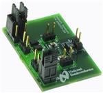
Demonstration Board Schematic
JP1
JP6
VDD
C1
1 PF
SDR
1
2
VDD
INR-
VDD
PVDD
INR+
INR+
C4
1 PF
+
1
2
3
C3
1 PF
JP2
INRJP8
GAIN0
SDR
OUTRA
SDR
OUTRB
1
2
3
VDD
GAIN0
GAIN1
GAIN1
SDL
GAIN1
JP3
1
2
C5
1 PF
INL+
INL-
SDL
1
2
JP9
OUTLA
SDL
OUTLB
1
2
INL+
C6
1 PF
+
JP5
1
2
GAIN0
+
JP7
C11
10 PF
+
VDD
C2
1 PF
+
JP4
1
2
VDD
1
2
INL-
GND
PGND
VDD
Demonstration Board Layout
Figure 32. Top Silkscreen Layer
Figure 33. Top Layer
Submit Documentation Feedback
Copyright © 2007–2013, Texas Instruments Incorporated
Product Folder Links: LM48411
15
�LM48411
SNAS399G – SEPTEMBER 2007 – REVISED MAY 2013
www.ti.com
Figure 34. Mid 1 Layer
Figure 35. Mid 2 Layer
Figure 36. Bottom Layer
16
Submit Documentation Feedback
Copyright © 2007–2013, Texas Instruments Incorporated
Product Folder Links: LM48411
�LM48411
www.ti.com
SNAS399G – SEPTEMBER 2007 – REVISED MAY 2013
REVISION HISTORY
Rev
Date
1.0
09/21/07
Initial release.
Description
1.1
10/01/07
Fixed few typos.
1.2
11/30/07
Added the demo boards and BOM.
1.3
12/19/07
Edited the 16–bump DSBGA package diagram and the Pin Description table.
1.4
01/08/08
Edited the 16–bump DSBGA package diagram.
1.5
06/27/08
Text edits.
1.6
07/03/08
Text edits (under SHUTDOWN FUNCTION).
Changes from Revision F (May 2013) to Revision G
•
Page
Changed layout of National Data Sheet to TI format .......................................................................................................... 16
Submit Documentation Feedback
Copyright © 2007–2013, Texas Instruments Incorporated
Product Folder Links: LM48411
17
�PACKAGE OPTION ADDENDUM
www.ti.com
10-Dec-2020
PACKAGING INFORMATION
Orderable Device
Status
(1)
Package Type Package Pins Package
Drawing
Qty
Eco Plan
(2)
Lead finish/
Ball material
MSL Peak Temp
Op Temp (°C)
Device Marking
(3)
(4/5)
(6)
LM48411TL/NOPB
ACTIVE
DSBGA
YZR
16
250
RoHS & Green
SNAGCU
Level-1-260C-UNLIM
-40 to 85
GJ2
LM48411TLX/NOPB
ACTIVE
DSBGA
YZR
16
3000
RoHS & Green
SNAGCU
Level-1-260C-UNLIM
-40 to 85
GJ2
(1)
The marketing status values are defined as follows:
ACTIVE: Product device recommended for new designs.
LIFEBUY: TI has announced that the device will be discontinued, and a lifetime-buy period is in effect.
NRND: Not recommended for new designs. Device is in production to support existing customers, but TI does not recommend using this part in a new design.
PREVIEW: Device has been announced but is not in production. Samples may or may not be available.
OBSOLETE: TI has discontinued the production of the device.
(2)
RoHS: TI defines "RoHS" to mean semiconductor products that are compliant with the current EU RoHS requirements for all 10 RoHS substances, including the requirement that RoHS substance
do not exceed 0.1% by weight in homogeneous materials. Where designed to be soldered at high temperatures, "RoHS" products are suitable for use in specified lead-free processes. TI may
reference these types of products as "Pb-Free".
RoHS Exempt: TI defines "RoHS Exempt" to mean products that contain lead but are compliant with EU RoHS pursuant to a specific EU RoHS exemption.
Green: TI defines "Green" to mean the content of Chlorine (Cl) and Bromine (Br) based flame retardants meet JS709B low halogen requirements of