LM48413
www.ti.com
SNAS460B – NOVEMBER 2008 – REVISED MARCH 2013
LM48413 Boomer™ Audio Power Amplifier Series Ultra Low EMI, Filterless, 1.2W Stereo
Class D Audio Power Amplifier with E2S and Texas Instruments 3D Enhancement
Check for Samples: LM48413
FEATURES
1
•
23
•
•
•
•
•
•
•
•
2
E S System Reduces EMI Preserving Audio
Quality and Efficiency
Output Short Circuit Protection
Stereo Class D Operation
No Output Filter Required
Texas Instruments 3D Enhancement
Minimum External Components
Click and Pop Suppression
Micro-Power Shutdown
Available in Space-Saving Approximately 2mm
x 2.2mm DSBGA Package
APPLICATIONS
•
•
•
Mobile Phones
PDAs
Laptops
KEY SPECIFICATIONS
•
•
•
•
•
•
Quiescent Power Supply Current at 3.6V
Supply 4mA (Typ)
Power Output at VDD = 5V, RL = 8Ω, THD ≤ 1%
1.2 W (Typ)
Shutdown Current 0.03µA (Typ)
Efficiency at 3.6V, 100mW into 8Ω 80% (Typ)
Efficiency at 3.6V, 500mW into 8Ω 80% (Typ)
Efficiency at 5V, 1W into 8Ω 86% (Typ)
DESCRIPTION
The LM48413 is a single supply, high efficiency,
1.2W/channel, filterless switching audio amplifier. The
LM48413 features Texas Instruments' Enhanced
Emissions Suppression (E2S) system - a unique
patented ultra low EMI, spread spectrum, PWM
architecture. It significantly reduces RF emission
while preserving audio quality and efficiency. The E2S
system improves battery life, reduces external
component count, board area consumption, system
cost and product design cycle time. The LM48413TL
is available in a micro-SMD package, further saving
space.
The LM48413 is designed to meet the demands of
mobile phones and other portable communication
devices. Operating from a single 5V supply, the
device is capable of delivering 1.2W/channel of
continuous output power to a 8Ω load with less than
1% THD+N. Flexible power supply requirements
allow operation from 2.4V to 5.5V. The wide band
spread spectrum architecture of the LM48413
reduces EMI-radiated emissions due to the modulator
frequency.
The LM48413 features high efficiency compared with
conventional Class AB amplifiers. The E2S system
includes an advanced, patent-pending edge rate
control (ERC) architecture that further reduce
emissions by minimizing the high frequency
components of the device output, while maintaining
its high quality audio reproduction and high efficiency
(η = 85% at VDD = 3.6V, PO = 500mW). The LM48413
also includes Texas Instruments' 3D audio
enhancement that improves stereo sound quality. In
devices where the left and right speakers are in close
proximity, 3D enhancement affects channel
specialization, widening the perceived soundstage.
Output short circuit protection prevents the device
from being damaged during fault conditions. Superior
click and pop suppression eliminates audible
transients on power up/down and during shutdown.
Shutdown control also provided to maximizes power
savings.
1
2
3
Please be aware that an important notice concerning availability, standard warranty, and use in critical applications of
Texas Instruments semiconductor products and disclaimers thereto appears at the end of this data sheet.
Boomer is a trademark of Texas Instruments.
All other trademarks are the property of their respective owners.
PRODUCTION DATA information is current as of publication date.
Products conform to specifications per the terms of the Texas
Instruments standard warranty. Production processing does not
necessarily include testing of all parameters.
Copyright © 2008–2013, Texas Instruments Incorporated
�LM48413
SNAS460B – NOVEMBER 2008 – REVISED MARCH 2013
www.ti.com
EMI Plot Using 6 inch Speaker Cables
Figure 1. EMI Radiation vs Frequency
VDD = 3V, RL = 15μH + 8Ω + 15μH
Typical Application
Figure 2. Typical Audio Amplifier Application Circuit
2
Submit Documentation Feedback
Copyright © 2008–2013, Texas Instruments Incorporated
Product Folder Links: LM48413
�LM48413
www.ti.com
SNAS460B – NOVEMBER 2008 – REVISED MARCH 2013
Connection Diagram
Figure 3. 18 bump DSBGA package
Top View
See Package Number YZR0018
BUMP DESCRIPTIONS
Bump
Name
A1
INL-
Description
Left Channel Inverting Input
A3
3DEN
A5
OUTLA
3D Enable Input
Left Channel Non-Inverting Output
A7
OUTLB
Left Channel Inverting Output
B2
INL+
Left Channel Non-Inverting Input
B4
3DL-
Left Channel inverting 3D connection. Connect to 3DR- through C3D-and R3D-
B6
GND
Ground
C1
3DL+
Left Channel non-inverting 3D connection. Connect to 3DR+ through C3D+ and R3D+
C3
3DR+
Right Channel non-inverting 3D connection. Connect to 3DL+ through C3D+ and R3D+
C5
VDD
C7
PGND
Power Supply. Connect to PVDD supplying same voltage.
D2
INR+
Right Channel Non-inverting Input
D4
3DR-
Right Channel inverting 3D connection. Connect to 3DL- through C3D-and R3D-
D6
PVDD
Amplifier Power Supply
E1
INR-
Right Channel Inverting Input
E3
SD
E5
OUTRA
Right Channel Non-inverting Output
E7
OUTRB
Right Channel Inverting Output
Power Ground
Connect to GND for disabling the device. Connect to VDD for normal operation.
These devices have limited built-in ESD protection. The leads should be shorted together or the device placed in conductive foam
during storage or handling to prevent electrostatic damage to the MOS gates.
Submit Documentation Feedback
Copyright © 2008–2013, Texas Instruments Incorporated
Product Folder Links: LM48413
3
�LM48413
SNAS460B – NOVEMBER 2008 – REVISED MARCH 2013
www.ti.com
Absolute Maximum Ratings (1) (2) (3)
Supply Voltage (1)
6.0V
−65°C to +150°C
Storage Temperature
Input Voltage
–0.3V to VDD + 0.3V
Power Dissipation (4)
ESD Rating
Internally Limited
(5)
2000V
ESD Rating (6)
200V
Junction Temperature
Thermal Resistance
(1)
(2)
(3)
(4)
(5)
(6)
150°C
θJA
47°C/W
“Absolute Maximum Ratings” indicate limits beyond which damage to the device may occur, including inoperability and degradation of
device reliability and/or performance. Functional operation of the device and/or non-degradation at the Absolute Maximum Ratings or
other conditions beyond those indicated in the Recommended Operating Conditions is not implied. The Recommended Operating
Conditionsindicate conditions at which the device is functional and the device should not be operated beyond such conditions. All
voltages are measured with respect to the ground pin, unless otherwise specified.
The Electrical Characteristics tables list ensured specifications under the listed Recommended Operating Conditions except as
otherwise modified or specified by the Electrical Characteristics Conditions and/or Notes. Typical specifications are estimations only and
are not ensured.
If Military/Aerospace specified devices are required, please contact the Texas Instruments Sales Office/Distributors for availability and
specifications.
The maximum power dissipation must be derated at elevated temperatures and is dictated by TJMAX, θJA, and the ambient temperature,
TA. The maximum allowable power dissipation is PDMAX = (TJMAX - TA) / θJA or the number given in Absolute Maximum Ratings,
whichever is lower.
Human body model, applicable std. JESD22-A114C.
Machine model, applicable std. JESD22-A115-A. The ESD Machine Model rating of device bump E3 = 150V.
Operating Ratings (1) (2)
Temperature Range
(1)
(2)
4
TMIN ≤ TA ≤ TMAX
Supply Voltage (VDD, PVDD)
−40°C ≤ TA ≤ 85°C
2.4V ≤ VDD ≤ 5.5V
“Absolute Maximum Ratings” indicate limits beyond which damage to the device may occur, including inoperability and degradation of
device reliability and/or performance. Functional operation of the device and/or non-degradation at the Absolute Maximum Ratings or
other conditions beyond those indicated in the Recommended Operating Conditions is not implied. The Recommended Operating
Conditionsindicate conditions at which the device is functional and the device should not be operated beyond such conditions. All
voltages are measured with respect to the ground pin, unless otherwise specified.
The Electrical Characteristics tables list ensured specifications under the listed Recommended Operating Conditions except as
otherwise modified or specified by the Electrical Characteristics Conditions and/or Notes. Typical specifications are estimations only and
are not ensured.
Submit Documentation Feedback
Copyright © 2008–2013, Texas Instruments Incorporated
Product Folder Links: LM48413
�LM48413
www.ti.com
SNAS460B – NOVEMBER 2008 – REVISED MARCH 2013
Electrical Characteristics VDD = PVDD = 3.6V (1) (2)
The following specifications apply for RL = 8Ω (3), f = 1kHz, unless otherwise specified. Limits apply for TA = 25°C.
LM48413
Symbol
Parameter
Conditions
Typical
(4)
VOS
Limit
(5)
Differential Output Offset Voltage
VIN = 0, VDD = 2.4V to 5.0V
IDD
Quiescent Power Supply Current
VIN = 0, No Load, VSD = VDD,
VDD = 3.6V
VDD = 5V
4.3
5.2
5.5
7
mA (max)
mA (max)
ISD
Shutdown Current
VSD = GND
0.03
1
μA (max)
VIH
Logic Input High Voltage
1.4
V (min)
VIL
Logic Input Low Voltage
0.4
V (max)
TWU
Wake-Up Time
23.5
24.5
dB (min)
dB (max)
AV
Gain
RIN
Input Resistance
3
Units
(Limits)
mV
4
24
ms
20
kΩ
THD ≤ 10%, f = 1kHz, 22kHz BW
PO
Output Power (Per Channel)
THD+N
PSRR
Total Harmonic Distortion + Noise
Power Supply Rejection Ratio
VDD = 5V
1.5
VDD = 3.6V
720
VDD = 2.5V
320
W
600
mW (min)
mW
THD ≤ 1%, f = 1kHz, 22kHz BW
VDD = 5V
1.2
W
VDD = 3.6V
600
mW
VDD = 2.5V
260
mW
PO = 500mW/Ch, f = 1kHz,
22kHz BW
0.03
%
PO = 300mW/Ch, f = 1kHz,
22kHz BW
0.03
%
91
90
dB
dB
VRIPPLE = 200mVP-P Sine,
Inputs AC GND,
CIN = 1μF, input referred
fRIPPLE = 217Hz
fRIPPLE = 1kHz
CMRR
Common Mode Rejection Ratio
VRIPPLE = 1VP-P
fRIPPLE = 217Hz
72
dB
η
Efficiency
PO = 1W/Ch, f = 1kHz,
RL = 8Ω, VDD = 5V
86
%
XTALK
Crosstalk
PO = 500mW/Ch, f = 1kHz
93
dB
SNR
Signal-to-Noise Ratio
VDD = 5V, PO = 1W
88
dB
εOS
Output Noise
Input referred, A-Weighted
5
μV
(1)
(2)
(3)
(4)
(5)
“Absolute Maximum Ratings” indicate limits beyond which damage to the device may occur, including inoperability and degradation of
device reliability and/or performance. Functional operation of the device and/or non-degradation at the Absolute Maximum Ratings or
other conditions beyond those indicated in the Recommended Operating Conditions is not implied. The Recommended Operating
Conditionsindicate conditions at which the device is functional and the device should not be operated beyond such conditions. All
voltages are measured with respect to the ground pin, unless otherwise specified.
The Electrical Characteristics tables list ensured specifications under the listed Recommended Operating Conditions except as
otherwise modified or specified by the Electrical Characteristics Conditions and/or Notes. Typical specifications are estimations only and
are not ensured.
RL is a resistive load in series with two inductors to simulate an actual speaker load. For RL = 8Ω, the load is 15µH + 8Ω +15µH.
Typical values represent most likely parametric norms at TA = +25°C, and at the Recommended Operation Conditions at the time of
product characterization and are not ensured.
Datasheet min/max specification limits are ensured by test or statistical analysis.
Submit Documentation Feedback
Copyright © 2008–2013, Texas Instruments Incorporated
Product Folder Links: LM48413
5
�LM48413
SNAS460B – NOVEMBER 2008 – REVISED MARCH 2013
www.ti.com
Typical Performance Characteristics
6
THD+N vs Output Power/Channel
f = 1kHz, RL = 8Ω, 22kHz BW
THD+N vs Frequency
VDD = 2.5V, POUT = 100mW/Ch
RL = 8Ω, 22kHz BW
Figure 4.
Figure 5.
THD+N vs Frequency
VDD = 3.6V, POUT = 250mW/Ch
RL = 8Ω, 22kHz BW
THD+N vs Frequency
VDD = 5V, POUT = 375mW/Ch
RL = 8Ω, 22kHz BW
Figure 6.
Figure 7.
Efficiency vs Output Power
RL = 8Ω, f = 1kHz
Power Dissipation vs Total Output Power
RL = 8Ω, f = 1kHz
Figure 8.
Figure 9.
Submit Documentation Feedback
Copyright © 2008–2013, Texas Instruments Incorporated
Product Folder Links: LM48413
�LM48413
www.ti.com
SNAS460B – NOVEMBER 2008 – REVISED MARCH 2013
Typical Performance Characteristics (continued)
Output Power/Channel vs Supply Voltage
RL = 8Ω, f = 1kHz, 22kHz BW
PSRR and CMRR vs Frequency
VDD = 3.6V, RL = 8Ω
Figure 10.
Figure 11.
Crosstalk vs Frequency
VDD = 3.6V, PO = 500mW, RL = 8Ω
Supply Current vs Supply Voltage
No Load
Figure 12.
Figure 13.
EMI Radiation vs Frequency
VDD = 3V, RL = 8Ω, 3 inch cables
EMI Radiation vs Frequency
VDD = 3V, RL = 8Ω, 6 inch cables
Figure 14.
Figure 15.
Submit Documentation Feedback
Copyright © 2008–2013, Texas Instruments Incorporated
Product Folder Links: LM48413
7
�LM48413
SNAS460B – NOVEMBER 2008 – REVISED MARCH 2013
www.ti.com
Typical Performance Characteristics (continued)
EMI Radiation vs Frequency
VDD = 3V, RL = 8Ω, 12 inch cables
Figure 16.
8
Submit Documentation Feedback
Copyright © 2008–2013, Texas Instruments Incorporated
Product Folder Links: LM48413
�LM48413
www.ti.com
SNAS460B – NOVEMBER 2008 – REVISED MARCH 2013
APPLICATION INFORMATION
GENERAL AMPLIFIER FUNCTION
The LM48413 stereo Class D audio power amplifier features a filterless modulation scheme that reduces external
component count, conserving board space and reducing system cost. The outputs of the device transition from
PVDD to GND with a 390kHz switching frequency. With no signal applied, the outputs switch with a 50% duty
cycle, in phase, causing the two outputs to cancel. This cancellation results in no net voltage across the speaker,
thus there is no current to the load in the idle state.
When an input signal is applied, the duty cycle (pulse width) of the LM48413 output's change. For increasing
output voltage, the duty cycle of one side of each output increases, while the duty cycle of the other side of each
output decreases. For decreasing output voltages, the converse occurs. The difference between the two pulse
widths yields the differential output voltage.
SHUTDOWN FUNCTION
The LM48413 features a low current shutdown mode. Set SD = GND to disable the amplifier and reduce supply
current to 0.03μA.
Switch SD between GND and VDD for minimum current consumption in shutdown. The LM48413 may be
disabled with shutdown voltages in between GND and VDD, but the idle current will be greater than the typical
value. The LM48413 shutdown input has an internal 300kΩ pull-down resistor. The purpose of this resistor is to
eliminate any unwanted state changes when this pin is floating. To minimize shutdown current, it should be
driven to GND or left floating. If it is not driven to GND, or floating, a small increase in shutdown supply current
will be noticed.
SPREAD SPECTRUM
The LM48413 outputs are modulated in spread spectrum scheme eliminating the need for output filters, ferrite
beads or chokes. During its operation, the switching frequency varies randomly by 30% about a 390kHz center
frequency, reducing the wideband spectral content and improving EMI emissions radiated by the speaker and
associated cables and traces. A fixed frequency class D exhibits large amounts of spectral energy at multiples of
the switching frequency. The spread spectrum architecture of the LM48413 spreads the same energy over a
larger bandwidth. The cycle-to-cycle variation of the switching period does not affect the audio reproduction,
efficiency, or PSRR.
ENHANCED EMISSIONS SUPPRESSION SYSTEM (E2S)
The LM48413 features Texas Instruments’ patented E2S system that further reduces EMI, while maintaining high
quality audio reproduction and efficiency. The advanced edge rate control (ERC) embedded within the E2S
system works simultaneously with the spread spectrum already activated. The LM48413 ERC greatly reduces
the high frequency components of the output square waves by controlling the output rise and fall times, slowing
the transitions to reduce RF emissions, while maximizing THD+N and efficiency performance.
DIFFERENTIAL AMPLIFIER EXPLANATION
As logic supplies continue to shrink, system designers are increasingly turning to differential analog signal
handling to preserve signal to noise ratios with restricted voltage swings. The LM48413 features two fully
differential speaker amplifiers. A differential amplifier amplifies the difference between the two input signals.
Traditional audio power amplifiers have typically offered only single-ended inputs resulting in a 6dB reduction of
SNR relative to differential inputs. The LM48413 also offers the possibility of DC input coupling which eliminates
the input coupling capacitors. A major benefit of the fully differential amplifier is the improved common mode
rejection ratio (CMRR) over single-ended input amplifiers. The increased CMRR of the differential amplifier
reduces sensitivity to ground offset related noise injection, especially important in noisy systems.
POWER DISSIPATION AND EFFICIENCY
The major benefit of a Class D amplifier is increased efficiency versus a Class AB. The efficiency of the
LM48413 is attributed to the region of operation of the transistors in the output stage. The Class D output stage
acts as current steering switches, consuming negligible amounts of power compared to a Class AB amplifier.
Most of the power loss associated with the output stage is due to the IR loss of the MOSFET on-resistance,
along with switching losses due to gate charge.
Submit Documentation Feedback
Copyright © 2008–2013, Texas Instruments Incorporated
Product Folder Links: LM48413
9
�LM48413
SNAS460B – NOVEMBER 2008 – REVISED MARCH 2013
www.ti.com
PROPER SELECTION OF EXTERNAL COMPONENTS
Power Supply Bypassing/Filtering
Proper power supply bypassing is important for low noise performance and high PSRR. Place the 1μF supply
bypass capacitor as close to the device as possible. Traditionally, a pair of bypass capacitors with typical value
0.1μF and 10μF are applied to the supply rail for increasing stability. Nevertheless, these capacitors do not
eliminate the need for bypassing of the LM48413 supply pins.
Input Capacitor Selection
Input capacitors may be required for some applications, or when the audio source is single-ended. Input
capacitors block the DC component of the audio signal, eliminating any conflict between the DC component of
the audio source and the bias voltage of the LM48413. The input capacitors create a high-pass filter with the
input resistance RIN. The -3dB point of the high-pass filter is found using Equation 1 below.
f = 1 / 2πRINCIN
(Hz)
(1)
The input capacitors can also be used to remove low frequency content from the audio signal. When the
LM48413 is using a single-ended source, power supply noise on the ground is seen as an input signal. Setting
the high-pass filter point above the power supply noise frequencies, 217Hz in a GSM phone, for example, filters
out the noise such that it is not amplified and heard on the output. Capacitors with a tolerance of 10% or better
are recommended for impedance matching and improved CMRR and PSRR.
Texas Instruments 3D Enhancement
The LM48413 features Texas Instruments' 3D enhancement effect that widens the perceived soundstage of a
stereo audio signal. The 3D enhancement increases the apparent stereo channel separation, improving audio
reproduction whenever the left and right speakers are too close to one another.
An external RC network shown in Figure 2 is required to enable the 3D effect. Because the LM48413 is a fully
differential amplifier, there are two separate RC networks, one for each stereo input pair (INL+ and INR+, and
INL- and INR-). Set 3DEN high to enable the 3D effect. Set 3DEN low to disable the 3D effect.
The 3D RC network acts as a high-pass filter. The amount of the 3D effect is set by the R3D resistor. Decreasing
the value of R3D increases the 3D effect. The C3D capacitor sets the frequency at which the 3D effect occurs.
Increasing the value of C3D decreases the low frequency cutoff point, extending the 3D effect over a wider
bandwidth. The low frequency cutoff point is given by Equation 2:
f3D(–3dB) = 1 / 2π(R3D)(C3D)
(Hz)
(2)
Enabling the 3D effect increase the gain by a factor of (1+40kΩ/R3D). Setting R3D to 40kΩ results in a gain
increase of 6dB whenever the 3D effect is enabled. The Equation 2 holds for both differential and single-end
configuration. The recommended tolerance of the resistor value and capacitor value of the two RC networks are
5% and 10% respectively. Tolerance out of this range may affect the 3D gain and low frequency cut-off point too
much. The desired sound quality of the 3D effect may not be obtained consequently.
SINGLE-ENDED AUDIO AMPLIFIER CONFIGURATION
The LM48413 is compatible with single-ended sources. When configured for single-ended inputs, input
capacitors must be used to block and DC component at the input of the device. Figure 17 shows the typical
single-ended applications circuit.
10
Submit Documentation Feedback
Copyright © 2008–2013, Texas Instruments Incorporated
Product Folder Links: LM48413
�LM48413
www.ti.com
SNAS460B – NOVEMBER 2008 – REVISED MARCH 2013
Figure 17. Single-Ended Circuit Diagram
AUDIO AMPLIFIER GAIN
The LM48413 has a fix gain value 24dB which is suitable for ordinary audio applications. To reduce the amplifier
gain, insert two pairs of external input resistors with same value before the IC’s input signal pins. Figure 18 show
the configuration of these input resistors and the amplifier’s internal gain setting. Accordingly, the overall amplifier
gain is given by Equation 3:
AV = 2 * (160k) / (20k + RIN )
(3)
For example, if the gain to be set is 12dB, then AV is equal to 4. Thus, Equation 3 the input resistors' value RIN =
[(2 * 160k)/4] –20k = 60kΩ.
Figure 18. Audio Amplifier Gain Setting
Submit Documentation Feedback
Copyright © 2008–2013, Texas Instruments Incorporated
Product Folder Links: LM48413
11
�LM48413
SNAS460B – NOVEMBER 2008 – REVISED MARCH 2013
www.ti.com
PCB LAYOUT GUIDELINES
As output power increases, interconnect resistance (PCB traces and wires) between the amplifier, load and
power supply create a voltage drop. The voltage loss due to the traces between the LM48413 and the load
results in lower output power and decreased efficiency. Higher trace resistance between the supply and the
LM48413 has the same effect as a poorly regulated supply, increasing ripple on the supply line, and reducing
peak output power. The effects of residual trace resistance increases as output current increases due to higher
output power, decreased load impedance or both. To maintain the highest output voltage swing and
corresponding peak output power, the PCB traces that connect the output pins to the load and the supply pins to
the power supply should be as wide as possible to minimize trace resistance.
The use of power and ground planes will give the best THD+N performance. In addition to reducing trace
resistance, the use of power planes creates parasitic capacitors that help to filter the power supply line.
The inductive nature of the transducer load can also result in overshoot on one or both edges, clamped by the
parasitic diodes to GND and VDD in each case. From an EMI standpoint, this is an aggressive waveform that can
radiate or conduct to other components in the system and cause interference. It is essential to keep the power
and output traces short and well shielded if possible. Use of ground planes beads and micros-strip layout
techniques are all useful in preventing unwanted interference.
As the distance from the LM48413 and the speaker increases, the amount of EMI radiation increases due to the
output wires or traces acting as antennas. The EMI output spectrums of LM48413 evaluation board connected
with different speaker cable lengths to an 8Ω load were measured (See Typical Performance Characteristics).
Lengths from 3 inches to 12 inches are shown all fall within the limit of the FCC Class B requirement.
THD+N MEASUREMENT
Class D amplifiers, by design, switch their output power devices at a much higher frequency than the accepted
audio range (20Hz – 22kHz). Alternately switching the output voltage between VDD and GND allows the LM48413
to operate at much higher efficiency. However, it also increases the out-of-band noise. Since THD+N
measurement is a bandwidth limited measurement, it can be significantly affected by out-of-band noise, resulting
in a higher than expected THD+N measurement. To achieve a more accurate measurement of THD+N, the test
equipment’s input bandwidth must be limited. The input filter limits the out-of-band noise resulting in a more
relevant THD+N value. A low-pass filter with a cut-off at 28kHz was used in addition to the internal filter of the
THD+N measurement equipment (See Figure 19).
In real applications, the output filters are not necessary since the speakers will act as low-pass filters blocking the
remaining switching noise and smoothing the output signals. Instead of connecting the LM48413's BTL outputs to
speakers during measurements, the 28kHz low-pass filter is used as shown in Figure 19. This measurement
technique also applies to measurements such as PSRR, CMRR, and output power.
Figure 19. THD+N Measurement Test Setup
12
Submit Documentation Feedback
Copyright © 2008–2013, Texas Instruments Incorporated
Product Folder Links: LM48413
�LM48413
www.ti.com
SNAS460B – NOVEMBER 2008 – REVISED MARCH 2013
Bill Of Materials
Table 1. LM48413 Demonstration Board Bill of Materials
Item
Designator
Description
1
U1
Stereo Class-D
2
R1, R2
Resistor (0603)
Part Number
Qty
LM48413TL
1
Value
Recommended
Supplier
Texas
Instruments
2
4.7kΩ ± 5%
Towa
GRM188R71C105KA01D
4
1µF ± 10%, 25V
Murata
3
C1, C2, C3, C8
Ceramic Capacitor
(0603) X7R
4
C4, C5, C6, C7
Ceramic Capacitor
(1206) X7R
C3216X741H105K
4
1µF ± 10%, 25V
TDK
5
C9
Tantium Capacitor
(1210)
594D106X0025B2T
1
10µF ± 10%, 25V
Vishay
6
JP5, JP6, JP7
Header 2-pin
3
7
JP1, JP2
Header 3-pin
2
8
JP3, JP4
Header 4-pin
2
9
R3, R4
Potentiometer
100kΩ
Copal Electronics
ST-4EB100k
2
Submit Documentation Feedback
Copyright © 2008–2013, Texas Instruments Incorporated
Product Folder Links: LM48413
13
�LM48413
SNAS460B – NOVEMBER 2008 – REVISED MARCH 2013
www.ti.com
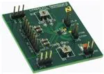
Demonstration Board Schematic
14
Submit Documentation Feedback
Copyright © 2008–2013, Texas Instruments Incorporated
Product Folder Links: LM48413
�LM48413
www.ti.com
SNAS460B – NOVEMBER 2008 – REVISED MARCH 2013
Demonstration Board Layout
Figure 20. Top Silkscreen
Submit Documentation Feedback
Copyright © 2008–2013, Texas Instruments Incorporated
Product Folder Links: LM48413
15
�LM48413
SNAS460B – NOVEMBER 2008 – REVISED MARCH 2013
www.ti.com
Figure 21. Top Layer
16
Submit Documentation Feedback
Copyright © 2008–2013, Texas Instruments Incorporated
Product Folder Links: LM48413
�LM48413
www.ti.com
SNAS460B – NOVEMBER 2008 – REVISED MARCH 2013
Figure 22. Middle Layer 1
Submit Documentation Feedback
Copyright © 2008–2013, Texas Instruments Incorporated
Product Folder Links: LM48413
17
�LM48413
SNAS460B – NOVEMBER 2008 – REVISED MARCH 2013
www.ti.com
Figure 23. Middle Layer 2
18
Submit Documentation Feedback
Copyright © 2008–2013, Texas Instruments Incorporated
Product Folder Links: LM48413
�LM48413
www.ti.com
SNAS460B – NOVEMBER 2008 – REVISED MARCH 2013
Figure 24. Bottom Layer
Revision Table
Rev
Date
1.0
11/19/08
Initial release.
Description
1.01
01/08/09
Text edits.
B
03/21/2013
Changed layout of National Data Sheet to TI format
Submit Documentation Feedback
Copyright © 2008–2013, Texas Instruments Incorporated
Product Folder Links: LM48413
19
�PACKAGE OPTION ADDENDUM
www.ti.com
10-Dec-2020
PACKAGING INFORMATION
Orderable Device
Status
(1)
Package Type Package Pins Package
Drawing
Qty
Eco Plan
(2)
Lead finish/
Ball material
MSL Peak Temp
Op Temp (°C)
Device Marking
(3)
(4/5)
(6)
LM48413TL/NOPB
ACTIVE
DSBGA
YZR
18
250
RoHS & Green
SNAGCU
Level-1-260C-UNLIM
-40 to 85
GL2
(1)
The marketing status values are defined as follows:
ACTIVE: Product device recommended for new designs.
LIFEBUY: TI has announced that the device will be discontinued, and a lifetime-buy period is in effect.
NRND: Not recommended for new designs. Device is in production to support existing customers, but TI does not recommend using this part in a new design.
PREVIEW: Device has been announced but is not in production. Samples may or may not be available.
OBSOLETE: TI has discontinued the production of the device.
(2)
RoHS: TI defines "RoHS" to mean semiconductor products that are compliant with the current EU RoHS requirements for all 10 RoHS substances, including the requirement that RoHS substance
do not exceed 0.1% by weight in homogeneous materials. Where designed to be soldered at high temperatures, "RoHS" products are suitable for use in specified lead-free processes. TI may
reference these types of products as "Pb-Free".
RoHS Exempt: TI defines "RoHS Exempt" to mean products that contain lead but are compliant with EU RoHS pursuant to a specific EU RoHS exemption.
Green: TI defines "Green" to mean the content of Chlorine (Cl) and Bromine (Br) based flame retardants meet JS709B low halogen requirements of