User's Guide
SNAA038A – May 2007 – Revised May 2013
AN-1589 LM48821 Evaluation Board
1
Quick Start Guide
1.
2.
3.
4.
5.
6.
7.
8.
2
Connect the I2C signal generation and interface board to a computer’s parallel port.
Install LM48821 control software: “LM48821_Software.”
Amplifier output mode:
Apply a 2.0V to 4.0V power supply’s positive voltage output to the “VDD” pin on jumper J6. Apply the
power supply’s ground return to the “GND“ pin on J6.
Connect the supplied 5-wire cable between the I2C signal generation and interface board and the 5-pin
connector (I2C Interface) on the LM48821 demonstration board.
Apply a stereo audio signal to jumpers JP2 (Left) and JP3 (Right). Apply the source’s +input and -input
to the “+” pin and the “-“ pin, respectively.
Connect a load (≥ 16Ω) to JP (Right) and another load to JP5 (Left). JP4’s “+” pin and JP’s “+” pin
carries the output signals from the two amplifiers found on pins OUTR and OUTL, respectively.
Apply power. Make measurements. Plug in a pair of headphones. Enjoy.
Introduction
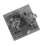
To help the user investigate and evaluate the LM48821's performance and capabilities, a fully populated
demonstration board is available from the Texas Instruments Audio Products Group. This board is shown
in Figure 1. Connected to an external power supply (2.0V to 4.0V), a signal source and an I2C controller
(or signal source), the LM48821 demonstration board easily demonstrate the amplifier's features.
All trademarks are the property of their respective owners.
SNAA038A – May 2007 – Revised May 2013
Submit Documentation Feedback
AN-1589 LM48821 Evaluation Board
Copyright © 2007–2013, Texas Instruments Incorporated
1
�General Description
www.ti.com
Figure 1. LM48821 Demonstration Board
3
General Description
The LM48821 is a fully differential input stereo headphone audio amplifier with an internal digitally
controlled volume control. The LM48821 is optimized to operate over a power supply voltage range of
2.0V to 4.0V. This amplifier is capable of delivering 53mWRMS per channel into a 32Ω load at 1% THD
when powered by a 3.0V power supply.
Boomer audio power amplifiers were designed specifically to provide high quality output power with a
minimal amount of external components. To that end, the LM48821 features two functions that optimize
system cost and minimize PCB area: an integrated, digitally controlled (I2C bus) volume control and an
amplifier generated negative power supply voltage that eliminates output signal-coupling capacitors. Since
the LM48821 does not require bootstrap capacitors, snubber networks, or output coupling capacitors, it is
optimally suited for low-power, battery powered potable systems.
The LM48821 includes separate shutdown controls for each stereo channel for micropower dissipation, an
internal thermal shutdown protection mechanism, and is unity gain stable.
4
Operating Conditions
•
•
5
Temperature Range –40°C ≤ TA ≤ 85°C
Amplifier Power Supply Voltage 2.0V ≤ VDD ≤ 5.0V ≤ 4.0V
Schematic
Figure 2 shows the LM48821 Demonstration Board schematic. Refer to Table 1 for a list of the
connections and their functions.
2
AN-1589 LM48821 Evaluation Board
SNAA038A – May 2007 – Revised May 2013
Submit Documentation Feedback
Copyright © 2007–2013, Texas Instruments Incorporated
�Board Features
INL-
1
SVDD
A4
+
1
PVDD
C1
J2
A1
D4
www.ti.com
2
0.47 PF
2
C2
A3
+
INL+
OUTL
B1
JU2
CUTHERE
1
2
0.47 PF
C4
B3
+
J3
J4
1
INR+
0.47 PF
2
C4
B4
U1
+
INR-
2
4
LM48821TL
0.47 PF
C2
5
3
SCL
SGND
J8
1
4
2
SCL
ADR
3
SDA
J1
I CVDD
2
GND
5
C3
SDA
OUTR
B2
3
C5
0.1 PF
C9
0.1 PF
C7
C8
4.7 PF
4.7 PF
SGND
J5
2
A2
PGND
D2
VSS
C1
CPP
CPM
D1
2
1
C6
4.7 PF
1
2
I CVDD
D3
C4
2
JU1
J6
1
Figure 2. LM48821 Demonstration Board Schematic
6
Board Features
The LM48821 demonstration board has all of the necessary connections, using 0.100” headers, to apply
the power supply voltage, the audio input signals, and the I2C signal inputs. The amplified audio signal is
available on both a stereo headphone jack and auxiliary output connections.
Also included with the demonstration board is an I2C signal generation board and software. With this
board and the software, the user can easily control the LM48821’s, shutdown function, mute, and stereo
volume control. Figure 3 shows the software’s graphical user interface.
Figure 3. LM48821 Software User's Interface
SNAA038A – May 2007 – Revised May 2013
Submit Documentation Feedback
AN-1589 LM48821 Evaluation Board
Copyright © 2007–2013, Texas Instruments Incorporated
3
�Connections
7
www.ti.com
Connections
Connecting to the world is accomplished through the 0.100” headers on the LM48821 demonstration
board. The functions of the different headers are detailed in Table 1.
Table 1. LM48821 Demonstration Board Connections
Jumper Designation
Function or Use
J1
Stereo, 0.125” headphone jack. Left channel is on the tip connector and the right channel is on
the ring connector. Ground is on the sleeve connector.
J2
This is the connection to the amplifier’s differential left channel input. Apply an external
differential signal source’s positive voltage to the J2 pin labeled “L IN+” and the signal source’s
negative input to the pin labeled “L IN-.”
J3
This is the connection to the amplifier’s differential right channel input. Apply an external
differential signal source’s positive voltage to the J3 pin labeled “R IN+” and the signal source’s
negative input to the pin labeled “R IN-.”
J4
This is the connection to the amplifier’s single-ended, ground- referenced right channel output.
Connect the J4 pin labeled “R OUT+” and the pin labeled “R OUT-” to the positive and ground
inputs, respectively, of an external signal measurement device. J4’s pin labeled “R OUT+”
corresponds to the headphone jack’s “ring” connection. J4’s pin labeled “R OUT-“ corresponds
to the headphone jack’s “sleeve” (or ground) connection.
J5
This is the connection to the amplifier’s single-ended, ground- referenced left channel output.
Connect the J5 pin labeled “L OUT+” and the pin labeled “L OUT-” to the positive and ground
inputs, respectively, of an external signal measurement device. J5’s pin labeled “L OUT+”
corresponds to the headphone jack’s “tip” connection. J5’s pin labeled “L OUT-“ corresponds to
the headphone jack’s “sleeve” (or ground) connection.
J6
Power supply connection. Connect an external power supply’s positive voltage source (2.0V to
4.0V) to the J6 pin labeled “VDD” and the supply’s ground source to the pin labeled “GND.”
J8 (I2C Interface)
JU1
8
This is the input connection for the I2C serial clock and serial data signals. J8-pin 1 is for the
SCL signal, JP8-pin 2 is not used. J8-pin 3 is for the SDA signal. J8-pin 4 is for an I2C VDD
supply voltage supplied by the I2C signal source. J8-pin 5 is for ground.
If an external I2C power supply voltage is used, connect this supply’s positive voltage source to
the JU1 pin labeled “I2CVDD” and the supply’s ground source to the pin labeled “GND.” If the
external VDD power supply is used for the I2CVDDvoltage, place a jumper between the JU1 pin
labeled “VDD” and the JU1 pin labeled “I2CVDD.”
Power Supply Sequencing
The LM48821 uses two power supply voltages: VDD for the analog circuitry and I2CVDD, which defines the
digital control logic high voltage level. To ensure proper functionality, apply VDD first, followed by I2CVDD. If
one power supply is used, VDD and I2CVDD can be connected together. The part will power-up with both
channels shutdown, the volume control set to minimum, and the mute function active.
9
I2C Signal Generation Board and Software
The I2C signal generation and interface board, along with the LM48821 software, will generate the address
byte and the data byte used in the I2C control data transaction. To use the I2C signal generation and
interface board, please plug it into a PC’s parallel port (on either a notebook or a desktop computer).
The software comes with an installer. To install, unzip the file titled “LM48821_Software.” After the file
unzips, double-click the “setup.exe” file. After it launches, please follow the installer’s instructions. Setup
will create a folder named “LM48821” in the “Program” folder on the “C” disk (if the default is used) along
with a shortcut of the same name in the “Programs” folder in the “Start” menu.
The LM48821 program includes controls for the amplifier’s volume control, individual channel shutdown,
and the mute function. The control program's on-screen user interface is shown in Figure 3.
The Default button is used to return the LM48821 to its power-on reset state: minimum volume setting,
shutdown on both amplifiers active, and mute active.
The LM48821’s stereo VOLUME CONTROL has 32 steps and a gain range of –76dB to 18dB. It is
controlled using the slider located at the bottom of the program’s window. Each time the slider is moved
from one tick mark to another, the program updates the amplifier’s volume control.
4
AN-1589 LM48821 Evaluation Board
SNAA038A – May 2007 – Revised May 2013
Submit Documentation Feedback
Copyright © 2007–2013, Texas Instruments Incorporated
�PCB Layout Guidelines
www.ti.com
LEFT CHANNEL, BOTH CHANNELS, and RIGHT CHANNEL controls each have two buttons. For the
left and right channel control, the “ON” button activates its respective channel, whereas the “OFF” button
places its respective channel in shutdown mode. Selecting the BOTH CHANNELS “ON” button
simultaneously activates both channels, whereas selecting the “OFF” button places channels in shutdown
mode.
10
PCB Layout Guidelines
This section provides general practical guidelines for PCB layouts that use various power and ground
traces. Designers should note that these are only "rule-of-thumb" recommendations and the actual results
are predicated on the final layout.
10.1 Power and Ground Circuits
Star trace routing techniques (returning individual traces back to a central point rather than daisy chaining
traces together in a serial manner) can have a major positive impact on low-level signal performance. Star
trace routing refers to using individual traces that radiate from a signal point to feed power and ground to
each circuit or even device. This technique may require greater design time, but should not increase the
final price of the board.
For good THD + N and low noise performance and to ensure correct power-on behavior at the maximum
allowed supply voltage, a local 4.7μF power supply bypass capacitor should be connected as physically
close as possible to the PVDD pin.
10.2 Avoiding Typical Design/Layout Problems
Avoid ground loops or running digital and analog traces parallel to each other (side-by-side) on the same
PCB layer. When traces must cross over each other, do so at 90 degrees. Running digital and analog
traces at 90 degrees to each other from the top to the bottom side as much as possible will minimize
capacitive noise coupling and crosstalk.
11
Bill of Materials
Designator
Part Description
Value
Tolerance
Rating
Package
Type
Manufacturer
Manufacturer's Part
Number
C1–C4
TACmicrochip
tantalum capacitor
0.47μF
±20%
10V
0402
AVX
TACK474M010PTA
C5, C9
Multilayer Ceramic
Capacitor
0.1μF
±10%
6.3V
0201
TDK
C0603X5R1A104M
C6, C8
Multilayer Ceramic
Capacitor
4.7μF
±20%
6.3V
0603
TDK
C1608X5R1A475M
C7
Multilayer Ceramic
Capacitor
4.7μF
±20%
10V
0805
TDK
C2012X5R1A475M
J1
Headphone Jack
J2–J6
2-pin header, 100mil
lead pitch
J8
5-pin header, 100mil
lead pitch
JU1
3-pin header, 100mil
lead pitch
U1
LM48821Direct
Coupled Tru-GND,
Ultra Low Noise,
80mW Differential
Inputs Stereo
Headphone Amplifier
with I2C Volume
Control
Texas
Instruments
SNAA038A – May 2007 – Revised May 2013
Submit Documentation Feedback
LM48821
AN-1589 LM48821 Evaluation Board
Copyright © 2007–2013, Texas Instruments Incorporated
5
�Demonstration Board PCB Layout
12
www.ti.com
Demonstration Board PCB Layout
Figure 4 through Figure 9 show the different layers used to create the LM48821 four-layer demonstration
board. Figure 4 is the silkscreen that shows parts location, Figure 5 is the top layer, Figure 6 is the upper
middle layer, Figure 7 is the lower middle layer, Figure 8 is the bottom layer, and Figure 9 is the bottom
silkscreen layer.
Figure 4. Top Silkscreen (Shown 2.6X actual size)
Figure 5. Top Layer (Shown 2.6X actual size)
Figure 6. Upper Middle Layer (Shown 2.6X actual size)
6
AN-1589 LM48821 Evaluation Board
SNAA038A – May 2007 – Revised May 2013
Submit Documentation Feedback
Copyright © 2007–2013, Texas Instruments Incorporated
�Demonstration Board PCB Layout
www.ti.com
Figure 7. Lower Middle Layer (Shown 2.6X actual size)
Figure 8. Bottom Layer (Shown 2.6X actual size)
Figure 9. Bottom Silk Layer (Shown 2.6X actual size)
SNAA038A – May 2007 – Revised May 2013
Submit Documentation Feedback
AN-1589 LM48821 Evaluation Board
Copyright © 2007–2013, Texas Instruments Incorporated
7
�Typical Performance
13
www.ti.com
Typical Performance
10
10
5
5
1
THD+N (%)
THD+N (%)
1
0.5
0.1
0.05
0.1
0.05
0.01
0.005
30u 100u
0.5
0.01
1m
10m 100m
0.005
30u 100u
300m
OUTPUT POWER (W)
Figure 10. Stereo THD+N vs Output Power
RL = 16Ω, AV = 0dB, f = 100Hz
at (from left to right at 1% THD+N):
VDD = 2V, VDD = 3V, VDD = 4V,
both channels driven and measured
10
5
5
300m
1
THD+N (%)
THD+N (%)
1
0.5
0.1
0.05
0.5
0.1
0.05
0.01
0.01
1m
10m 100m
300m
0.005
30u 100u
OUTPUT POWER (W)
Figure 12. Stereo THD+N vs Output Power
RL = 16Ω, AV = 0dB, f = 10kHz
at (from left to right at 1% THD+N):
VDD = 2V, VDD = 3V, VDD = 4V,
both channels driven and measured
8
10m 100m
Figure 11. Stereo THD+N vs Output Power
RL = 16Ω, AV = 0dB, f = 1kHz
at (from left to right at 1% THD+N):
VDD = 2V, VDD = 3V, VDD = 4V,
both channels driven and measured
10
0.005
30u 100u
1m
OUTPUT POWER (W)
1m
10m 100m
300m
OUTPUT POWER (W)
Figure 13. Stereo THD+N vs Output Power
RL = 32Ω, AV = 0dB, f = 100Hz
at (from left to right at 1% THD+N):
VDD = 2V, VDD = 3V, VDD = 4V,
both channels driven and measured
AN-1589 LM48821 Evaluation Board
SNAA038A – May 2007 – Revised May 2013
Submit Documentation Feedback
Copyright © 2007–2013, Texas Instruments Incorporated
�Typical Performance
www.ti.com
10
10
5
5
1
THD+N (%)
THD+N (%)
1
0.5
0.1
0.05
0.1
0.05
0.01
0.005
30u 100u
0.5
0.01
1m
10m 100m
0.005
30u 100u
300m
OUTPUT POWER (W)
10m 100m
300m
Figure 15. Stereo THD+N vs Output Power
RL = 32Ω, AV = 0dB, f = 10kHz
at (from left to right at 1% THD+N):
VDD = 2V, VDD = 3V, VDD = 4V,
both channels driven and measured
0.5
0.5
0.1
0.1
THD+N (%)
THD+N (%)
Figure 14. Stereo THD+N vs Output Power
RL = 32Ω, AV = 0dB, f = 1kHz
at (from left to right at 1% THD+N):
VDD = 2V, VDD = 3V, VDD = 4V,
both channels driven and measured
0.05
0.01
0.005
20
1m
OUTPUT POWER (W)
0.05
0.01
100 200
1k 2k
10k 20k
0.005
20
FREQUENCY (Hz)
Figure 16. Stereo THD+N vs Frequency
RL = 16Ω, AV = 0dB
at (from left to bottom at 10kHz):
VDD = 2V, POUT = 7mW;
VDD = 3V, POUT = 36mW;
VDD = 4V, POUT = 92mW;
both channels driven and measured
100 200
1k 2k
10k 20k
FREQUENCY (Hz)
Figure 17. Stereo THD+N vs Frequency
RL = 32Ω, AV = 0dB
at (from left to bottom at 10kHz):
VDD = 2V, POUT = 10mW;
VDD = 3V, POUT = 38mW;
VDD = 4V, POUT = 85mW;
both channels driven and measured
SNAA038A – May 2007 – Revised May 2013
Submit Documentation Feedback
AN-1589 LM48821 Evaluation Board
Copyright © 2007–2013, Texas Instruments Incorporated
9
�www.ti.com
Appendix A LM48821 I2C Control Register
Table 2 shows the actions that are implemented by manipulating the bits within the internal I2C control
register.
Table 2. LM48821 I2C Control Register Addressing and Data Format Chart
I2C Address
Control
Register
D7
D6
D5
D4
D3
D2
D1
1
1
1
0
1
1
0
D0
0
V4
V3
V2
V1
V0
MUTE
LEFT
ENABLE
RIGHT
ENABLE
Appendix B Volume Control Settings Binary Values
The minimum volume setting is set to –76dB when 00000 is loaded into the volume control register.
Incrementing the volume control register in binary fashion increases the volume control setting, reaching
full scale at 11111. Table 3 shows the value of the gain for each of the 32 binary volume control settings.
Table 3. Binary Values for the Different Volume Control Gain Settings
10
Gain
B4
B3
B2
B1
B0
18
1
1
1
1
1
17
1
1
1
1
0
16
1
1
1
0
1
15
1
1
1
0
0
14
1
1
0
1
1
13
1
1
0
1
0
12
1
1
0
0
1
10
1
1
0
0
0
8
1
0
1
1
1
6
1
0
1
1
0
4
1
0
1
0
1
2
1
0
1
0
0
0
1
0
0
1
1
–2
1
0
0
1
0
–4
1
0
0
0
1
–6
1
0
0
0
0
–8
0
1
1
1
1
–10
0
1
1
1
0
–12
0
1
1
0
1
–14
0
1
1
0
0
–16
0
1
0
1
1
–18
0
1
0
1
0
–21
0
1
0
0
1
–24
0
1
0
0
0
–27
0
0
1
1
1
–30
0
0
1
1
0
–34
0
0
1
0
1
–38
0
0
1
0
0
–44
0
0
0
1
1
–52
0
0
0
1
0
–62
0
0
0
0
1
LM48821 I2C Control Register
SNAA038A – May 2007 – Revised May 2013
Submit Documentation Feedback
Copyright © 2007–2013, Texas Instruments Incorporated
�Appendix C
www.ti.com
Table 3. Binary Values for the Different Volume Control Gain Settings (continued)
Gain
B4
B3
B2
B1
B0
–76
0
0
0
0
0
Appendix C Micro SMD Wafer Level Chip Scale Package, PCB, Layout, and Mounting
Considerations
Please refer to AN-1112 DSBGA Wafer Level Chip Scale Package (SNVA009) for possible updates to the
μSMD package information.
Appendix D Revision History
Rev
Date
Description
1.0
05/14/07
Initial release.
SNAA038A – May 2007 – Revised May 2013
Submit Documentation Feedback
Micro SMD Wafer Level Chip Scale Package, PCB, Layout, and Mounting
Considerations
Copyright © 2007–2013, Texas Instruments Incorporated
11
�IMPORTANT NOTICE
Texas Instruments Incorporated and its subsidiaries (TI) reserve the right to make corrections, enhancements, improvements and other
changes to its semiconductor products and services per JESD46, latest issue, and to discontinue any product or service per JESD48, latest
issue. Buyers should obtain the latest relevant information before placing orders and should verify that such information is current and
complete. All semiconductor products (also referred to herein as “components”) are sold subject to TI’s terms and conditions of sale
supplied at the time of order acknowledgment.
TI warrants performance of its components to the specifications applicable at the time of sale, in accordance with the warranty in TI’s terms
and conditions of sale of semiconductor products. Testing and other quality control techniques are used to the extent TI deems necessary
to support this warranty. Except where mandated by applicable law, testing of all parameters of each component is not necessarily
performed.
TI assumes no liability for applications assistance or the design of Buyers’ products. Buyers are responsible for their products and
applications using TI components. To minimize the risks associated with Buyers’ products and applications, Buyers should provide
adequate design and operating safeguards.
TI does not warrant or represent that any license, either express or implied, is granted under any patent right, copyright, mask work right, or
other intellectual property right relating to any combination, machine, or process in which TI components or services are used. Information
published by TI regarding third-party products or services does not constitute a license to use such products or services or a warranty or
endorsement thereof. Use of such information may require a license from a third party under the patents or other intellectual property of the
third party, or a license from TI under the patents or other intellectual property of TI.
Reproduction of significant portions of TI information in TI data books or data sheets is permissible only if reproduction is without alteration
and is accompanied by all associated warranties, conditions, limitations, and notices. TI is not responsible or liable for such altered
documentation. Information of third parties may be subject to additional restrictions.
Resale of TI components or services with statements different from or beyond the parameters stated by TI for that component or service
voids all express and any implied warranties for the associated TI component or service and is an unfair and deceptive business practice.
TI is not responsible or liable for any such statements.
Buyer acknowledges and agrees that it is solely responsible for compliance with all legal, regulatory and safety-related requirements
concerning its products, and any use of TI components in its applications, notwithstanding any applications-related information or support
that may be provided by TI. Buyer represents and agrees that it has all the necessary expertise to create and implement safeguards which
anticipate dangerous consequences of failures, monitor failures and their consequences, lessen the likelihood of failures that might cause
harm and take appropriate remedial actions. Buyer will fully indemnify TI and its representatives against any damages arising out of the use
of any TI components in safety-critical applications.
In some cases, TI components may be promoted specifically to facilitate safety-related applications. With such components, TI’s goal is to
help enable customers to design and create their own end-product solutions that meet applicable functional safety standards and
requirements. Nonetheless, such components are subject to these terms.
No TI components are authorized for use in FDA Class III (or similar life-critical medical equipment) unless authorized officers of the parties
have executed a special agreement specifically governing such use.
Only those TI components which TI has specifically designated as military grade or “enhanced plastic” are designed and intended for use in
military/aerospace applications or environments. Buyer acknowledges and agrees that any military or aerospace use of TI components
which have not been so designated is solely at the Buyer's risk, and that Buyer is solely responsible for compliance with all legal and
regulatory requirements in connection with such use.
TI has specifically designated certain components as meeting ISO/TS16949 requirements, mainly for automotive use. In any case of use of
non-designated products, TI will not be responsible for any failure to meet ISO/TS16949.
Products
Applications
Audio
www.ti.com/audio
Automotive and Transportation
www.ti.com/automotive
Amplifiers
amplifier.ti.com
Communications and Telecom
www.ti.com/communications
Data Converters
dataconverter.ti.com
Computers and Peripherals
www.ti.com/computers
DLP® Products
www.dlp.com
Consumer Electronics
www.ti.com/consumer-apps
DSP
dsp.ti.com
Energy and Lighting
www.ti.com/energy
Clocks and Timers
www.ti.com/clocks
Industrial
www.ti.com/industrial
Interface
interface.ti.com
Medical
www.ti.com/medical
Logic
logic.ti.com
Security
www.ti.com/security
Power Mgmt
power.ti.com
Space, Avionics and Defense
www.ti.com/space-avionics-defense
Microcontrollers
microcontroller.ti.com
Video and Imaging
www.ti.com/video
RFID
www.ti-rfid.com
OMAP Applications Processors
www.ti.com/omap
TI E2E Community
e2e.ti.com
Wireless Connectivity
www.ti.com/wirelessconnectivity
Mailing Address: Texas Instruments, Post Office Box 655303, Dallas, Texas 75265
Copyright © 2013, Texas Instruments Incorporated
�