User's Guide
SNVA393B – March 2009 – Revised April 2013
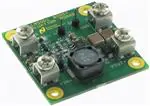
AN-1956 LM5001 Boost Evaluation Board
1
Introduction
The LM5001 boost evaluation board is designed to provide the design engineer with a fully functional
power converter based on the boost topology to evaluate the LM5001 high voltage switch mode regulator.
The performance of the evaluation board is as follows:
Input Operating Range: 16 to 36V
Output Voltage: 48V
Output Current: 0 to 150 mA
Measured Efficiency: 91% @ 150 mA, 86% @ 75 mA
Frequency of Operation: 240 kHz
Board Size: 1.75 X 1.75 inches
Load Regulation: 1%
Line Regulation: 0.1%
The printed circuit board consists of 2 layers; 1 ounce copper layers FR4 material with a total thickness of
0.062 inches.
When laying out the PCB note the proximity of the ground pin (pin 4) to the output capacitors (see the
schematic in Section 2). Placing the ground pin near the output capacitor will minimize the ripple in the
output by forcing a constant current to flow across the board for both the switch on and switch off portions
of the cycle. If the board is laid out with the ground pin near the input capacitor then a high di/dt condition
will occur due to the small conduction loop area during the switch on time and large loop conduction area
during the switch off time. The output ripple and noise will be minimized if the conduction loop area and
current both remain constant. Placing the ground pin near the output capacitor accomplishes this goal.
All trademarks are the property of their respective owners.
SNVA393B – March 2009 – Revised April 2013
Submit Documentation Feedback
AN-1956 LM5001 Boost Evaluation Board
Copyright © 2009–2013, Texas Instruments Incorporated
1
�Schematic
2
www.ti.com
Schematic
6.8 R6
L1
C8
470 pF
D2
J1
J3
16V to 36V IN
C1
2.2 PF
100 PH
C2
2.2 PF
CMSH2-60M
C11
4.7 PF
C9
4.7 PF
C10
1 PF
+48V, 150 mA
J2
J4
R1
100k
GND
J7
GND
R2
10.0
GND
R8
0
J5
C3
0.1 PF
ENABLE
U1
2
8
5
R3
9.09k
4
C4
0.01 PF
VIN
EN
VCC
SW
RT
COMP
GND
FB
C12
3
22 pF
1
R7 73.2k
7
C13
6
2200 pF
LM5001M
D1
R9
54.9k
BAT54S
R10
1.47k
J6
SYNC
R5
100k
C5
100 pF
R4
53.6k
C6
1 PF
C7
10 PF
Softstart
2
AN-1956 LM5001 Boost Evaluation Board
Copyright © 2009–2013, Texas Instruments Incorporated
SNVA393B – March 2009 – Revised April 2013
Submit Documentation Feedback
�Powering and Loading Considerations
www.ti.com
3
Powering and Loading Considerations
When applying power to the LM5001 Boost evaluation board certain precautions need to be followed. A
misconnection can damage the board.
3.1
Proper Connections
When operated at low input voltages the evaluation board can draw up to 500mA of current at full load.
The maximum rated output current is 150mA. Be sure to choose the correct connector and wire size when
attaching the source supply and the load. Monitor the current into and out of the evaluation board. Monitor
the voltage directly at the output terminals of the evaluation board. The voltage drop across the load
connecting wires will give inaccurate measurements. This is especially true for accurate efficiency
measurements. When measuring output ripple with an oscilloscope. Do not use the wire ground lead for
the ground connection. The loop formed by the wire lead will pick up noise from the switching circuits and
make the ripple voltage look larger then it actually is. Instead use a spring ground clip on the exposed
ground ring on the scope probe to minimize the loop area of the ground lead. An alternative is to remove
the shroud covering the scope probe. Then touch the exposed scope probe ground connection to the
output ground terminal while simultaneously connecting the probe tip to the output terminal.
3.2
Source Power
The power supply and cabling must look like a low impedance voltage source to the evaluation board.
High inductance power supply leads like the type typically used for bench power supplies, could cause the
LM5001 to become unstable or have poor response to load transients. This is due to the inductance of the
power supply wiring interacting with the evaluation board input capacitor and causing a series resonant LC
oscillation at a frequency defined by the inductance of the input wiring and the value of the input capacitor.
In some cases it may be necessary to add an additional capacitor in parallel with input capacitor to move
the resonate frequency away from the unity gain crossover frequency of the LM5001. Twisting the input
supply lines together will reduce the inductance and potential for problems. Powering up at max rated
voltage or close to this voltage can cause damage due to the inductance of the supply lines. Over shoot
and ringing can be several volts under a sudden application of power. When operating near maximum
input voltage slowly ramp up the voltage to avoid overshoot.
3.3
Loading
An appropriate electronic load, with specified operation up to 48V maximum or more, is desirable. Monitor
both current and voltage at all times. Ensure there is sufficient cooling provided for the load.
3.4
Over Current Protection
The LM5001 monitors the peak current through the inductor on a cycle by cycle basis. If the inductor is
sized large enough to not saturate when operating at peak current limit. Then the short circuit can be left
on indefinitely with out damaging the device or causing it to go into thermal shutdown.
Scope
36 Volt, 1 AmpPower Supply
with Current
Meter
+
Volt-meter
-
Volt-meter
Evaluation Board
Current-meter
IN
+
+
ON/OFF
(SHUTDOWN)
OUT
-
-
+
10 Watt, 1 Amp
Electronic Load
Jumper
Figure 1. Typical Evaluation Setup
SNVA393B – March 2009 – Revised April 2013
Submit Documentation Feedback
AN-1956 LM5001 Boost Evaluation Board
Copyright © 2009–2013, Texas Instruments Incorporated
3
�Performance Characteristics
4
www.ti.com
Performance Characteristics
Turn-on Waveforms
Figure 2 shows the output voltage during a typical start-up with a 20V input and a load of 150 mA. There
is no overshoot during startup.
Output Ripple Waveforms
Figure 3 shows the transient response for a load of change from 15 mA to 150 mA. The upper trace
shows minimal output voltage droop and overshoot during the sudden change in output current shown by
the lower trace.
Conditions:
Input Voltage = 20VDC
Output Current = 150 mA
Trace 1:
Output Voltage
Volts/div = 10V
Horizontal Resolution = 4.0 ms/div
Figure 2. Output Voltage During a Typical Start-Up With a 20V Input and a Load of 150 mA
Conditions:
Input Voltage = 20VDC
Output Current = 15 mA to 150 mA
Upper Trace:
Output Voltage
Volts/div = 500 mV
Lower Trace:
Output Current
150 mA to 15 mA to 150 mA
Horizontal Resolution = 0.4 ms/div
Figure 3. Transient Response for a Load of Change From 15 mA to 150 mA
4
AN-1956 LM5001 Boost Evaluation Board
Copyright © 2009–2013, Texas Instruments Incorporated
SNVA393B – March 2009 – Revised April 2013
Submit Documentation Feedback
�Performance Characteristics
www.ti.com
Conditions:
Input Voltage = 20VDC
Output Current = 150 mA
Bandwidth Limit = 20 MHz
Trace 1:
Output Voltage
Volts/div = 20 mV
Horizontal Resolution = 1 µs/div
Figure 4. Typical Output Ripple for an Input Voltage of 20V and a Load of 150 mA
Figure 4 shows typical output ripple, seen directly across the output capacitor, for an input voltage of 20V
and a load of 150 mA. This waveform is typical of most loads and input voltages.
Figure 5 shows power efficiency over full input voltage and output current range. Peak efficiency is at full
rated load and is greater then 90% across the input voltage range.
Figure 6 shows the small signal closed loop response with 20V input and 150 mA load current into a
resistive load. The gain curve starts at around 60dB the phase curve starts at around 45°. 0dB of
crossover frequency is at 11 kHz with a phase margin of 70°.
Conditions:
Input Voltage = 16 - 36VDC
Output Current = 10 mA - 150 mA
Figure 5. Power Efficiency Over Full Input Voltage and Output Current Range
SNVA393B – March 2009 – Revised April 2013
Submit Documentation Feedback
AN-1956 LM5001 Boost Evaluation Board
Copyright © 2009–2013, Texas Instruments Incorporated
5
�Performance Characteristics
www.ti.com
Conditions:
Input Voltage = 20VDC
Output Current = 150 mA
Figure 6. Small Signal Closed Loop Response With 20V Input and 150 mA Load
6
AN-1956 LM5001 Boost Evaluation Board
Copyright © 2009–2013, Texas Instruments Incorporated
SNVA393B – March 2009 – Revised April 2013
Submit Documentation Feedback
�Bill of Materials
www.ti.com
5
Bill of Materials
Table 1. Bill of Materials
Designator
Qty
Part Number
Description
Value
C1, C2
2
GRM31CR71H225KA88L
CAPACITOR, 1206 X7R CER, Murata
2.2µF, 50V
C3
1
C2012X7R1H104M
CAPACITOR, 0805 X7R CER, TDK
0.1µF, 50V
C4
1
C2012X7R1H103M
CAPACITOR, 0805 X7R CER, TDK
0.01µF, 50V
C5
1
C2012COG1H101J
CAPACITOR, 0805 COG CER, TDK
100pF, 50V
C6
1
C3216X7R1C105K
CAPACITOR, 0805 X7R CER, TDK
1µF, 16V
C7
1
GRM21BR61C106KE15L
CAPACITOR, 0805 X7R CER, Murata
10µF, 16V
C8
1
C2012COG1H471J
CAPACITOR, 0805 COG CER, TDK
470pF, 100V
C9, C11
2
C5750X7R2A475M
CAPACITOR, 2220 X7R CER, TDK
4.7µF, 100V
C10
1
C3225X7R2A105K
CAPACITOR, 1210 X7R CER, TDK
1µF, 100V
C12
1
C2012COG1H220J
CAPACITOR, 0805 COG CER, TDK
22pF, 50V
C13
1
C2012COG1H222J
CAPACITOR, 0805 COG CER, TDK
2200pF, 50V
D1
1
BAT54S
DIODE, SOT-23, DUAL, SCHOTTKY, Fairchild
Semiconductor
200mA, 30V
CMSH2-60M
DIODE, SMA, SCHOTTKY, Central
Semiconductor Corp.
2A, 60V
MSS1260
INDUCTOR, COILCRAFT
100µH, 1.8A
100K
D2
L1
1
R1, R5
2
CRCW08051003F
RESISTOR, 0805, VISHAY
R2
1
CRCW080510R0F
RESISTOR, 0805, VISHAY
10
R3
1
CRCW08059091F
RESISTOR, 0805, VISHAY
9.09K
R4
1
CRCW08055362F
RESISTOR, 0805, VISHAY
53.6K
R6
1
CRCW080568R1F
RESISTOR, 0805, VISHAY
6.8
R7
1
CRCW08057322F
RESISTOR, 0805, VISHAY
73.2K
R8
1
CRCW08050000F
RESISTOR, 0805, VISHAY
0
R9
1
CRCW08055492F
RESISTOR, 0805, VISHAY
54.9K
1.47K
CRCW08051471F
RESISTOR, 0805, VISHAY
J1, J2, J3, J4
R10
4
7693
Keystone Screw Terminal
J5, J6, J7
Mar-36
PTC36SAAN
0.025" Sq post, 36 position, Sullins
LM5001
High Voltage Switch Mode Regulator, Texas
Instruments
U1
1
SNVA393B – March 2009 – Revised April 2013
Submit Documentation Feedback
3 posts used
AN-1956 LM5001 Boost Evaluation Board
Copyright © 2009–2013, Texas Instruments Incorporated
7
�Printed Circuit Layout
6
www.ti.com
Printed Circuit Layout
Figure 7. Silkscreen Layer
Figure 8. Top Layer
8
AN-1956 LM5001 Boost Evaluation Board
Copyright © 2009–2013, Texas Instruments Incorporated
SNVA393B – March 2009 – Revised April 2013
Submit Documentation Feedback
�Printed Circuit Layout
www.ti.com
Figure 9. Bottom Layer
SNVA393B – March 2009 – Revised April 2013
Submit Documentation Feedback
AN-1956 LM5001 Boost Evaluation Board
Copyright © 2009–2013, Texas Instruments Incorporated
9
�IMPORTANT NOTICE
Texas Instruments Incorporated and its subsidiaries (TI) reserve the right to make corrections, enhancements, improvements and other
changes to its semiconductor products and services per JESD46, latest issue, and to discontinue any product or service per JESD48, latest
issue. Buyers should obtain the latest relevant information before placing orders and should verify that such information is current and
complete. All semiconductor products (also referred to herein as “components”) are sold subject to TI’s terms and conditions of sale
supplied at the time of order acknowledgment.
TI warrants performance of its components to the specifications applicable at the time of sale, in accordance with the warranty in TI’s terms
and conditions of sale of semiconductor products. Testing and other quality control techniques are used to the extent TI deems necessary
to support this warranty. Except where mandated by applicable law, testing of all parameters of each component is not necessarily
performed.
TI assumes no liability for applications assistance or the design of Buyers’ products. Buyers are responsible for their products and
applications using TI components. To minimize the risks associated with Buyers’ products and applications, Buyers should provide
adequate design and operating safeguards.
TI does not warrant or represent that any license, either express or implied, is granted under any patent right, copyright, mask work right, or
other intellectual property right relating to any combination, machine, or process in which TI components or services are used. Information
published by TI regarding third-party products or services does not constitute a license to use such products or services or a warranty or
endorsement thereof. Use of such information may require a license from a third party under the patents or other intellectual property of the
third party, or a license from TI under the patents or other intellectual property of TI.
Reproduction of significant portions of TI information in TI data books or data sheets is permissible only if reproduction is without alteration
and is accompanied by all associated warranties, conditions, limitations, and notices. TI is not responsible or liable for such altered
documentation. Information of third parties may be subject to additional restrictions.
Resale of TI components or services with statements different from or beyond the parameters stated by TI for that component or service
voids all express and any implied warranties for the associated TI component or service and is an unfair and deceptive business practice.
TI is not responsible or liable for any such statements.
Buyer acknowledges and agrees that it is solely responsible for compliance with all legal, regulatory and safety-related requirements
concerning its products, and any use of TI components in its applications, notwithstanding any applications-related information or support
that may be provided by TI. Buyer represents and agrees that it has all the necessary expertise to create and implement safeguards which
anticipate dangerous consequences of failures, monitor failures and their consequences, lessen the likelihood of failures that might cause
harm and take appropriate remedial actions. Buyer will fully indemnify TI and its representatives against any damages arising out of the use
of any TI components in safety-critical applications.
In some cases, TI components may be promoted specifically to facilitate safety-related applications. With such components, TI’s goal is to
help enable customers to design and create their own end-product solutions that meet applicable functional safety standards and
requirements. Nonetheless, such components are subject to these terms.
No TI components are authorized for use in FDA Class III (or similar life-critical medical equipment) unless authorized officers of the parties
have executed a special agreement specifically governing such use.
Only those TI components which TI has specifically designated as military grade or “enhanced plastic” are designed and intended for use in
military/aerospace applications or environments. Buyer acknowledges and agrees that any military or aerospace use of TI components
which have not been so designated is solely at the Buyer's risk, and that Buyer is solely responsible for compliance with all legal and
regulatory requirements in connection with such use.
TI has specifically designated certain components as meeting ISO/TS16949 requirements, mainly for automotive use. In any case of use of
non-designated products, TI will not be responsible for any failure to meet ISO/TS16949.
Products
Applications
Audio
www.ti.com/audio
Automotive and Transportation
www.ti.com/automotive
Amplifiers
amplifier.ti.com
Communications and Telecom
www.ti.com/communications
Data Converters
dataconverter.ti.com
Computers and Peripherals
www.ti.com/computers
DLP® Products
www.dlp.com
Consumer Electronics
www.ti.com/consumer-apps
DSP
dsp.ti.com
Energy and Lighting
www.ti.com/energy
Clocks and Timers
www.ti.com/clocks
Industrial
www.ti.com/industrial
Interface
interface.ti.com
Medical
www.ti.com/medical
Logic
logic.ti.com
Security
www.ti.com/security
Power Mgmt
power.ti.com
Space, Avionics and Defense
www.ti.com/space-avionics-defense
Microcontrollers
microcontroller.ti.com
Video and Imaging
www.ti.com/video
RFID
www.ti-rfid.com
OMAP Applications Processors
www.ti.com/omap
TI E2E Community
e2e.ti.com
Wireless Connectivity
www.ti.com/wirelessconnectivity
Mailing Address: Texas Instruments, Post Office Box 655303, Dallas, Texas 75265
Copyright © 2013, Texas Instruments Incorporated
�