User's Guide
SNVA292A – October 2007 – Revised April 2013
AN-1725 LM5015 Non-Isolated Two-Switch DC-DC
Regulator Evaluation Board
1
Introduction
The LM5015 Non-Isolated DC-DC Regulator evaluation board provides a low cost and fully functional DCDC regulator without employing any discrete power MOSFET. The evaluation board can be configured as
either a Non-Isolated Two-Switch Forward DC-DC Regulator, or a Two-Switch Flyback DC-DC Regulator.
The factory default configuration of the evaluation board is Forward topology. The former configuration will
produce about 2% higher efficiency and lower output ripple voltage than the flyback. Whereas, the Flyback
configuration costs slightly less. Suggestion to reconfigure the evaluation board as an Non-Isolated TwoSwitch Flyback DC-DC Regulator is provided at the end of this article.
For detailed features and technical information of the LM5015 device, see the LM5015 High Voltage
Monolithic Two-Switch Forward DC-DC Regulator Data Sheet (SNVS538). For isolated applications, see
the AN-1724 LM5015 Isolated Two-Switch DC-DC Regulator Evaluation Board User's Guide (SNVA291).
The evaluation board features:
• Input Voltage: 36V to 72V
• Output Voltage: 5V
• Output Current: 0A minimum, 2.5A nominal, and 3A maximum
• Input UVLO Threshold: 34V nominal
• Measured Efficiency: 86% (VIN = 48V, IOUT = 2.5A)
• Switching Frequency: 300 kHz
• Ability to Synchronize to External Clock
• Ability to Be Remote Controlled (Enable/Disable)
• Two Layer PC Board and Top Side Component Placement
• Configurable as Either a Forward (Factory Default) or a Flyback Regulator
• Board Size (WxLxH): 2.5 in. x 3.5 in. x 0.63 in
All trademarks are the property of their respective owners.
SNVA292A – October 2007 – Revised April 2013
Submit Documentation Feedback
AN-1725 LM5015 Non-Isolated Two-Switch DC-DC Regulator Evaluation
Board
Copyright © 2007–2013, Texas Instruments Incorporated
1
�Board Connections/Start-up
www.ti.com
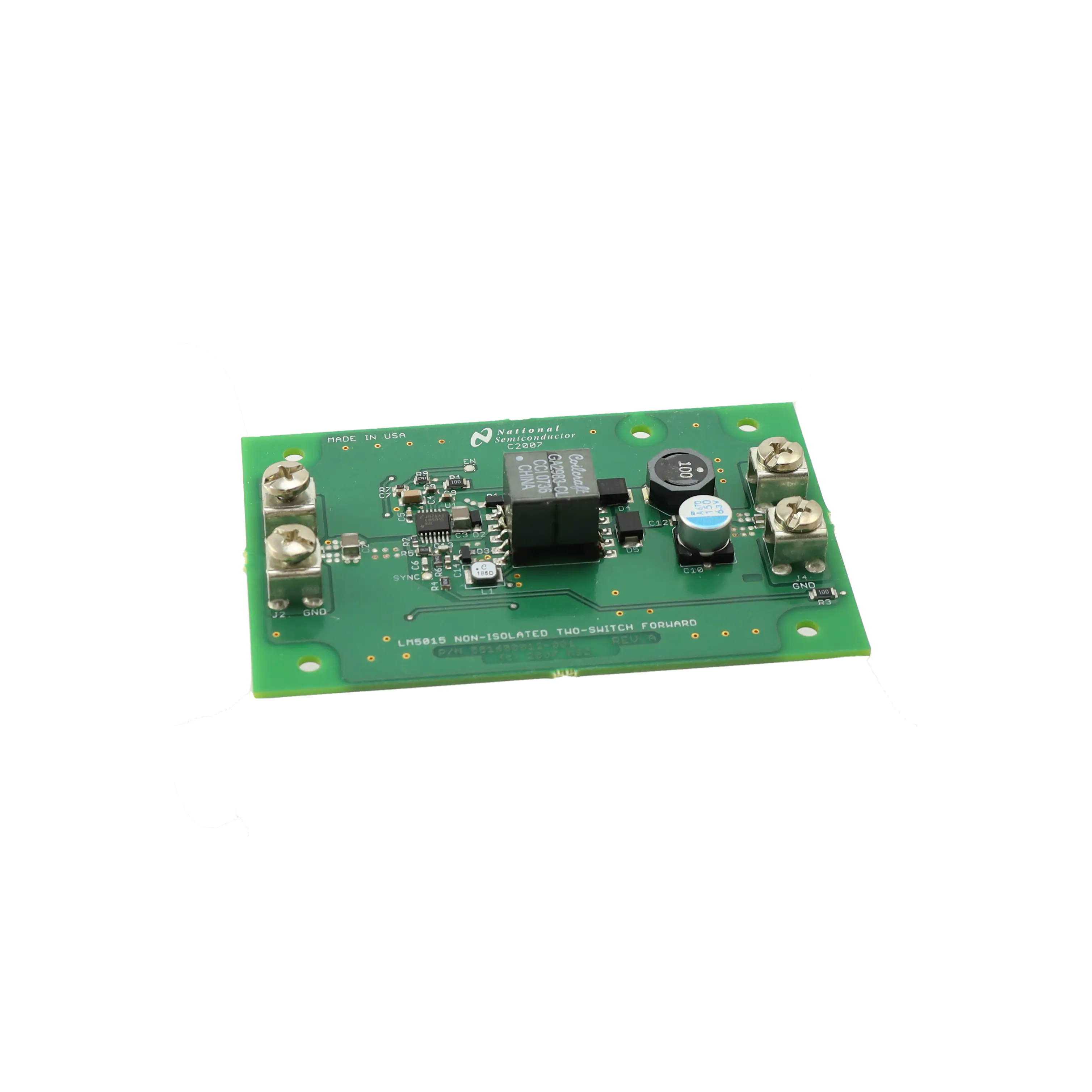
Figure 1. Evaluation Board Layout
2
Board Connections/Start-up
Figure 1 shows the PC board layout. The input connections are made to connectors J1 (high potential)
and J2 (input return). The load is connected between connectors J3 (5V) and J4 (5V return). Ensure the
wires are adequately sized for the intended load current.
A DC power supply capable of at least 75V and 0.5A is recommended as the input power source for the
evaluation board. Use the output over-voltage and over-current limit features of the DC power supply to
protect the board against damage by errant connections.
A resistive load is optimal, but an appropriate electronic load is acceptable. The maximum load current is
3A. Exceeding this current will cause the LM5015 to enter cycle-by-cycle peak current limit mode, and the
output voltage will fall below the regulated 5V. Current limit mode is triggered whenever the primary switch
current exceeds 1.2A (nominal).
During the first power up, the load should be kept reasonably low, e.g.
很抱歉,暂时无法提供与“LM5015NISOEVAL”相匹配的价格&库存,您可以联系我们找货
免费人工找货- 国内价格 香港价格
- 1+642.826791+83.09219