User's Guide
SNVA647A – May 2012 – Revised April 2013
AN-2238 LM5019 Buck Evaluation Board
1
Introduction
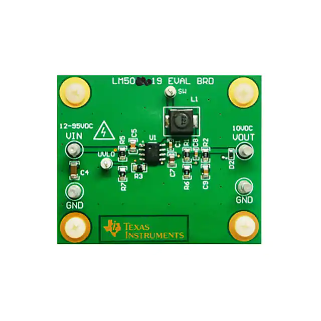
The LM5019 evaluation board provides the design engineer with a fully functional buck regulator,
employing the constant on-time (COT) operating principle. This evaluation board provides a 10V output
over an input range of 12.5V to 100V.
The board’s specifications are:
• Input Range: 12.5V to 95V, transients up to 100V (absolute maximum)
• Output Voltage: 10V
• Output Current: 100mA
• Nominal Switching Frequency ~ 440kHz
• Measured Efficiency: 85% at 100mA and VIN = 24V
• Board size: 5.5 cm x 4.5 cm
Figure 1. Evaluation Board (Top View)
All trademarks are the property of their respective owners.
SNVA647A – May 2012 – Revised April 2013
Submit Documentation Feedback
AN-2238 LM5019 Buck Evaluation Board
Copyright © 2012–2013, Texas Instruments Incorporated
1
�Theory of Operation
2
www.ti.com
Theory of Operation
Refer to the evaluation board schematic in Figure 2. When the circuit is in regulation, the buck switch is
turned on each cycle for a time determined by R3 and VIN according to the equation:
TON =
10
-10
x R3
VIN
(1)
The on-time of this evaluation board ranges from 5.56µs at VIN = 12V to 702ns at VIN = 95V. The on-time
varies inversely with input voltage. At the end of each on-time the buck switch is off for at least 144ns. In
normal operation, the off-time is much longer. During the off-time, the load current is supplied by the
output capacitor (C9). When the output voltage falls sufficiently that the voltage at FB is below 1.225V, the
regulation comparator initiates a new on-time period. For stable, fixed frequency operation, a minimum of
25mV of ripple is required at FB to switch the regulation comparator. Refer to the LM5019 100V, 100mA
Constant On-Time Synchronous Buck Regulator (SNVS788) data sheet for a more detailed block diagram,
and a complete description of the various functional blocks.
3
UVLO
The UVLO resistors (R5, R7) are selected using the following two equations:
VIN(HYS) = IHYSR5
(2)
and
VIN
(UVLO,rising)
= 1.225V x §
R5
© R7
+1·
¹
(3)
On this evaluation board R5=127kΩ and R7=14.0kΩ, resulting in UVLO rising threshold at VIN=12V and a
hysteresis of 2.5V.
SW
12V - 95V
VIN
(TP1)
LM5019
2
C4
1 F
+
R3
C5 +
R5
0.1 F 127 NŸ
237 NŸ
GND
(TP2)
UVLO/SD
4
3
BST
VIN
SW
RON
7 0.01 F
+
C1
8
L1
VOUT
220 H
UVLO
VCC
R7
14 NŸ
FB
EXP
RTN
1
R1
6.98 NŸ
6
+
U1
C8
0.1 F
+
D2
5
C7
1 F
R6
(TP3)
R2
1.5Ÿ
C9
4.7 F
1 NŸ
GND
(TP5)
Figure 2. Complete Evaluation Board Schematic for LM5019 Based Buck Converter
4
Board Connection and Start-up
The input connections are made to the TP1 (VIN) and TP2 (GND) terminals. The load is connected to the
TP3 (VOUT) AND TP5 (GND) terminals. Ensure the wires are adequately sized for the intended load
current. Before start-up a voltmeter should be connected to the input terminals, and to the output
terminals. The load current should be monitored with an ammeter or a current probe. It is recommended
that the input voltage be increased gradually to 12V, at which time the output voltage should be 10V. If the
output voltage is correct, then increase the input voltage as desired and proceed with evaluating the
circuit. DO NOT EXCEED 100V AT VIN. Caution: Do not leave EVM powered when unattended.
2
AN-2238 LM5019 Buck Evaluation Board
Copyright © 2012–2013, Texas Instruments Incorporated
SNVA647A – May 2012 – Revised April 2013
Submit Documentation Feedback
�Ripple Configuration
www.ti.com
Table 1. Bill of Materials
5
Item
Description
Mfg., Part Number
Package
Value
C5
Ceramic Capacitor
Kemet, C0805C104K1RACTU
0805
0.1uF, 100V, X7R
C7
Ceramic Capacitor
TDK, C2012X7R1C105K
0805
1uF, 16V, X7R
C8
Ceramic Capacitor
Murata, GRM188R71E104KA01D
0603
0.1uF, 25V, X7R,
0603
C9
Ceramic Capacitor
Murata, GRM21BR61E475KA12L
0805
4.7uF, 25V, X5R
D2
Diode
Diodes, Inc., SDM10U45–7–F
SOD-523
Schottky, 45V,
0.1A
Inductor
Bourns, SRR0603–221kL
6.5mm x 6.5mm
220uH, 0.310A
L1
Alternate Inductor
Wurth, 744053221
5.8mm x 5.8mm
220uH, 0.290A
Alternate Inductor
Coilcraft, LPS5030–224
5mm x 5mm
220uH, 0.245A
R1
Resistor
Vishay-Dale, CRCW08056K98FKEA
0805
220uH, 0.6A
R2
Resistor
Vishay-Dale, CRCW08051R50FKEA
0805
1.50 ohm, 1%,
0.125W
R3
Resistor
Vishay-Dale, CRCW0805237KFKEA
0805
237k ohm, 1%,
0.125W
R5
Resistor
Vishay-Dale, CRCW0805127KFKEA
0805
127k ohm, 1%,
0.125W
R6
Resistor
Vishay-Dale, CRCW08051K00FKEA
0805
1.00k ohm, 1%,
0.125W
R7
Resistor
Vishay-Dale, CRCW080514K0FKEA
0805
14.0k ohm, 1%,
0.125W
U1
Sync Switching
Regulator
Texas Instruments, LM5019
SO PowerPAD-8
100V, 100 mA
Ripple Configuration
The LM5019 is a constant-on-time (COT) buck, and requires adequate ripple at feedback (FB) node.
Three commonly used ripple generation methods are shown in Table 2.
The LM5019 evaluation board has been supplied with reduced ripple configuration (Type 2). For more
information on ripple configuration, refer to LM5019 datasheet.
Table 2. Ripple Configuration
Type 1
Lowest Cost Configuration
Type 2
Reduced Ripple Configuration
VOUT
Type 3
Minimum Ripple Configuration
VOUT
L1
VOUT
L1
L1
Cac
R FB2
R FB2
RC
To FB
R FB1
R FB1
GND
R FB2
C OUT
GND
C OUT
To FB
R FB1
GND
C8 open. Select R2:
40 mV VOUT
x
ûIL(MIN) VREF
Cr
Cac
To FB
C OUT
R2 >
Rr
RC
Select R2 and C8:
5
gSW (R1 || R6)
40 mV
R2 >
ûIL
(Not on Board)
Cr = 3300 pF
Cac = 100 nF
(VIN(MIN) ± VOUT)TON
Rr x Cr <
40 mV
C8 >
(4)
(5)
(6)
SNVA647A – May 2012 – Revised April 2013
Submit Documentation Feedback
AN-2238 LM5019 Buck Evaluation Board
Copyright © 2012–2013, Texas Instruments Incorporated
3
�Performance Curves
6
www.ti.com
Performance Curves
100
VIN=13V
VIN=24V
EFFICIENCY (%)
90
80
VIN=48V
70
60
50
40
VOUT=10V, fsw=450kHz
30
30
40
50 60 70 80 90
LOAD CURRENT (mA)
100
Figure 3. Efficiency vs Load Current
550
500
FREQUENCY (kHz)
450
400
350
300
250
200
150
100
RON=237k , VOUT=10V
50
10 20 30 40 50 60 70 80 90 100
VIN(V)
Figure 4. Frequency vs Input Voltage
Figure 5. Typical Switching Waveform (VIN=48V, Iout=100mA)
4
AN-2238 LM5019 Buck Evaluation Board
Copyright © 2012–2013, Texas Instruments Incorporated
SNVA647A – May 2012 – Revised April 2013
Submit Documentation Feedback
�PC Board Layout
www.ti.com
7
PC Board Layout
Figure 6. Board Silkscreen
Figure 7. Board Top Layer
SNVA647A – May 2012 – Revised April 2013
Submit Documentation Feedback
AN-2238 LM5019 Buck Evaluation Board
Copyright © 2012–2013, Texas Instruments Incorporated
5
�PC Board Layout
www.ti.com
Figure 8. Board Bottom Layer
6
AN-2238 LM5019 Buck Evaluation Board
Copyright © 2012–2013, Texas Instruments Incorporated
SNVA647A – May 2012 – Revised April 2013
Submit Documentation Feedback
�IMPORTANT NOTICE AND DISCLAIMER
TI PROVIDES TECHNICAL AND RELIABILITY DATA (INCLUDING DATASHEETS), DESIGN RESOURCES (INCLUDING REFERENCE
DESIGNS), APPLICATION OR OTHER DESIGN ADVICE, WEB TOOLS, SAFETY INFORMATION, AND OTHER RESOURCES “AS IS”
AND WITH ALL FAULTS, AND DISCLAIMS ALL WARRANTIES, EXPRESS AND IMPLIED, INCLUDING WITHOUT LIMITATION ANY
IMPLIED WARRANTIES OF MERCHANTABILITY, FITNESS FOR A PARTICULAR PURPOSE OR NON-INFRINGEMENT OF THIRD
PARTY INTELLECTUAL PROPERTY RIGHTS.
These resources are intended for skilled developers designing with TI products. You are solely responsible for (1) selecting the appropriate
TI products for your application, (2) designing, validating and testing your application, and (3) ensuring your application meets applicable
standards, and any other safety, security, or other requirements. These resources are subject to change without notice. TI grants you
permission to use these resources only for development of an application that uses the TI products described in the resource. Other
reproduction and display of these resources is prohibited. No license is granted to any other TI intellectual property right or to any third
party intellectual property right. TI disclaims responsibility for, and you will fully indemnify TI and its representatives against, any claims,
damages, costs, losses, and liabilities arising out of your use of these resources.
TI’s products are provided subject to TI’s Terms of Sale (www.ti.com/legal/termsofsale.html) or other applicable terms available either on
ti.com or provided in conjunction with such TI products. TI’s provision of these resources does not expand or otherwise alter TI’s applicable
warranties or warranty disclaimers for TI products.
Mailing Address: Texas Instruments, Post Office Box 655303, Dallas, Texas 75265
Copyright © 2018, Texas Instruments Incorporated
�