Product
Folder
Sample &
Buy
Support &
Community
Tools &
Software
Technical
Documents
LM5021
SNVS359E – MAY 2005 – REVISED DECEMBER 2014
LM5021 AC-DC Current-Mode PWM Controller
1 Features
3 Description
•
•
•
•
•
•
•
•
•
The LM5021 off-line pulse width modulation (PWM)
controller contains all of the features needed to
implement highly efficient off-line single-ended
flyback and forward power converters using currentmode control. The LM5021 features include an ultralow (25 µA) start-up current, which minimizes power
losses in the high voltage start-up network. A skip
cycle mode reduces power consumption with light
loads for energy conserving applications (ENERGY
STAR®, CECP, and so forth). Additional features
include under-voltage lockout, cycle-by-cycle current
limit, hiccup mode overload protection, slope
compensation,
soft-start
and
oscillator
synchronization capability. This high performance 8pin IC has total propagation delays less than 100 ns
and a 1-MHz capable oscillator that is programmed
with a single resistor.
1
•
•
•
•
•
•
Ultra-low Startup Current (25 µA Maximum)
Current Mode Control
Skip Cycle Mode for Low Standby Power
Single Resistor Programmable Oscillator
Synchronizable Oscillator
Adjustable Soft-Start
Integrated 0.7-A Peak Gate Driver
Direct Opto-Coupler Interface
Maximum Duty Cycle Limiting (80% for LM5021-1
or 50% for LM5021-2)
Slope Compensation (LM5021-1 Only)
Undervoltage Lockout (UVLO) with Hysteresis
Cycle-by-Cycle Overcurrent Protection
Hiccup Mode for Continuous Overload Protection
Leading Edge Blanking of Current Sense Signal
Packages: VSSOP-8 or PDIP-8
Device Information(1)
PART NUMBER
PACKAGE
BODY SIZE (NOM)
VSSOP (8)
3.00 mm × 3.00 mm
PDIP (8)
9.81 mm × 6.35 mm
2 Applications
LM5021
•
•
•
•
•
(1) For all available packages, see the orderable addendum at
the end of the datasheet.
DCM/CCM Flyback Converters
Industrial Power Conversion
SMPS for Smart Meters and Audio Amplifiers
Building Automation and White Goods SMPS
Isolated Telecom Power Supplies
Simplified Application Diagram
VOUT
+
AC
90 ~ 264 Vac
VCC
VIN
LM5021
RT
+
SS
COMP
OUT
CS
GND
FEEDBACK
WITH
ISOLATION
1
An IMPORTANT NOTICE at the end of this data sheet addresses availability, warranty, changes, use in safety-critical applications,
intellectual property matters and other important disclaimers. PRODUCTION DATA.
�LM5021
SNVS359E – MAY 2005 – REVISED DECEMBER 2014
www.ti.com
Table of Contents
1
2
3
4
5
6
7
Features ..................................................................
Applications ...........................................................
Description .............................................................
Revision History.....................................................
Pin Configuration and Functions .........................
Specifications.........................................................
1
1
1
2
3
4
6.1
6.2
6.3
6.4
6.5
6.6
4
4
4
4
5
7
Absolute Maximum Ratings .....................................
ESD Ratings ............................................................
Recommended Operation Conditions.......................
Thermal Information ..................................................
Electrical Characteristics...........................................
Typical Performance Characteristics ........................
7.3 Feature Description................................................. 11
7.4 Device Functional Modes........................................ 16
8
Application and Implementation ........................ 17
8.1 Application Information............................................ 17
8.2 Typical Application ................................................. 19
9 Power Supply Recommendations...................... 26
10 Layout................................................................... 26
10.1 Layout Guidelines ................................................. 26
10.2 Layout Example .................................................... 27
11 Device and Documentation Support ................. 28
Detailed Description .............................................. 9
11.1 Trademarks ........................................................... 28
11.2 Electrostatic Discharge Caution ............................ 28
11.3 Glossary ................................................................ 28
7.1 Overview ................................................................... 9
7.2 Functional Block Diagram ....................................... 10
12 Mechanical, Packaging, and Orderable
Information ........................................................... 28
4 Revision History
NOTE: Page numbers for previous revisions may differ from page numbers in the current version.
Changes from Revision D (March 2013) to Revision E
•
Added, updated, or revised the following sections: Pin Configuration and Functions; Specifications; Detailed
Description; Application and Implementation; Power Supply Recommendations; Layout; Device and Documentation
Support; and Mechanical, Packaging, and Orderable Information......................................................................................... 1
Changes from Revision C (March 2013) to Revision D
•
2
Page
Page
Changed layout of National Data Sheet to TI format ........................................................................................................... 19
Submit Documentation Feedback
Copyright © 2005–2014, Texas Instruments Incorporated
Product Folder Links: LM5021
�LM5021
www.ti.com
SNVS359E – MAY 2005 – REVISED DECEMBER 2014
5 Pin Configuration and Functions
8-Pin VSSOPand PDIP
Packages DGK and P
(Top View)
COMP
1
8
SS
VIN
2
7
RT
VCC
3
6
CS
OUT
4
5
GND
Pin Functions
PIN
I/O
DESCRIPTION
APPLICATION INFORMATION
NO.
NAME
1
COMP
I
Control input for the Pulse Width Modulator COMP pull-up is provided by an internal 5K resistor which
and Hiccup comparators.
may be used to bias an opto-coupler transistor.
2
VIN
I
Input voltage.
Input to start-up regulator. The VIN pin is clamped at 36 V
by an internal zener diode.
3
VCC
O
Output only of a linear bias supply
regulator. Nominally 8.5 V.
VCC provides bias to controller and gate drive sections of
the LM5021. An external capacitor must be connected from
this pin to ground.
4
OUT
O
MOSFET gate driver output.
High current output to the external MOSFET gate input with
source/sink current capability of 0.3 A and 0.7 A
respectively.
5
GND
—
Ground return.
6
CS
I
Current Sense input.
Current sense input for current mode control and overcurrent protection. Current limiting is accomplished using a
dedicated current sense comparator. If the CS comparator
input exceeds 0.5 V the OUT pin switches low for cycle-bycycle current limit. CS is held low for 90ns after OUT
switches high to blank the leading edge current spike.
7
RT / SYNC
O
Oscillator timing resistor pin and
synchronization input.
An external resistor connected from RT to GND sets the
oscillator frequency. This pin will also accept
synchronization pulses from an external clock.
8
SS
O
Soft-start / Hiccup time
An external capacitor and an internal 22 µA current source
set the soft-start ramp. The soft -start capacitor controls
both the soft-start rate and the hiccup mode period.
Submit Documentation Feedback
Copyright © 2005–2014, Texas Instruments Incorporated
Product Folder Links: LM5021
3
�LM5021
SNVS359E – MAY 2005 – REVISED DECEMBER 2014
www.ti.com
6 Specifications
6.1 Absolute Maximum Ratings
(1) (2)
VIN to GND
MIN
MAX
–0.3
30
V
5
mA
VIN Clamp Continuous Current
UNIT
CS to GND
–0.3
1.25
V
RT to GND
–0.3
5.5
V
All other pins to GND
–0.3
7.0
V
Operating Junction Temperature
150
Storage temperature range, Tstg
(1)
(2)
–65
150
°C
Absolute Maximum Ratings are limits beyond which damage to the device may occur. Recommended Operation Conditions are
conditions under which operation of the device is intended to be functional. For specifications and test conditions, see the Electrical
Characteristics .
If Military/Aerospace specified devices are required, please contact the Texas Instruments Sales Office/ Distributors for availability and
specifications.
6.2 ESD Ratings
V(ESD)
(1)
Human-body model (HBM), per ANSI/ESDA/JEDEC JS-001 (1)
Electrostatic discharge
VALUE
UNIT
±2000
V
JEDEC document JEP155 states that 500-V HBM allows safe manufacturing with a standard ESD control process.
6.3 Recommended Operation Conditions
over operating free-air temperature range (unless otherwise noted)
VIN Voltage
Junction Temperature
(1)
MIN
MAX
8
30
V
–40
125
°C
(1)
UNIT
After initial turn-on at VIN = 20 V.
6.4 Thermal Information
LM5021
THERMAL METRIC (1)
DGK
P
UNIT
8 PINS
RθJA
Junction-to-ambient thermal resistance
163.3
53.5
RθJC(top)
Junction-to-case (top) thermal resistance
56.7
42.9
RθJB
Junction-to-board thermal resistance
83.2
30.6
ψJT
Junction-to-top characterization parameter
5.9
20.1
ψJB
Junction-to-board characterization parameter
81.9
30.5
(1)
4
°C/W
For more information about traditional and new thermal metrics, see the IC Package Thermal Metrics application report, SPRA953.
Submit Documentation Feedback
Copyright © 2005–2014, Texas Instruments Incorporated
Product Folder Links: LM5021
�LM5021
www.ti.com
SNVS359E – MAY 2005 – REVISED DECEMBER 2014
6.5 Electrical Characteristics
MIN and MAX limits apply –40°C ≤ TJ ≤ 125°C. Unless otherwise specified: TJ= +25°C, VIN = 15 V, RT = 44.2 kΩ. (1)
PARAMETER
TEST CONDITIONS
MIN
TYP
MAX
UNIT
18
25
µA
20
23
V
STARTUP CIRCUIT
IST
Start up current
VVIN_EN
VCC Regulator enable threshold
Before VCC Enable
VVIN_DIS
VCC Regulator disable threshold
VVIN_CMP
VIN ESD clamp voltage
I = 5 mA
IVIN
Operating supply current
COMP = 0 VDC
17
7.25
30
V
36
40
2.5
3.75
mA
V
VCC SUPPLY
VVCC_EN
Controller enable threshold
6.5
7
7.5
V
VVCC_DIS
Controller disable threshold
5.3
5.8
6.3
V
VVCC
VCC regulated output
No External Load
8
8.5
9
V
VVCC_DO
VCC dropout voltage (VIN - VCC)
I = 5 mA
IVCC_LIM
VCC regulator current limit
VCC = 7.5 V
(2)
1.7
V
15
22
mA
75
125
SKIP CYCLE MODE COMPARATOR
VSKP
Skip cycle mode enable threshold
VSKP_HYS
Skip cycle mode hysteresis
⅓ [COMP - 1.25 V]
175
mV
5
mV
35
ns
CURRENT LIMIT
CS stepped from 0 to
0.6 V, time to OUT
transition low,
Cload = 0
tCS_DLY
CS limit to OUT delay
VCS_MAX
CS limit threshold
tLEB
Leading edge blanking time
90
RCS_BNK
CS blanking sinking impedance
35
55
0.45
0.5
0.55
V
ns
Ω
SOFT-START
VSS_OCV
SS pin open-circuit voltage
4.3
5.2
6.1
V
ISS
Soft-start current source
15
22
30
µA
VSS_OFF
Soft-start to COMP offset
0.35
0.55
0.75
RCOMP
COMP sinking impedance
During SS ramp
V
Ω
60
OSCILLATOR
FOSC
Frequency1 (RT = 44.2K)
135
150
165
kHz
FOSC
Frequency2 (RT = 13.3K)
440
500
560
kHz
VSYNC
Sync threshold
2.4
3.2
3.8
V
PWM COMPARATOR
tPWM_DLY
COMP to OUT delay
COMP set to 2 V
CS stepped 0 to 0.4
V, time to OUT
transition low,
Cload = 0
DMIN
Min duty cycle
COMP = 0 V
DMAX
Max duty cycle (-1 Device)
DMAX
Max duty cycle (-2 Device)
50%
KPWM
COMP to PWM comparator gain
0.33
VCOMP_OC
COMP open circuit voltage
20
0%
75%
4.2
VCOMP_MAXD COMP at max duty cycle
ICOMP
(1)
(2)
COMP short circuit current
ns
80%
5.1
85%
6
2.75
COMP = 0 V
0.6
1.1
V
V
1.5
mA
Min and Max limits are 100% production tested at 25°C. Limits over the operating temperature range are specified through correlation
using Statistical Quality Control (SQC) methods. Limits are used to calculate Average Outgoing Quality Level (AOQL).
Device thermal limitations may limit usable range.
Submit Documentation Feedback
Copyright © 2005–2014, Texas Instruments Incorporated
Product Folder Links: LM5021
5
�LM5021
SNVS359E – MAY 2005 – REVISED DECEMBER 2014
www.ti.com
Electrical Characteristics (continued)
MIN and MAX limits apply –40°C ≤ TJ ≤ 125°C. Unless otherwise specified: TJ= +25°C, VIN = 15 V, RT = 44.2 kΩ.(1)
PARAMETER
TEST CONDITIONS
MIN
TYP
MAX
UNIT
70
90
110
mV
SLOPE COMPENSATION
VSLP
Slope comp amplitude
(LM5021-1 only)
CS pin to PWM
Comparator offset at
maximum duty cycle
OUTPUT SECTION
VOUTH
OUT high saturation
IOUT = 50 mA,
VCC - OUT
0.6
1.1
V
VOUTL
OUT low saturation
IOUT = 100 mA
0.3
1
V
IO_SRC
Peak source current
OUT = VCC/2
0.3
IO_SNK
Peak sink current
OUT = VCC/2
0.7
A
tr
Rise time
Cload = 1nF
25
ns
tf
Fall time
Cload = 1nF
10
ns
A
HICCUP MODE
VOVLD
Over load detection threshold
COMP pin
VSS-OCV – 0.8
VSS-OCV – 0.6
VSS-OCV– 0.4
V
VHIC
Hiccup mode threshold
SS pin
VSS-OCV – 0.8
VSS-OCV – 0.6
VSS-OCV– 0.4
V
VRST
Hiccup mode Restart threshold
SS pin
0.1
0.3
0.5
V
IDTCS
Dead-time current source
0.1
0.25
0.4
µA
IOVCS
Overload detection timer current
source
6
10
14
µA
6
Submit Documentation Feedback
Copyright © 2005–2014, Texas Instruments Incorporated
Product Folder Links: LM5021
�LM5021
www.ti.com
SNVS359E – MAY 2005 – REVISED DECEMBER 2014
6.6 Typical Performance Characteristics
Unless otherwise specified: TJ = 25°C.
3
16
VIN Falling
12
VIN CURRENT (mA)
VIN CURRENT (PA)
14
10
8
6
4
2
1
VIN Rising
2
0
15
0
16
17
19
18
20
0
21
10
20
30
VIN (V)
VIN VOLTAGE (V)
Figure 1. VIN Start-Up Current
Figure 2. VIN UVLO
25
6
FS = 160 kHz
VCC (V)
VIN CURRENT (mA)
20
5
FS = 80 kHz
4
3
10
5
FS = 40 kHz
2
0
0
500
1000
1500
0
2000
5
10
15
20
25
OUT DRIVER LOAD (pF)
VIN (V)
Figure 3. VIN Current vs OUT Load
Figure 4. VIN Voltage Falling vs VCC Voltage
0.9
100
0.8
Sinking
10
0.7
OFF TIME (s)
OUT PEAK CURRENT (A)
15
0.6
0.5
1
0.4
0.1
Sourcing
0.3
0.2
0.01
-40
0
40
80
120
1
TEMPERATURE (oC)
10
100
1000
SOFTSTART CAPACITANCE (nF)
Figure 5. OUT Driver Current vs Temperature
Figure 6. Hiccup Mode Deadtime vs Softstart Capacitance
Submit Documentation Feedback
Copyright © 2005–2014, Texas Instruments Incorporated
Product Folder Links: LM5021
7
�LM5021
SNVS359E – MAY 2005 – REVISED DECEMBER 2014
www.ti.com
Typical Performance Characteristics (continued)
Unless otherwise specified: TJ = 25°C.
OUT SWITCHING FREQUENCY (kHz)
1000
LM5021-1
LM5021-2
100
10
1
10
100
1000
RT (kQ)
Figure 7. Output Switching Frequency vs RT
8
Submit Documentation Feedback
Copyright © 2005–2014, Texas Instruments Incorporated
Product Folder Links: LM5021
�LM5021
www.ti.com
SNVS359E – MAY 2005 – REVISED DECEMBER 2014
7 Detailed Description
7.1 Overview
The LM5021 is a single ended current mode controller primarily intended for use in offline forward or flyback
converters. It is also useful for boost converters. Low startup current and a wide UVLO hysteresis make low
dissipation startup circuits simple to implement. An on board 7-V regulator supplies stable power for device
operation and can supply external circuitry. A soft start function minimizes stresses during startup and allows the
converter to come to steady state operating conditions gradually.
The device comes in two versions with different maximum duty cycles. The LM5021-1 has a maximum duty cycle
of 80% while the LM5021-2 has a maximum duty cycle of 50%. For current mode control applications where the
duty cycle can exceed 50%, slope compensation is implemented by simply adding a resistor between the
LM5021-1 CS pin and the current sense filter capacitor.
Cycle-by-cycle overcurrent sensing provides robust protection. A 500-mV maximum current sense threshold
minimizes power dissipation in supplies that sense the main switch current directly with a resistor. For a
sustained overcurrent condition, the controller will enter a hiccup mode to reduce component stresses. The
controller automatically restarts when the overload condition is removed.
The switching frequency is programmable using a single resistor connected from the RT pin to GND. For
applications that require it, the switching frequency can be synchronized to an external clock source by
capacitively coupling a pulse train into the RT pin.
Skip cycle operation is implemented to reduce input power and increase efficiency at light load conditions. For
applications where this is not desirable, skip cycle operation may be disabled by adding an offset voltage to the
CS pin.
Submit Documentation Feedback
Copyright © 2005–2014, Texas Instruments Incorporated
Product Folder Links: LM5021
9
�LM5021
SNVS359E – MAY 2005 – REVISED DECEMBER 2014
www.ti.com
7.2 Functional Block Diagram
8.5V LINEAR
REGULATOR
VIN
2
VIN UVLO
20V RISING
7.25V FALLING
36V
CLAMP
VCC
3
VCC UVLO
7V RISING
5.8V FALLING
EN
VCC_UVLO
DIS
CLK
VCC_UVLO
RT/ SYNC
7
OSC
VCC_UVLO
SLOPE COMPENSATION RAMP GENERATOR
(LM5021 - 1 ONLY)
MAX DUTY LIMIT
LM5021 - 1 (80%)
LM5021 - 2 (50%)
50 PA
0 PA
PWM
COMPARATOR
5.2V
5k
COMP
1
S
DRIVER
Q
OUT
4
R
+
1.25V
2R
PWM
LOGIC
-
R
SKIP CYCLE
COMPARATOR
550 mV
5.2V
+
-
22 PA
+
SS
125 mV
CS
6
1.8k
COMP
CURRENT LIMIT
COMPARATOR
SOFTSTART
AND
HICCUP
MODE
LOGIC
+
SS
8
0.25 PA
10 PA
500 mV
CLK
Leading Edge Blanking
VCC_UVLO
GND
5
10
Submit Documentation Feedback
Copyright © 2005–2014, Texas Instruments Incorporated
Product Folder Links: LM5021
�LM5021
www.ti.com
SNVS359E – MAY 2005 – REVISED DECEMBER 2014
7.3 Feature Description
7.3.1 PWM Comparator and Slope Compensation
The PWM comparator compares the current sense signal with the loop error voltage from the COMP pin. The
COMP pin voltage is reduced by 1.25 V then attenuated by a 3:1 resistor divider. The PWM comparator input
offset voltage is designed such that less than 1.25 V at the COMP pin will result in a zero duty cycle at the
controller output.
For duty cycles greater than 50 percent, current mode control circuits are subject to sub-harmonic oscillation. By
adding an additional fixed slope voltage ramp signal (slope compensation) to the current sense signal, this
oscillation can be avoided. The LM5021-1 integrates this slope compensation by summing a ramp signal
generated by the oscillator with the current sense signal. The slope compensation is generated by a current ramp
driven through an internal 1.8 kΩ resistor connected to the CS pin. Additional slope compensation may be added
by increasing the resistance between the current sense filter capacitor and the CS pin, thereby increasing the
voltage ramp created by the oscillator current ramp. Since the LM5021-2 is not capable of duty cycles greater
than 50%, there is no slope compensation feature in this device.
7.3.2 Current Limit and Current Sense
The LM5021 provides a cycle-by-cycle over current protection feature. Current limit is triggered by an internal
current sense comparator threshold which is set at 500 mV. If the CS pin voltage plus the slope compensation
voltage exceeds 500 mV, the OUT pin output pulse will be immediately terminated.
An RC filter, located near the LM5021, is recommended for the CS pin to attenuate the noise coupled from the
power FET's gate to source. The CS pin capacitance is discharged at the end of each PWM clock cycle by an
internal switch. The discharge switch remains on for an additional 90ns leading edge blanking interval to
attenuate the current sense transient that occurs when the external power FET is turned on. In addition to
providing leading edge blanking, this circuit also improves dynamic performance by discharging the current
sense filter capacitor at the conclusion of every cycle.
The LM5021 CS comparator is very fast, and may respond to short duration noise pulses. Layout considerations
are critical for the current sense filter and sense resistor. The capacitor associated with the CS filter must be
placed very close to the device and connected directly to the pins of the IC (CS and GND). If a current sense
transformer is used, both leads of the transformer secondary should be routed to the sense resistor, which
should also be located close to the IC. If a current sense resistor located in the power FET's source is used for
current sense, a low inductance resistor is required. In this case, all of the noise sensitive low current grounds
should be connected in common near the IC and then a single connection should be made to the power ground
(sense resistor ground point).
7.3.3 Oscillator, Shutdown and Sync Capability
A single external resistor connected between RT and GND pins sets the LM5021 oscillator frequency. The
LM5021-2 device, with 50% maximum duty cycle, includes an internal flip-flop that divides the oscillator
frequency by two. This method produces a precise 50% maximum duty cycle limit. Because of this frequency
divider, the oscillator frequency of the LM5021-2 is actually twice the frequency of the gate drive output (OUT).
For the LM5021-1 device, the oscillator frequency and the operational output frequency are the same. To set a
desired output switching frequency (Fsw), the RT resistor can be calculated from:
LM5021-1:
RT =
6.63 x 10⁹
FSW
(1)
LM5021-2:
RT =
6.63 x 10⁹
2 x FSW
(2)
Submit Documentation Feedback
Copyright © 2005–2014, Texas Instruments Incorporated
Product Folder Links: LM5021
11
�LM5021
SNVS359E – MAY 2005 – REVISED DECEMBER 2014
www.ti.com
Feature Description (continued)
The LM5021 can also be synchronized to an external clock. The external clock must have a higher frequency
than the free running oscillator frequency set by the RT resistor. The clock signal should be capacitively coupled
into the RT pin with a 100pF capacitor. A peak voltage level greater than 3.8 V at the RT pin is required for
detection of the sync pulse. The dc voltage across the RT resistor is internally regulated at 2 V. Therefore, the ac
pulse superimposed on the RT resistor must have 1.8-V or greater amplitude to successfully synchronize the
oscillator. The sync pulse width should be set between 15 ns to 150 ns by the external components. The RT
resistor is always required, whether the oscillator is free-running or externally synchronized. The RT resistor
should be located very close to the device and connected directly to the pins of the LM5021 (RT and GND).
7.3.4 Gate Driver and Max Duty Cycle Limit
The LM5021 provides a gate driver (OUT), which can source peak current of 0.3A and sink 0.7A. The LM5021 is
available in two duty-cycle limit options. The maximum output duty-cycle is typically 80% for the LM5021-1
option, and precisely equal to 50% for the LM5021-2 option. The maximum duty cycle function for the LM5021-2
is accomplished with an internal toggle flip-flop to ensure an accurate duty cycle limit. The internal oscillator
frequency of the LM5021-2 is therefore twice the switching frequency of the PWM controller (OUT pin).
The 80% maximum duty-cycle function for the LM5021-1 is determined by the internal oscillator. For the
LM5021-1 the internal oscillator frequency and the switching frequency of the PWM controller are the same.
7.3.5 Soft-Start
The soft-start feature allows the power converter to gradually reach the initial steady state operating point, thus
reducing start-up stresses and current surges. An internal 22 µA current source charges an external capacitor
connected to the SS pin. The capacitor voltage will ramp up slowly, limiting the COMP pin voltage and the duty
cycle of the output pulses. The soft-start capacitor is also used to generate the hiccup mode delay time when the
output of the switching power supply is continuously overloaded.
7.3.6 Hiccup Mode Overload Current Limiting
Hiccup mode is a method of protecting the power supply from over-heating and damage during an extended
overload condition. When the output fault is removed the power supply will automatically restart.
Figure 8, Figure 9, and Figure 10 illustrate the equivalent circuit of the hiccup mode for LM5021 and the relevant
waveforms. During start-up and in normal operation, the external soft-start capacitor Css is pulled up by a current
source that delivers 22 µA to the SS pin capacitor. In normal operation, the soft-start capacitor continues to
charge and eventually reaches the saturation voltage of the current source (VSS_OCV, nominally 5.2 V). During
start-up the COMP pin voltage follows the SS capacitor voltage and gradually increases the peak current
delivered by the power supply. When the output of the switching power supply reaches the desired voltage, the
voltage feedback amplifier takes control of the COMP signal (via the opto-coupler). In normal operation the
COMP level is held at an intermediate voltage between 1.25 V and 2.75 V controlled by the voltage regulation
loop. When the COMP pin voltage is below 1.25 V, the duty-cycle is zero. When the COMP level is above 2.75
V, the duty cycle will be limited by the 0.5-V threshold of cycle-by-cycle current limit comparator.
If the output of the power supply is overloaded, the voltage regulation loop demands more current by increasing
the COMP pin control voltage. When the COMP pin exceeds the over voltage detection threshold (VOVLD,
nominally 4.6 V), the SS capacitor Css will be discharged by a 10 µA overload detection timer current source,
IOVCS. If COMP remains above VOVLD long enough for the SS capacitor to discharge to the Hiccup mode
threshold (VHIC, nominally 4.6 V), the controller enters the hiccup mode. The OUT pin is then latched low and the
SS capacitor discharge current source is reduced from 10 µA to 0.25 µA, the dead-time current source, IDTCS.
The SS pin voltage is slowly reduced until it reaches the Restart threshold (VRST, nominally 0.3 V). Then a new
start-up sequence commences with 22 µA current source charging the capacitor CSS. The slow discharge of the
SS capacitor from the Hiccup threshold to the Restart threshold provides an extended off time that reduces the
overheating of components including diodes and MOSFETs due to the continuous overload. The off time during
the hiccup mode can be calculated from the following equation:
CSS x (VHC - VRST)
Toff =
12
IDTCS
CSS x (4.6V - 0.3V)
=
0.25 PA
Submit Documentation Feedback
(3)
Copyright © 2005–2014, Texas Instruments Incorporated
Product Folder Links: LM5021
�LM5021
www.ti.com
SNVS359E – MAY 2005 – REVISED DECEMBER 2014
Feature Description (continued)
Example:
Toff = 808 ms, assuming the CSS capacitor value is 0.047 µF
Short duration intermittent overloads will not trigger the hiccup mode. The overload duration required to trigger
the hiccup response is set by the capacitor CSS, the 10 µA discharge current source and voltage difference
between the saturation level of the SS pin and the Hiccup mode threshold. Figure 10 shows the waveform of SS
pin with a short duration overload condition. The overload time required to enter the hiccup mode can be
calculated from the following equation:
CSS x (VSS_OCV - VHC)
=
Toverload =
CSS x 0.6V
10 PA
IOVCS
(4)
Example:
Toverload = 2.82 ms, assuming the CSS capacitor value is 0.047 µF
5.2V
COMP
OVERLOAD
DETECTION
550 mV
5.2V
+
4.6V
-
EN
22 PA
+
SS
EN
S
+
4.6V
10 PA
EN
Q
0.25 PA
R
HICCUP MODE
COMPARATOR
0.3V
OUT
PWM
DRIVER
+
-
RESTART
COMPARATOR
Figure 8. Hiccup Mode Control
Submit Documentation Feedback
Copyright © 2005–2014, Texas Instruments Incorporated
Product Folder Links: LM5021
13
�LM5021
SNVS359E – MAY 2005 – REVISED DECEMBER 2014
www.ti.com
Feature Description (continued)
Normal
operation
Soft-Start
Overload
Detection
SMPS latched
OFF
Soft-Start
COMP
-10 PA
5.2V
4.6V
SS
+22 PA
-0.25 PA
+22 PA
0.3V
Figure 9. Waveform at SS and COMP Pin due to Continuous Overload
COMP
5.2V
4.6V
SS
-10 PA
+22 PA
during over
+22 PA
after releasing the over load
load
Figure 10. Waveform at SS and COMP Pin due to Brief Overload
7.3.7 Skip Cycle Operation
During light load conditions, the efficiency of the switching power supply typically drops as the losses associated
with switching and operating bias currents of the converter become a significant percentage of the power
delivered to the load. The largest component of the power loss is the switching loss associated with the gate
driver and external MOSFET gate charge. Each PWM cycle consumes a finite amout of energy as the MOSFET
is turned on and then turned off. These switching losses are proportional to the frequency of operation. The Skip
Cycle function integrated within the LM5021 controller reduces the average switching frequency to reduce
switching losses and improve efficiency during light load conditions.
When a light load condition occurs, the COMP pin voltage is reduced by the voltage feedback loop to reduce the
peak current delivered by the controller. Referring to Figure 11, the PWM comparator input tracks the COMP pin
voltage through a 1.25 V level shift circuit and a 3:1 resistor divider. As the COMP pin voltage falls, the input to
the PWM comparator falls proportionately. When the PWM comparator input falls to 125 mV, the Skip Cycle
comparator detects the light load condition and disables output pulses from the controller. The controller
continues to skip switching cycles until the power supply output falls and the COMP pin voltage increases to
demand more output current. The number of cycles skipped will depend on the load and the response time of the
14
Submit Documentation Feedback
Copyright © 2005–2014, Texas Instruments Incorporated
Product Folder Links: LM5021
�LM5021
www.ti.com
SNVS359E – MAY 2005 – REVISED DECEMBER 2014
Feature Description (continued)
frequency compensation network. Eventually the COMP voltage will increase when the voltage loop requires
more current to sustain the regulated output voltage. When the PWM comparator input exceeds 130 mV (5 mV
hysteresis), normal fixed frequency switching resumes. Typical power supply designs will produce a short burst
of output pulses followed by a long skip cycle interval. The average switching frequency in the Skip Cycle mode
can be a small fraction of the normal operating frequency of the power supply.
The skip cycle mode of operation can be disabled by adding an offset voltage to the CS pin (refer to Figure 12).
A resistive divider connected to a regulated source, injecting a 125 mV offset (minimum) on the CS pin, will force
the voltage at the PWM Comparator to be greater than 125 mV, disabling the Skip Cycle Comparator.
5.2V
5k
COMP
1.25V
+
PWM
COMPARATOR
2R
PWM
LOGIC
-
R
+
SKIP CYCLE
COMPARATOR
125 mV
CS
1.8k
+
CLK LEADING EDGE
BLANKING
-
CURRENT LIMIT
COMPARATOR
500 mV
Figure 11. Skip Cycle Control
VIN
OUT
LM5021
Voffset > 125 mV
CS
VCC
RSense
Figure 12. Disabling the Skip Cycle Mode
Submit Documentation Feedback
Copyright © 2005–2014, Texas Instruments Incorporated
Product Folder Links: LM5021
15
�LM5021
SNVS359E – MAY 2005 – REVISED DECEMBER 2014
www.ti.com
7.4 Device Functional Modes
7.4.1 Operation With VIN Below 20 V
When a converter is first powered up, there is typically no voltage present on the VIN pin of the controller and the
controller is in a low current startup mode. In this mode, there is no activity at the OUT pin and the device is
internally in a shutdown mode that consumes minimal current, typically 18 µA. The startup circuit must be
capable of supplying the maximum startup current of 25 µA, plus additional current to charge the VIN capacitor to
20 V in any required startup time, at the minimum desired startup voltage for the converter. Once the VIN voltage
reaches the startup voltage of 20 V, normal operation in soft start commences. The converter will continue to
operate until the VIN voltage falls below the turn off threshold of 7.25 V
7.4.2 Operation in Soft Start
Soft-start mode occurs after the VIN pin reaches the startup voltage after being below 7.25 V or after a hiccup
overcurrent cycle. In this mode the reference voltage applied to the PWM comparator from the COMP pin is
clamped and allowed to rise at a rate determined by the charging of a capacitor connected to the SS pin. This
ramped voltage controls the amount of peak current in the power stage and allows it to increase slowly to reduce
stresses on system components. When the clamp level exceeds the level required by the voltage applied to the
COMP pin externally, the external feedback circuitry supplying the voltage on COMP assumes control pf the
power stage peak current.
7.4.3 Operation Under Normal Conditions
Once the converter has completed soft start, it operates at either a fixed switching frequency with the output
pulse width determined by the voltage applied to the COMP pin and the ramp applied to the CS pin, or in a skip
cycle mode when the converter load is light. For the normal fixed frequency mode of operation the output is set
high when the oscillator starts a new clock cycle (or every other clock cycle in the LM5021-2). The CS pin is
connected to the current sensing network for the converter and the voltage on that pin is compared to one-third
of the voltage applied to the COMP pin less 1.25 V (see the Functional Block Diagram section) from the external
error amplifier and compensation circuit. The CS pin signal should be a linearly increasing ramp proportional to
the current in the power stage of the converter. The output pulse terminates when the voltage at the CS pin
exceeds one-third of the voltage on COMP less 1.25 V.
7.4.4 Operation in Skip Cycle
During periods of minimal output power demand, the controller will operate in a skip cycle mode to reduce power
consumption and increase efficiency at lighter loads. Skip cycle mode is entered when in normal operation the
voltage on COMP is reduced by the external error amplifier to the point that the voltage on the PWM comparator
falls below 125 mV. This will typically be about 1.625 V or lower at the COMP pin. When this mode is entered,
the controller inhibits pulses on the output until the error amplifier and compensation circuit requires
approximately 130 mV at the input of the PWM comparator. This is approximately 1.64 V at the COMP pin. The
number and frequency of pulses in the skip cycle mode is dependent on the load and response time of the
external error amplifier and compensation circuit. Skip cycle operation may be disabled by adding a 125-mV DC
offset to the CS pin.
7.4.5 Operation at Overload
If the load on the converter increases beyond design limitations, the converter can fail due to component over
stress. The LM5021 uses a fixed maximum CS pin voltage of 500 mV to limit the amount of current in the
converter power stage. The output pulse will terminate when the CS pin voltage exceeds this threshold
regardless of the current command voltage applied to the COMP pin. For short time duration overload events,
the converter will operate normally with typically a small transient drop in output voltage that is corrected by the
error amplifier when the overload is removed. If the overload is longer in duration, the error amplifier will apply
higher and higher voltage to the COMP pin as the output voltage sags. If the COMP pin voltage exceeds the
overload threshold of 4.6 V, the converter will enter hiccup mode.
7.4.6 Operation in Hiccup Mode
If during an overload, the COMP pin voltage rises above 4.6 V, hiccup mode operation is started. In this mode,
the OUT pin is held low and the soft start capacitor is discharged using a 10-µA current source. When the soft
start capacitor discharges to 0.3 V, a new startup sequence begins with the controller in the soft start mode.
16
Submit Documentation Feedback
Copyright © 2005–2014, Texas Instruments Incorporated
Product Folder Links: LM5021
�LM5021
www.ti.com
SNVS359E – MAY 2005 – REVISED DECEMBER 2014
8 Application and Implementation
NOTE
Information in the following applications sections is not part of the TI component
specification, and TI does not warrant its accuracy or completeness. TI’s customers are
responsible for determining suitability of components for their purposes. Customers should
validate and test their design implementation to confirm system functionality.
8.1 Application Information
8.1.1 Startup Circuit
Referring to Figure 13, the input capacitor CVIN is trickle charged through the start-up resistor Rstart, when the
rectified ac input voltage HV is applied. The VIN current consumed by the LM5021 is only 18 µA (nominal) while
the capacitor CVIN is initially charged to the start-up threshold. When the input voltage, VIN reaches the upper
VIN UVLO threshold of 20 V, the internal VCC linear regulator is enabled. The VCC regulator will remain on until
VIN falls to the lower UVLO threshold of 7.25 V (12.5 V hysteresis). When the VCC regulator is turned on, the
external capacitor at the VCC pin begins to charge. The PWM controller, soft-start circuit and gate driver are
enabled when the VCC voltage reaches the VCC UVLO upper threshold of 7 V. The VCC UVLO has 1.2 V
hysteresis between the upper and lower thresholds to avoid chattering during transients on the VCC pin. When
the VCC UVLO enables the switching power supply, energy is transferred from the primary to the secondary
transformer winding(s). A bias winding, shown in Figure 13, delivers power to the VIN pin to sustain the VCC
regulator. The voltage supplied should be from 11 V (VCC regulated voltage maximum plus VCC regulator
dropout voltage) to 30 V (maximum operating VIN voltage). The bias winding should always be connected to the
VIN pin as shown in Figure 13. Do not connect the bias winding to the VCC pin. The start-up sequence is
completed and normal operation begins when the voltage from the bias winding is sufficient to maintain VCC
level greater than the VCC UVLO threshold (5.8 V typical).
The LM5021 is designed for ultra-low start-up current into the VIN pin. To achieve this very low start-up current,
the VCC regulator of the LM5021 is unique as compared to the VCC regulator used in other controllers of the
LM5xxx family. The LM5021 is designed specifically for applications with the bias winding connected to the VIN
pin as shown in Figure 13.
NOTE
It is not recommended that the bias winding be connected to the VCC pin of the LM5021.
Doing so can cause the device to operate incorrectly or not at all.
The size of the start-up resistor Rstart not only affects power supply start-up time, but also power supply
efficiency since the resistor dissipates power in normal operation. The ultra low start-up current of the LM5021
allows a large value Rstart resistor (up to 3 MΩ) for improved efficiency with reasonable start-up time.
HV
Rstart
TRANSFORMER
BIAS
WINDING
VCC
REGULATOR
VIN
VCC
+
CVIN
VIN
UVLO
UPPER
S
LOWER
R
Q
VCC
UVLO
CVCC
INTERNAL
BIAS
GENERATOR
Enable Driver
Figure 13. Start-Up Circuit Block Diagram
Submit Documentation Feedback
Copyright © 2005–2014, Texas Instruments Incorporated
Product Folder Links: LM5021
17
�LM5021
SNVS359E – MAY 2005 – REVISED DECEMBER 2014
www.ti.com
Application Information (continued)
8.1.2 Relationship Between Input Capacitor CIN and VCC Capacitor CVCC
The internal VCC linear regulator is enabled when VIN reaches 20 V. The drop in VIN due to charge transfer
from CVIN to CVCC after the regulator is enabled can be calculated from the following equations where VIN' is the
voltage on CVIN immediately after the VCC regulator charges CVCC.
ΔVIN x CVIN = ΔVCC x CVCC
(20 V – VIN') CVIN = 8.5V CVCC
VIN = 20V - 8.5V x
(5)
(6)
CVCC
CVIN
(7)
Assuming CVIN value as 10 µF, and CVCC of 1µF, then the drop in VIN will be 0.85 V, or the VIN value drops to
19.15 V. The value of the VCC capacitor can be small (less than 1 uF) as it supplies only transient gate drive
current of a short duration. The CVIN capacitor must be sized to supply the gate drive current and the quiescent
current of LM5021, until the transformer bias winding delivers sufficient voltage to VIN to sustain the VCC
voltage.
The CVIN capacitor value can be calculated from the operating VCC load current after its output voltage reaches
the VCC UVLO threshold. For example, if the LM5021 is driving an external MOSFET with total gate charge (Qg)
of 25nC, the average gate drive current is Qg x Fsw, where Fsw is the switching frequency. Assuming a
switching frequency of 150KHz, the average gate drive current is 3.75 mA. Since the IC consumes approximately
2.5 mA operating current in addition to the gate current, the total current drawn from CVIN capacitor is the
operating current plus the gate charge current, or 6.25 mA. The CVIN capacitor must supply this current for a brief
time until the transformer bias winding takes over. The CVIN voltage must not fall below 8.5 V during the start-up
sequence or the cycle will be restarted. The maximum allowable start-up time can be calculated using the value
of CVIN, the change in voltage allow at VIN (19.15 V – 8.5 V) and the VCC regulator current (6.25 mA). Tmax, the
maximum time allowed to energize the bias winding is:
CVIN x (19.15V - 8.5V)
= 17 ms
Tmax =
6.25 mA
(8)
If the calculated value of Tmax is too small, the value of Cin should be increased further to allow more time
before the transformer bias winding takes over and delivers the operating current to the VCC regulator.
Increasing CVIN will increase the time from the application of the rectified ac (HV in Figure 13) to the time when
VIN reaches the 20 V start threshold. The initial charging time of CVIN is:
TVIN_THRESHOLD = RSTART x CVIN x ln
18
1-
20V
HV
-1
Submit Documentation Feedback
(9)
Copyright © 2005–2014, Texas Instruments Incorporated
Product Folder Links: LM5021
�LM5021
www.ti.com
SNVS359E – MAY 2005 – REVISED DECEMBER 2014
8.2 Typical Application
C1
2200p
NOTES:
1)
Do not populate
1
TP1
U_BULK
R3
S10K175E2K1
85Vac-130Vac Input
1
3
J1
1
C2
2200p
10mH
C3
1
470n
2
D3
DF06S
R4
2.5
L1
D1
US1G
C4
+
82u
350V
R1
1.5M
4
180Vac for 35ms
R2
10k
R5
1.5M
1
C11
R9
100k
1
220p
4kV Isolation barier
C5
Q1
BSS127
100p
R6
R8
2
100
R7
10
TP2
T1
85 uH
TP4
24V
TP5
TP3
L2
4
14
C6
D5
10n
Isat > 2.4A
1
Q2
MMBT2222A
15
1
D7
BZX585-C10
R10
47k
6
D8
12
C10
+
Program
100n
6.8u
GND
220u
Program pin 0V -> Vout=24V
1
Q3
MMBT2222A
TP6
C12 TS4148 RZ
C13
R12
22k
1u
24V/1.45A 2%
C9
C8
Program pin open -> Vout=8V
ES1D
D6
TP7
1
C7
220u
D4
20CTQ150
7
VIN
1
+
11
2
1
J2
1uH
3
BZX585-C27
+
22u
PROGRAM
50V
1
D9
BZX585-C15
U1
LM5021-2
8 SS
Fsw = 145kHz
7
6
C14
R17
5
C15
220n
22.1k
RT
VIN
CS
VCC
GND
OUT
1
1
2
TP8 +8V
TP8 -> 8V
TP9
1
Q4
STP11NK40ZFP
3
R16
4
5.1V
4.7
+8V
C17
150pF
1
1
COMP
HS1
1uF
1
1
C18
R22
1
R15
13k
100k
D10
R21
tbd
1
R14
1n
500V
100
R19 for development purpose only
R20
100
TP11
R33
76.8k
C16
TLV431BDBZ
TP10
U_BULK
100n
R19
49.9
R34
24.3k
R23
0.2
5.1V
C19
1
5
4
43.2k
1
R26
4.7k
C21
R24
100n
U4
CNY17F-3M
2
TP12
5
U3
OPA170AIDBV
R25
69.8k
TP13
3
1
4
1
R27
2
R28
1
1
R30
21k
6.34k
C23
100p
C24
1n
100k
Q5
BSS138
C20
1u
R31
100
R32
221k
C25
1n
Figure 14. Typical Application Circuit
Submit Documentation Feedback
Copyright © 2005–2014, Texas Instruments Incorporated
Product Folder Links: LM5021
19
�LM5021
SNVS359E – MAY 2005 – REVISED DECEMBER 2014
www.ti.com
8.2.1 Design Requirements
DESIGN PARAMETER
VALUE
Input voltage range
85 Vac - 130 Vac
Output voltage
24 Vdc or 8 Vdc (programmable)
Output current
1.45 Adc at 24 Vdc
Switching frequency
145 kHz
Maximum duty cycle
50%
Isolation level
4 kV
Footprint
68 mm × 34 mm
8.2.2 Detailed Design Procedure
8.2.2.1 Primary Bulk Capacitance
The primary side bulk cap, C4, is selected based on the power level and the desired minimum bulk voltage level.
The bulk capacitor value can be calculated as:
é
1
VBULK(min) ù
2PIN ´ ê0.25 + ´ arcsin(
)ú
p
2 ´ VIN(min) û
ë
C4 =
2
2
- VBULK(min)
(2VIN(min)
) ´ fLINE
where
•
•
•
•
PIN is the maximum input power. Input power is the maximum output power divided target efficiency.
VIN(min) is the minimum AC input voltage RMS value.
VBULK(min) is the target minimum bulk voltage.
fLINE is the line frequency.
(10)
Based on the equation, to achieve 70-V minimum bulk voltage, the bulk capacitor should be larger than 72 µF
and 82 µF was chosen in the design.
8.2.2.2 Transformer
The transformer design starts with selecting a suitable switching frequency. Generally, the switching frequency
selection is based on the tradeoff between the converter size and efficiency. Higher switching frequency results
in smaller transformer size, but the switching losses will increase, potentially impacting efficiency. Sometimes,
the switching frequency is selected to avoid certain frequencies or harmonics that could interfere with those used
for communication. The frequency selection is beyond the scope of this datasheet.
EMI regulations place limits on EMI noise at 150 kHz and higher. For this design, 145 kHz is selected for the
switching frequency to minimize transformer size while keeping the switching frequency below the EMI regulation
band.
The transformer turns ratio can be selected based on the desired MOSFET voltage rating and diode voltage
rating. Since the maximum input voltage is 130 V AC, the peak bulk voltage can be calculated as:
VBULK(max) = √ 2 × VIN(max) = 184 V
(11)
To take advantage of the low Rdson of lower voltage MOSFETs, a target device rating of 400 V is selected.
Considering the design margin and extra voltage ringing on the MOSFET drain, the reflected output voltage
should be less than 50 V. The transformer primary to secondary (nPS) turns ratio can be selected as:
50
nPS =
= 2.083
(12)
24
The output rectifier diode (D4) voltage stress is also affected by the turns ratio. The stress applied to the diode is
the output voltage plus the reflected input voltage. The voltage stress on the diode can be calculated as:
VBULK(max)
184 V
VD4 =
+ VOUT =
+ 24 V = 112 V
nps
2.083
(13)
20
Submit Documentation Feedback
Copyright © 2005–2014, Texas Instruments Incorporated
Product Folder Links: LM5021
�LM5021
www.ti.com
SNVS359E – MAY 2005 – REVISED DECEMBER 2014
Considering the ringing voltage spikes always present in a switching power supply and allowing for voltage
derating (normally 80% derating is used), the diode voltage rating should be higher than 150 V.
The transformer inductance selection is based on the requirement for this converter to remain in discontinuous
conduction (DCM). Selecting a larger inductance would allow the converter operate in continuous conduction
(CCM). CCM operation tends to increase the transformer size. The primary inductance (Lm) can be calculated as:
2
nPSVOUT
æ
ö
2
VBULK(min)
´ç
1
VBULK(min) + nPSVOUT ÷ø
è
Lm =
2
50% ´ PIN ´ fSW
(14)
In this equation, fsw is the 145-kHz switching frequency. Therefore, the transformer inductance should be
selected as 85 µH.
The auxiliary winding provides the power for LM5021 during normal operation. The auxiliary winding voltage is
the output voltage reflected to the primary side. A higher reflected voltage allows the IC to quickly get energy
from the transformer during startup and makes starting a heavy or highly capacitive load easier. However, a high
auxiliary reflected voltage makes the IC consume more power, reducing efficiency and increasing standby power
consumption. Therefore, a tradeoff is required. In this design, the auxiliary winding voltage is selected to ensure
that there is enough voltage available to ensure the controller will operate when the output voltage is
programmed to the lower 8-V setting. Therefore, the auxiliary winding to the output winding turns ratio is selected
as:
12V
nAS =
= 1.5
8V
(15)
8.2.2.3 Main Switch FET and Output Rectifier
Based on calculated inductor value and the switching frequency, the current stress of the MOSFET (Q4) and
diode (D4) can be calculated.
The peak current of Q4 can be calculated as:
IPK _ Q4 =
PIN
VBULK(min) ´
nPS VOUT
VBULK(min) + nPS VOUT
nPSVOUT
1 VBULK(min) VBULK(min) + nPSVOUT
+
´
2 Lm
fSW
(16)
The peak current is 2.55 A.
The peak current in D4 is the peak current in Q4 reflected to the secondary side:
ID4 = NPS × IQ4 = 5.3 A
(17)
The RMS current in Q4 can be calculated as:
2
IQ4 _ RMS =
1 3 æ VBULK(min) ö
D2IPK _ Q4 VBULK(min)
2
D ´ç
+ D ´ IPK
_ Q4
÷
3
Lm ´ fSW
è Lm ´ fSW ø
(18)
Here D is the Q4 on time duty cycle at minimum bulk voltage and it can be calculated as:
nPSVOUT
D=
VBULK(min) + nPSVOUT
(19)
The RMS current in Q4 is 0.97 A. Therefore, STP11NK40ZFP is selected.
The average current in D4 is the output current 1.45 A. With a 150-V reverse voltage rating and a 20-A average
current rating, 20CTQ150 is selected.
The output capacitor is selected based on the output voltage ripple requirement. In this design, 0.1% voltage
ripple is assumed. Based on the 0.1% ripple requirement, the capacitor value can be selected based on:
nPSVOUT
IOUT ´
VBULK(min) + nPSVOUT
COUT ³
= 180mF
0.1% ´ VOUT ´ fSW
(20)
Considering the tolerance and temperature effect, together with the ripple current rating of the capacitors, the
output capacitor is selected as two 220 uF units in parallel.
Submit Documentation Feedback
Copyright © 2005–2014, Texas Instruments Incorporated
Product Folder Links: LM5021
21
�LM5021
SNVS359E – MAY 2005 – REVISED DECEMBER 2014
www.ti.com
8.2.2.4 Timing Resistor
The switching frequency is set by R17. From Equation 2:
R17 =
6.63 ´ 109
2 ´ 145000
(21)
Choose R17 as 22.1 k as a common resistor close to the computed value.
8.2.2.5 Soft-Start Time
The soft start time is set by C14. This determines the rate of increase of converter primary peak current at
startup. Set a time that is long enough so that the feedback lop can compensate for the transition from open loop
during soft start to being closed loop as it takes over from soft start. The value is best determined experimentally
after the rest of the converter is complete. For this example, 220 nF was chosen as the best fit for startup time
and startup transient overshoot.
8.2.2.6 Current Sensing Network
The current sensing network consists of C15, R23, R22 and optionally R21. R23 sets the maximum peak current
in the transformer primary. Given a peak current of 2.5 A:
0.5V
R23 =
2.5A
(22)
Select R23 to be 0.2 Ω.
R22 and C15 form a pulse filter that helps provide additional immunity beyond the internal blanking time to the
sudden voltage spike produced on R23 by the parasitic capacitance of the transformer and snubber network for
Q4. The time constant for this filter is best determined experimentally but as a guideline should be no more than
25% of the minimum pulse width of the converter in actual operating conditions. Keeping the impedance low also
helps with preventing noise coupling problems. For this converter 100 Ω and 150 pF were selected to give a time
constant of 67 ns.
R21 is used to disable pulse skip mode if that is needed. To disable pulse skip mode, R21 must produce a 125
mVdc level or slightly higher at the CS pin. To calculate the required value:
R22
R21 =
´ VCC - R22
0.125
(23)
Since VCC is 8 V:
R21 = 63 × R22
(24)
Select R21 to be 6.49 k to disable skip mode operation.
8.2.2.6.1 Gate Drive Resistor
R16 limits the turn on and turn off speed of the power switch, Q4. The purpose for this is controlling the voltage
spike at the drain of Q4 turn off. Selection of this resistor value should be done in conjunction with EMI
compliance testing. Slowing the turn off time of Q4 will reduce EMI but also increase power dissipation in Q4. A
general range of values to consider would be 0 Ω to 10 Ω for this converter. 4.7 Ω was chosen as the best
overall solution for this converter.
8.2.2.6.2 VCC Capacitor
C17 provides filtering for the internal linear regulator. Selection is somewhat arbitrary and was picked as 1 µF per
recommendations above.
8.2.2.6.3 Startup Circuit
The startup circuit for this converter illustrates a technique for starting the converter quickly without the need to
wait for the larger VIN capacitance to be trickle charged through high impedance from the bulk voltage. It also
allows the steady state impedance connected to the bulk voltage to be higher than otherwise possible, reducing
power dissipation. The circuit consists of a series pass regulator (R1, R2, R5, Q1, D5 and C6) from the bulk
voltage supply to VIN, a series pass regulator from the rectified AUX winding to VIN (C12, D8, Q3, R12 and D9)
and a turn off circuit that turns off the bulk regulator once the converter is running (D7, R10 and Q2).
22
Submit Documentation Feedback
Copyright © 2005–2014, Texas Instruments Incorporated
Product Folder Links: LM5021
�LM5021
www.ti.com
SNVS359E – MAY 2005 – REVISED DECEMBER 2014
Q1 is selected for small size and the ability to withstand the maximum bulk voltage. A BSS127 is selected for its
high maximum drain voltage of 600 V.
R2 is selected as 10k simply to limit current through Q1 to less than 50 mA per the BSS127 data sheet, at the
maximum possible bulk voltage.
255V
R2 ³
= 5.1k
50mA
(25)
The voltage the bulk regulator supplies is equal to the zener voltage of D5 less the threshold voltage of Q1,
typically 4 V. Since the controller requires a maximum of 23 V to start, the zener voltage must be at least 27 V.
D5 is selected as a 27 V device, BZX585-C27.
The bulk series regulator is turned on by R1 and R5. These are only required to supply enough current to bias
D5 and overcome any leakage in Q2, approximately 10 µA. To guarantee operation, bias the circuit with 25 µA
minimum.
113V - 27V
R1 + R2 £
10mA
(26)
The sum of R1 and R2 must be less than 8.6 MΩ. R1 and R2 are selected as 1.5 M each for common values.
C6 is simply a time delay to soften the startup of the bulk regulator and was arbitrarily chosen as 10 nF.
Turning to the AUX regulator, D8 protects the b-e junction of Q3 while the bulk regulator is active. It is a low
current device that must withstand 27 V minimum. A TS4148 was chosen for this purpose.
Q3 is the pass element for the AUX regulator and is again low current. The only requirement is that the Vce
rating be greater than the maximum rectified AUX voltage of 36 V. A common MMBT2222A was chose for this
function.
The voltage supplied to the controller VIN pin by the AUX regulator is determined by voltage on C13 less 1.4 V
for the drop across D8 and Q3 when the voltage on C13 is less than the zener voltage of D9 or the zener voltage
of D9 less 1.4 V when the voltage on C13 is higher than the zener voltage of D9. The maximum voltage supplied
to the controller is the zener voltage of D9 less 1.4 V. Picking a zener voltage of 15 V lets the controller run at
approximately 13.6 V under normal conditions. A BZX585-C15 is selected.
R12 provides bias for D9 and base drive for Q3. Bias for D9 is small compared to the required base drive for Q3.
The current required from the regulator is the sum of the controller operating current and the drive current for Q4.
The drive current for Q4 depends on the operating frequency and the total gate charge of Q4 at 13.6 V.
IREG > IVIN + IDRV
IVIN = 3.5 mA
IDRV = 40 nC × 145 kHz = 5.8 mA
(27)
(28)
(29)
The regulator must supply a minimum of about 9.5 mA for the controller to function. From the MMBT2222A
datasheet, the minimum current gain is 75 for 10-mA collector current. The worst case base drive occurs when
the output is programmed for 8 V, giving 12 V available to the collector of Q3 and to the base drive resistor R12.
To get a minimum of 10 mA from the regulator requires 133 µA of base drive current. The VIN voltage cannot fall
below 7.25 V or the controller will shut down. R12 must satisfy the following relationship:
12V - 7.5V - 1.4V
R12 £
23.3k
133mA
(30)
R12 was picked as 22 k for this application.
The bulk regulator turn off circuit simply turns Q1 off when the voltage on C13 exceeds the zener voltage of D7
plus the b-e voltage of Q2 (0.7 V) and whatever voltage is required to get sufficient base drive through R10. The
required collector current is at the maximum bulk voltage of 255 V.
255V
ICQ2 =
= 85mA
3MW
(31)
Current gain for the selected MMBT2222A is over 100 at this level so the base drive required is only 8.5 µA.
Picking R10 as 47 k requires only an additional 400 mV on C13 to effect turn off of the bulk regulator. The bulk
regulator should turn off before the voltage on C13 reaches 12 V. Picking a zener voltage of 10 V with the
BZX585-C10 ensures that the bulk regulator will turn off at no more than 11.8 V.
Submit Documentation Feedback
Copyright © 2005–2014, Texas Instruments Incorporated
Product Folder Links: LM5021
23
�LM5021
SNVS359E – MAY 2005 – REVISED DECEMBER 2014
www.ti.com
8.2.3 Application Curves
All test results use 115-Vac input and 2200-µF external load capacitance.
24
Figure 15. AC Inrush Current, No Load
Figure 16. Bulk Voltage, Output Voltage and Output
Current
Figure 17. Output Overload Hiccup Protection
Figure 18. Output Ripple: 108 mVpp
Figure 19. Converter Efficiency
Figure 20. Typical Switching Waveforms
Red: Q4 Drain Voltage, Yellow: Q4 Gate Voltage
Submit Documentation Feedback
Copyright © 2005–2014, Texas Instruments Incorporated
Product Folder Links: LM5021
�LM5021
www.ti.com
SNVS359E – MAY 2005 – REVISED DECEMBER 2014
All test results use 115-Vac input and 2200-µF external load capacitance.
Figure 21. Quasi-Peak EMI Measurement, Not Done in
Certified Lab
Figure 22. Average EMI measurement, Not Done in
Certified Lab
Figure 23. Thermal Image, Top Side
Figure 24. Thermal Image, Bottom Side
Figure 25. Loop Response
Submit Documentation Feedback
Copyright © 2005–2014, Texas Instruments Incorporated
Product Folder Links: LM5021
25
�LM5021
SNVS359E – MAY 2005 – REVISED DECEMBER 2014
www.ti.com
9 Power Supply Recommendations
The LM5021 is designed to run from a power supply in the range of 7.25 V to 30 V connected to VIN. A capacitor
is required from VIN to GND to supply startup energy for the converter. Typical values are a few µF to a few tens
of µF. Electrolytic capacitors are acceptable here.
The internal circuits of the controller operate from an internal 8-V regulator that is brought out on VCC. The VCC
pin needs a small bypass capacitor, typically 100-nF to 1-µF ceramic, closely coupled to the GND pin for best
operation. It is not recommended to directly drive the VCC pin from another power source.
NOTE
It is not recommended that the bias winding be connected to the VCC pin of the LM5021.
Doing so can cause the device to operate incorrectly or not at all.
10 Layout
10.1 Layout Guidelines
In addition to following general power management IC layout guidelines (star grounding, minimal current loops,
reasonable impedance levels, and so on) layout for the LM5021 should take into account the following:
• If possible, a ground plane should be used to minimize the voltage drop on the ground circuit and the noise
introduced by parasitic inductances in individual traces.
• A decoupling capacitor is required for both the VIN pin and VCC pin and both should be returned to GND as
close to the IC as possible. VIN is the more critical capacitor and should take first priority when connecting to
GND as close as possible to the IC.
• The timing setting components such as the RT pin resistor, SS pin capacitor should be directly connected to
the ground plane or returned directly to the GND pin on their own traces.
• The CS pin filter capacitor should be as close to the IC possible and grounded right at the IC ground pin. This
ensures the best filtering effect and minimizes the chance of current sense pin malfunction.
• Gate driver loop area should be minimized to reduce the EMI noise because of the high di/dt current in the
loop.
26
Submit Documentation Feedback
Copyright © 2005–2014, Texas Instruments Incorporated
Product Folder Links: LM5021
�LM5021
www.ti.com
SNVS359E – MAY 2005 – REVISED DECEMBER 2014
10.2 Layout Example
Figure 26. Layout Example
Figure 27. Top Side View
Figure 28. Bottom Side View
Submit Documentation Feedback
Copyright © 2005–2014, Texas Instruments Incorporated
Product Folder Links: LM5021
27
�LM5021
SNVS359E – MAY 2005 – REVISED DECEMBER 2014
www.ti.com
11 Device and Documentation Support
11.1 Trademarks
All trademarks are the property of their respective owners.
11.2 Electrostatic Discharge Caution
These devices have limited built-in ESD protection. The leads should be shorted together or the device placed in conductive foam
during storage or handling to prevent electrostatic damage to the MOS gates.
11.3 Glossary
SLYZ022 — TI Glossary.
This glossary lists and explains terms, acronyms, and definitions.
12 Mechanical, Packaging, and Orderable Information
The following pages include mechanical, packaging, and orderable information. This information is the most
current data available for the designated devices. This data is subject to change without notice and revision of
this document. For browser-based versions of this data sheet, refer to the left-hand navigation.
28
Submit Documentation Feedback
Copyright © 2005–2014, Texas Instruments Incorporated
Product Folder Links: LM5021
�PACKAGE OPTION ADDENDUM
www.ti.com
27-May-2022
PACKAGING INFORMATION
Orderable Device
Status
(1)
Package Type Package Pins Package
Drawing
Qty
Eco Plan
(2)
Lead finish/
Ball material
MSL Peak Temp
Op Temp (°C)
Device Marking
(3)
Samples
(4/5)
(6)
LM5021MM-1/NOPB
ACTIVE
VSSOP
DGK
8
1000
RoHS & Green
SN
Level-1-260C-UNLIM
-40 to 125
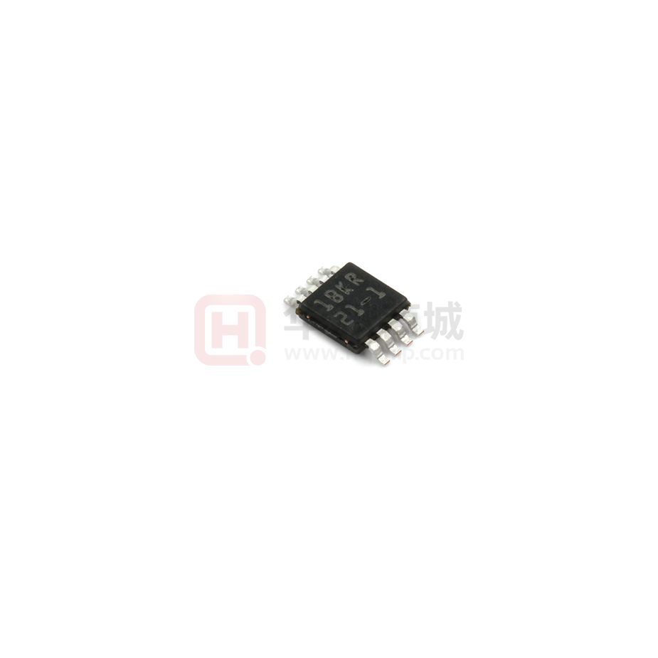
21-1
Samples
LM5021MM-2/NOPB
ACTIVE
VSSOP
DGK
8
1000
RoHS & Green
SN
Level-1-260C-UNLIM
-40 to 125
21-2
Samples
LM5021MMX-1/NOPB
ACTIVE
VSSOP
DGK
8
3500
RoHS & Green
SN
Level-1-260C-UNLIM
-40 to 125
21-1
Samples
LM5021MMX-2/NOPB
ACTIVE
VSSOP
DGK
8
3500
RoHS & Green
SN
Level-1-260C-UNLIM
-40 to 125
21-2
Samples
LM5021NA-1/NOPB
ACTIVE
PDIP
P
8
40
RoHS & Green
NIPDAU
Level-1-NA-UNLIM
-40 to 125
LM5021NA
-1
Samples
(1)
The marketing status values are defined as follows:
ACTIVE: Product device recommended for new designs.
LIFEBUY: TI has announced that the device will be discontinued, and a lifetime-buy period is in effect.
NRND: Not recommended for new designs. Device is in production to support existing customers, but TI does not recommend using this part in a new design.
PREVIEW: Device has been announced but is not in production. Samples may or may not be available.
OBSOLETE: TI has discontinued the production of the device.
(2)
RoHS: TI defines "RoHS" to mean semiconductor products that are compliant with the current EU RoHS requirements for all 10 RoHS substances, including the requirement that RoHS substance
do not exceed 0.1% by weight in homogeneous materials. Where designed to be soldered at high temperatures, "RoHS" products are suitable for use in specified lead-free processes. TI may
reference these types of products as "Pb-Free".
RoHS Exempt: TI defines "RoHS Exempt" to mean products that contain lead but are compliant with EU RoHS pursuant to a specific EU RoHS exemption.
Green: TI defines "Green" to mean the content of Chlorine (Cl) and Bromine (Br) based flame retardants meet JS709B low halogen requirements of


 工商网监
湘ICP备2023018690号
工商网监
湘ICP备2023018690号

