LM5027A
www.ti.com
SNVS642B – APRIL 2010 – REVISED MARCH 2013
Voltage Mode Active Clamp Controller
Check for Samples: LM5027A
FEATURES
DESCRIPTION
•
•
•
•
The LM5027A is a functional variant of the LM5027
active clamp PWM controller. The functional
difference of the LM5027A is that the maximum duty
cycle of the LM5027A is decreased from 91% to 71%.
In addition, the oscillator timing equation has been
modified.
1
2
•
•
•
•
•
•
•
•
•
Voltage-Mode Control
Line Feed-Forward PWM Ramp
Internal 105V Rated Start-Up Bias Regulator
Programmable Line Under-Voltage Lockout
(UVLO) with Adjustable Hysteresis
Versatile Dual Mode Over-Current Protection
Programmable Volt-Second Limiter and SoftStart
Programmable Synchronous Rectifier SoftStart and Stop
Precise 500mV Over-Current Comparator
Current Sense Leading Edge Blanking
Programmable Oscillator With 1 MHz
Maximum Frequency and Synchronization
Capability
Precision 5V Reference
Programmable Time Delays Between Outputs
A 70% Maximum Duty Cycle
The LM5027A pulse-width modulation (PWM)
controller contains all of the features necessary to
implement power converters utilizing the Active
Clamp / Reset technique. With the active clamp
technique, higher efficiencies and greater power
densities can be realized compared to conventional
catch winding or RDC clamp / reset techniques.
Three control outputs are provided: the main power
switch control (OUTA), the active clamp switch
control (OUTB), and secondary side synchronous
rectifier control (OUTSR). The timing between the
control outputs is adjustable with external resistors
that program internal precision timers. This controller
is designed for high-speed operation including an
oscillator frequency range up to 1 MHz and total
PWM propagation delays less than 50 ns. The
LM5027A includes a high-voltage startup regulator
with a maximum input voltage rating of 105V.
Additional features include Line Under Voltage
Lockout (UVLO), separate soft-start of main and
synchronous rectifier outputs, a timer for hiccup mode
current limiting, a precision reference, and thermal
shutdown.
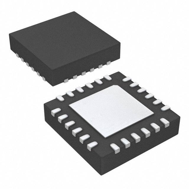
Packages
•
•
HTSSOP-20
WQFN-24
1
2
Please be aware that an important notice concerning availability, standard warranty, and use in critical applications of
Texas Instruments semiconductor products and disclaimers thereto appears at the end of this data sheet.
All trademarks are the property of their respective owners.
PRODUCTION DATA information is current as of publication date.
Products conform to specifications per the terms of the Texas
Instruments standard warranty. Production processing does not
necessarily include testing of all parameters.
Copyright © 2010–2013, Texas Instruments Incorporated
�LM5027A
SNVS642B – APRIL 2010 – REVISED MARCH 2013
www.ti.com
Typical Application Circuit
VIN
VOUT
CS
LM5027A
VCC
Vin
OUTA
RAMP
OUTB
UVLO
OUTSR
TIME3
COMP
REF
OTP
RT
TIME1
AGND
SSSR
ERROR AMP and
ISOLATION
TIME2
RES
SS
PGND
Figure 1. Simplified Active Clamp Converter
2
Submit Documentation Feedback
Copyright © 2010–2013, Texas Instruments Incorporated
Product Folder Links: LM5027A
�LM5027A
www.ti.com
SNVS642B – APRIL 2010 – REVISED MARCH 2013
4
17
RES
TIME1
5
16
SS
AGND
6
15
CS
RT
7
14
VCC
EP
COMP
8
13
PGND
REF
9
12
OUTSR
OUTB
10
11
OUTA
OTP
SSSR
TIME2
24
23
22
21
20
RAMP
1
19
SSSR
TIME 3
2
18
RES
TIME 2
3
17
SS
TIME 1
4
16
CS
AGND
5
15
VCC
RT
6
14
VCC
COMP
7
13
PGND
Figure 2. 20-Lead HTSSOP
EP
8
9
10
11
12
PGND
OTP
18
UVLO
19
OUTSR
2
3
NC
RAMP
TIME3
OUTA
UVLO
VIN
20
OUTB
1
REF
VIN
NC
Connection Diagram
Figure 3. 24-Lead WQFN
Table 1. Pin Descriptions
Pin
(1)
(1)
Name
Description
Application Information
Input voltage source
Input to the Start-up Regulator. Operating input range is 13V to 90V. The Absolute
Maximum Rating is 105V. For power sources outside of this range, the LM5027A
can be biased directly at VCC by an external regulator.
RAMP
Feed-forward modulation
ramp
An external RC circuit from VIN sets the PWM ramp slope. This pin is discharged
at the conclusion of every cycle by an internal FET. An internal comparator
terminates the PWM pulse if the RAMP pin exceeds 2.5V thus limiting the
maximum volt-second product to the transformer primary.
3
TIME3
Overlap delay 3
An external resistor sets the overlap delay for the active clamp output. The RTIME3
resistor connected between TIME3 and AGND sets the OUTA turn-off (falling
edge) to OUTB turn-on (falling edge) pulse delay. See Figure 26.
4
TIME2
Overlap delay 2
An external resistor sets the overlap delay for the OUTSR output. The RTIME2
resistor connected between TIME2 and AGND sets the OUTA turn-off (falling
edge) to OUTSR turn-on (rising edge) pulse delay. See Figure 26.
5
TIME1
Overlap delay 1
An external resistor sets the overlap delay for the active clamp output. The RTIME1
resistor connected between TIME1 and AGND sets the OUTB and OUTSR turnoff to OUTA turn-on pulse delay. See Figure 26.
6
AGND
Analog ground
Connect directly to Power Ground.
7
RT
Oscillator frequency control
and sync clock input
Normally biased at 2V by an internal amplifier. An external resistor connected
between RT and AGND sets the internal oscillator frequency. The internal
oscillator can be synchronized to an external clock with a frequency higher than
the free running frequency set by the RT resistor.
8
COMP
Input to the pulse width
modulator
An external opto-coupler connected to the COMP pin sources current into an
internal NPN current mirror. The PWM duty cycle is at its maximum value with
zero input current, while 1mA reduces the duty cycle to zero. The current mirror
improves the frequency response by reducing the ac voltage across the optocoupler detector transistor.
9
REF
Reference Output
Output of a 5V reference. Maximum output current is 10 mA. Locally decouple
with a 0.1 µF capacitor.
1
VIN
2
Note: The pin numbers shown are only for the HTSSOP package.
Submit Documentation Feedback
Copyright © 2010–2013, Texas Instruments Incorporated
Product Folder Links: LM5027A
3
�LM5027A
SNVS642B – APRIL 2010 – REVISED MARCH 2013
www.ti.com
Table 1. Pin Descriptions (continued)
Pin
4
(1)
Name
Description
Application Information
10
OUTB
Output driver
Control output of the active clamp PFET gate. Capable of 1A peak source and
sink current.
11
OUTA
Output driver
Control output of the main PWM NFET gate. Capable of 2A peak source and sink
current.
12
OUTSR
Output driver
Control output of the secondary side synchronous rectifier FET gates. Capable of
3A peak source and sink current.
13
PGND
Power ground
Connect directly to Analog Ground
14
VCC
Start-up regulator output
Output of the internal high voltage start-up regulator. Regulated at 9.5V during
start-up and 7.5V during run mode. If the auxiliary winding raises the voltage on
this pin above the regulation set point, the internal start-up regulator will
shutdown, thus reducing the IC power dissipation.
15
CS
Current sense input
Current sense input for cycle-by-cycle current limiting. If the CS pin exceeds
500mV the output pulse will be terminated, entering cycle-by-cycle current limit.
An internal switch holds CS low for 100 ns after OUTA switches high to blank
leading edge transients.
16
SS
Soft-start Input
An internal 22 µA current source charges an external capacitor to set the soft-start
rate.
17
RES
Restart timer
If cycle-by-cycle current limit is reached during any cycle, a 22 µA current is
sourced into the RES capacitor. If the RES capacitor voltage charges to 1.0V, a
hiccup sequence is initiated. The SS and SSSR capacitors are discharged and the
control outputs are disabled. The voltage on the RES capacitor is ramped
between 4V and 2V eight times. After the eighth cycle, the SS capacitor is
released and the normal start-up sequence begins.
18
SSSR
Soft-start for synchronous
rectifier output.
An external capacitor and an internal 25 µA current source sets the soft-start and
soft-stop ramps for the synchronous rectifier output (OUTSR).
19
OTP
Over-Temperature
Protection
The OTP comparator can be used for over-temperature shutdown protection with
an external NTC thermistor voltage divider setting the shutdown temperature. The
OTP comparator threshold is 1.25V. Hysteresis is set by an internal current
source that sources 20 µA into the external resistor divider when the OTP pin
voltage is above the threshold.
20
UVLO
Line under-voltage lockout
An external voltage divider from the power source sets the shutdown and standby
comparator levels. When UVLO reaches the 0.4V threshold, the VCC and REF
regulators are enabled. When UVLO reaches the 2.0V threshold, the SS pin is
released and the device enters the active mode. Hysteresis is set by an internal
current source that pulls 20 µA from the external resistor divider when the UVLO
pin is below the 2.0V threshold.
EP
Exposed pad, underside of
package
No electrical contact to the LM5027A integrated circuit. Connect to system ground
plane for reduced thermal resistance.
Submit Documentation Feedback
Copyright © 2010–2013, Texas Instruments Incorporated
Product Folder Links: LM5027A
�LM5027A
www.ti.com
SNVS642B – APRIL 2010 – REVISED MARCH 2013
These devices have limited built-in ESD protection. The leads should be shorted together or the device placed in conductive foam
during storage or handling to prevent electrostatic damage to the MOS gates.
Absolute Maximum Ratings (1) (2)
VIN to GND
-0.3V to 105V
VCC to GND
-0.3V to 16V
UVLO to GND
-0.3 to 8V
All other inputs to GND
-0.3 to 7V
COMP Input Current
COMP, REF
10 mA
(3)
ESD Rating, Human Body Model (4)
2kV
Storage Temperature Range
-55°C to 150°C
Junction Temperature
(1)
(2)
(3)
(4)
150°C
If Military/Aerospace specified devices are required, please contact the TI Sales Office/ Distributors for availability and specifications.
Absolute Maximum Ratings are limits beyond which damage to the device may occur. Operating Ratings are conditions under which
operation of the device is intended to be functional. For specifications and test conditions, see the Electrical Characteristics.
It is not recommended that external power sources be connected to these pins.
The human body model is a 100 pF capacitor discharged through a 1.5 kΩ resistor into each pin.
Operating Ratings (1)
VIN
13 to 90V
VCC
8 to 15V
Operating Junction Temperature
(1)
-40°C to +125°C
Absolute Maximum Ratings are limits beyond which damage to the device may occur. Operating Ratings are conditions under which
operation of the device is intended to be functional. For specifications and test conditions, see the Electrical Characteristics.
Electrical Characteristics
Limits in standard type are for TJ = 25°C only; limits in boldface type apply over the junction temperature range of –40°C to
+125°C. Unless otherwise specified, the following conditions apply: VIN = 48V, VCC = 10V, RT= 38.4K , No Load on OUTA,
OUTB and OUTSR unless otherwise stated.
Symbol
Parameter
Conditions
Min
Typ
Max
Units
6.8
mA
310
650
µA
9.9
VIN SUPPLY
Ibias
VIN Operating Current
COMP and VCC Open, UVLO and OTP = 3V
VIN Shutdown Current
UVLO = 0V, Vin = 100 V
VCC REGULATOR
VccReg
VCC Regulation
No Load (SS0.4V, VCC >9.5V
4.85
5.0
5.15
V
10
20
mV
10
17.5
3.8
Submit Documentation Feedback
Copyright © 2010–2013, Texas Instruments Incorporated
Product Folder Links: LM5027A
mA
V
5
�LM5027A
SNVS642B – APRIL 2010 – REVISED MARCH 2013
www.ti.com
Electrical Characteristics (continued)
Limits in standard type are for TJ = 25°C only; limits in boldface type apply over the junction temperature range of –40°C to
+125°C. Unless otherwise specified, the following conditions apply: VIN = 48V, VCC = 10V, RT= 38.4K , No Load on OUTA,
OUTB and OUTSR unless otherwise stated.
Symbol
Parameter
Conditions
Min
Typ
Max
Units
1.9
2
2.1
V
20
25
µA
UVLO/OTP THRESHOLDS
UVLO Threshold
UVLO Hysteresis Current
UVLO
UVLO Shutdown Threshold
ULVLO voltage falling
16
0.3
V
UVLO Standby Enable Threshold
UVLO voltage rising
0.4
V
OTP Shutdown Threshold
OTP rising
1.21
1.25
1.29
V
OTP Hysteresis Current
OTP
15
20
24
µA
SS Charging Current Source
SS = 0V
17
22
26
µA
3.85
4.05
4.25
V
18
25
30
µA
SSSR Discharge Current Source
in Soft Stop
14
20
26
µA
SSSR Falling Threshold for SS
Soft Stop
1.5
2.2
3.0
V
SOFT-START
SS Rising Threshold for SSSR
charge current enable
SSSR Charging Current Source
SS output low voltage
SSSR = 0V, SS>4V
Sinking 100 µA UVLO = 0
SSSR output low voltage
120
mV
100
mV
OSCILLATOR
Frequency1
RT = 38.4 kΩ
275
Sync Threshold
310
345
kHz
150
ns
2.85
Sync Pulse Width
15
V
PWM COMPARATORS
Delay to Output
50
COMP to PWM Offset
1.0
Duty Cycle Maximum
OUTA, OUT_A = Tdelay_min
70
72.5
ns
V
75
%
22
26
µA
CURRENT LIMIT RESTART (RES Pin)
RES Threshold
1.1
V
Charge Source Current Level 1
VRES < 1.0V
Charge Source Current Level 2
4.0V < VRES > 1.0V
4
5.0
6.5
µA
Discharge Current Source
VRES ramping down
4
5
7
µA
Ratio of RES Threshold to SS
Low
VRES > 1V, Hiccup counter
550
mV
125
CURRENT LIMIT
CS prop
Cycle by cycle sense voltage
threshold
RAMP = 0
450
500
Current limit propagation delay
CS step from 0 to 0.6V time to onset of OUTA
transition (90%) Cgate = 0pen
30
ns
RDS(ON)
5
Ω
VOLTAGE FEED-FORWARD (RAMP Pin)
RAMP Discharge Device
VOLT-SECOND CLAMP
Ramp Clamp Level
6
Delta RAMP measured from onset of OUTA to
Ramp peak. Comp = 5V
Submit Documentation Feedback
2.3
2.5
2.6
V
Copyright © 2010–2013, Texas Instruments Incorporated
Product Folder Links: LM5027A
�LM5027A
www.ti.com
SNVS642B – APRIL 2010 – REVISED MARCH 2013
Electrical Characteristics (continued)
Limits in standard type are for TJ = 25°C only; limits in boldface type apply over the junction temperature range of –40°C to
+125°C. Unless otherwise specified, the following conditions apply: VIN = 48V, VCC = 10V, RT= 38.4K , No Load on OUTA,
OUTB and OUTSR unless otherwise stated.
Symbol
Parameter
Conditions
Min
Typ
Max
Units
0.15
0.5
V
OUTA GATE DRIVER
VOL
OUTA Low-state Output Voltage
IOUTA = 100 mA
VOH
OUTA High-state Output Voltage
IOUTA = -100 mA, VOHL = VCC -VLO
0.21
V
OUTA Rise Time
C-load = 1000 pF
10
ns
OUTA Fall Time
C-load = 1000 pF
13
ns
IOHL
Peak OUTA Source Current
VOUTA = 0V (VCC = 10V)
2
A
IOLL
Peak OUTA Sink Current
VOUTA = VCC= 10V
2
A
0.35
OUTB GATE DRIVER
VOL
OUTB Low-state Output Voltage
IOUTB = 100 mA
0.2
VOH
OUTB High-state Output Voltage
IOUTB = -100 mA, VOHL = VCC -VLO
0.31
V
OUTB Rise Time
C-load = 1000 pF
15
ns
OUTB High Side Fall Time
C-load = 1000 pF
13
ns
IOHL
Peak OUTB Source Current
VOUTB = 0V (VCC = 10V)
1
A
IOLL
Peak OUTB Sink Current
VOUTB = VCC= 10V
1
A
0.5
0.4
V
OUTSR GATE DRIVER
VOL
OUTSR Low-state Output Voltage IOUTSR = 100 mA
VOH
OUTSR High-state Output
Voltage
IOUTSR = -100 mA, VOHL = VCC -VLO
OUTSR Rise Time
0.1
0.25
0.2
V
0.11
V
C-load = 1000 pF
12
ns
OUTSR High Side Fall Time
C-load = 1000 pF
10
ns
IOHH
Peak OUTSR Source Current
VOUTSR = 0V (VCC = 10V)
3
A
IOLH
Peak OUTSR Sink Current
VOUTSR = VCC= 10V
3
A
OUTPUT TIMING CONTROL
T1
Delay Leading Range
RTIME1=10 kΩ – 100 kΩ
30
T1
Delay Leading Accuracy
RTIME1 = 33.2 kΩ
75
T2
Delay Trailing Range
RTIME2 = 10 kΩ – 100 kΩ
30
T2
Delay Trailing Accuracy
RTIME2 = 28.7 kΩ
75
T3
Delay Leading Range
RTIME3 = 10 kΩ – 100 kΩ
30
T3
Delay Leading Accuracy
RTIME3 = 29.4 kΩ
75
100
150
100
100
300
ns
125
ns
300
ns
125
ns
300
ns
125
ns
THERMAL
tsd
Thermal Shutdown Temp.
165
°C
Thermal Shutdown Hysteresis
25
°C
RJA
Junction to Ambient
40
°C/W
RJC
Junction to Exposed Pad
4
°C/W
Submit Documentation Feedback
Copyright © 2010–2013, Texas Instruments Incorporated
Product Folder Links: LM5027A
7
�LM5027A
SNVS642B – APRIL 2010 – REVISED MARCH 2013
www.ti.com
Typical Performance Characteristics
Efficiency
VCC and VREF vs. VIN
Figure 4.
Figure .
VCC vs. ICC
VREF vs. IREF
6
5
VREF (V)
4
3
2
1
0
0
5
10
15
20
IREF (mA)
8
Figure 5.
Figure 6.
Oscillator Frequency vs RT Resistor
Oscillator Frequency vs Temperature
Figure 7.
Figure 8.
Submit Documentation Feedback
Copyright © 2010–2013, Texas Instruments Incorporated
Product Folder Links: LM5027A
�LM5027A
www.ti.com
SNVS642B – APRIL 2010 – REVISED MARCH 2013
Typical Performance Characteristics (continued)
Time1 Delay vs RTIME1 (kΩ)
Time2 Delay vs RTIME2 (kΩ)
Figure 9.
Figure 10.
Time3 Delay vs RTIME3 (kΩ)
Time1 Delay vs Temperature
RTIME1 = 33.2 kΩ
Figure 11.
Figure 12.
Time2 Delay vs Temperature
RTIME2 = 28.7 kΩ
Time3 Delay vs Temperature
RTIME3 = 29.4 kΩ
Figure 13.
Figure 14.
Submit Documentation Feedback
Copyright © 2010–2013, Texas Instruments Incorporated
Product Folder Links: LM5027A
9
�LM5027A
SNVS642B – APRIL 2010 – REVISED MARCH 2013
www.ti.com
Typical Performance Characteristics (continued)
SS Pin Current vs Temperature
SSSR Pin Charging Current vs Temperature
Figure 15.
Figure 16.
RES Pin Charging Current Level 1 vs Temperature
Figure 17.
10
Submit Documentation Feedback
Copyright © 2010–2013, Texas Instruments Incorporated
Product Folder Links: LM5027A
�LM5027A
www.ti.com
SNVS642B – APRIL 2010 – REVISED MARCH 2013
BLOCK DIAGRAM
9.5V-7.7 V
REGULATOR
VIN
VCC
+
1.25V
OTP
VCC
UVLO
5.0V
+
0.4V
UVLO
REF
OTP HYSTERESIS (20 uA)
SHUTDOWN
-
LOGIC
TIME1
THERMAL
LIMIT
+
2.0V
5V
REFERENCE
TIME 2
STANDBY
-
TIME 3
UVLO HYSTERESIS (20 uA)
S
Q
CLK
DRIVER
RT
OUTA
R
OSCILLATOR
OVERLAP
AND DRIVE
DELAY
DRIVER
OUTB
RAMP
FF
RAMP
REF
DRIVER
25 uA
2.5V Max V*S Clamp
2.5V
SSSR
+
-
LOGIC
20 uA
Soft-Stop
REF
5V
5k
OUTSR
1V
COMP
SS
PWM
22 uA
+
-
SS
SS
REF
1:1
CS
0.50V
CS
-
5 uA
REF
RESTART
TIMER
LOGIC AND
DIVIDE-BY- 8
COUNTER
+
CLK + LEB
22 uA
RES
PGND
5 uA
+
AGND
-
1.0V
Figure 18. Simplified Block Diagram
Submit Documentation Feedback
Copyright © 2010–2013, Texas Instruments Incorporated
Product Folder Links: LM5027A
11
�LM5027A
SNVS642B – APRIL 2010 – REVISED MARCH 2013
www.ti.com
DETAILED OPERATING DESCRIPTION
The LM5027A PWM controller contains all the features necessary to implement power converters utilizing the
Active Clamp Reset technique with synchronous rectification. The device is configured to control a P-Channel
clamp switch. With the active clamp technique higher efficiencies and greater power densities can be realized
compared to conventional catch winding or RDC clamp / reset techniques. The LM5027A provides three gate
driver outputs: one to drive the primary side MOSFET (OUTA), one for the active clamp P-Channel MOSFET
(OUTB), and one output to drive the synchronous rectifier through an isolation interface (OUTSR). This controller
is designed for high-speed operation including an oscillator frequency range up to 1 MHz and total PWM and
current sense propagation delay less than 50 ns. The LM5027A includes a high-voltage start-up regulator that
operates over a wide input range of 13V to 90V. Additional features include: Line Under-Voltage lockout (UVLO),
soft-start/soft-stop, oscillator with synchronization capability, cycle-by-cycle current limit, hiccup mode fault
protection with adjustable delay, precision reference, and thermal shutdown.
High Voltage Start-Up Regulator
The LM5027A contains an internal high voltage start-up regulator that allows the input pin (VIN) to be connected
directly to the line voltage. The regulator output is internally current limited to 55mA. When the UVLO pin
potential is greater than 0.4V, the VCC regulator is enabled to charge an external capacitor connected to the
VCC pin. The VCC regulator provides power to the voltage reference (REF) and the gate drivers (OUTA, OUTB,
and OUTSR). The controller outputs are enabled when the voltage on the VCC pin reaches the regulation point
of 9.5V, the internal voltage reference (REF) reaches its regulation point of 5V, the UVLO pin voltage is greater
than 2V, and the OTP pin voltage is greater than 1.25V. The outputs will remain enabled unless one of the
following conditions occurs, VCC falls below 6.0V, UVLO is below 2.0 V, or the OTP pin falls below 1.25V. The
value selected for the VCC capacitor depends on the total system design and the start-up characteristics. The
recommended capacitance range for the VCC regulator is 0.1 µF to 100 µF. In a typical application, an auxiliary
transformer winding is connected through a diode to the VCC pin. This winding must raise the VCC voltage
above the VCC regulation set point to shut off the internal start-up regulator. The LM5027A lowers the VCC
regulation set point from 9.5V to 7.5V after the output of the first OUTSR drive pulse. Powering VCC from an
auxiliary winding improves efficiency while reducing the controller power dissipation. When the converter auxiliary
winding is inactive, external current draw on the VCC line should be limited so the power dissipation in the startup regulator does not exceed the maximum power dissipation of the LM5027A package. An external start-up
regulator or other bias rail can be used instead of the internal start-up regulator by connecting the VCC and the
VIN pins together and feeding the external bias into the two pins.
Line Under-Voltage Detector
The LM5027A contains a dual level line Under Voltage Lock Out (UVLO) circuit. When the UVLO pin voltage is
greater than 0.4V but less than 2.0V, the controller is in a standby mode. In the standby mode the VCC and REF
bias regulators are active while the controller outputs are disabled. This feature allows the UVLO pin to be used
as a remote enable/disable function. Pulling the UVLO pin below the 2.0V threshold initiates a soft-stop
sequence described later in this document. There is 100mV of hysteresis provided in the 0.4V shutdown
comparator. When the VCC and REF outputs exceed their respective under-voltage thresholds and the UVLO
pin voltage is greater than 2.0V and the OTP pin voltage is greater than 1.25V, the outputs are enabled and
normal operation begins. An external set-point voltage divider from the VIN to GND can be used to set the
minimum operating voltage of the converter. The divider must be designed such that the voltage at the UVLO pin
will be greater than 2.0V when Vin is in the desired operating range. If the under-voltage threshold is not met, all
three outputs are disabled. UVLO hysteresis is accomplished with an internal 20 µA current sink that is switched
on or off into the impedance of the set-point divider. When the UVLO pin voltage exceeds 2.0V threshold, the
current sink is deactivated to quickly raise the voltage at the UVLO pin. When the UVLO pin voltage falls below
the 2.0V threshold, the current sink is turned on causing the voltage at the UVLO pin to quickly fall .
Reference
The REF pin is the output of a 5V linear regulator that can be used to bias an opto-coupler transistor and
external house-keeping circuits. The regulator output is internally current limited to 10 mA.
12
Submit Documentation Feedback
Copyright © 2010–2013, Texas Instruments Incorporated
Product Folder Links: LM5027A
�LM5027A
www.ti.com
SNVS642B – APRIL 2010 – REVISED MARCH 2013
Cycle-by-Cycle Current Limit
The CS pin is to be driven by a signal representative of the transformer primary current. If the voltage on the CS
pin exceeds 0.5V, the current sense comparator terminates the output driver pulse, with the duty cycle
determined by the current sense comparator instead of the PWM comparator. A small R-C filter connected to the
CS pin and located near the controller is recommended to suppress noise. An internal 5Ω MOSFET discharges
the external current sense filter capacitor at the conclusion of every cycle. The discharge MOSFET remains on
for an additional 30 ns after either OUTA driver switches high to blank leading edge transients in the current
sensing circuit. Discharging the CS pin filter each cycle and blanking leading edge spikes reduces the filtering
requirements and improves the current sense response time. The current sense comparator is very fast and may
respond to short duration noise pulses. Layout considerations are critical for the current sense filter and sense
resistor. The capacitor associated with the CS filter must be placed very close to the device and connected
directly to the CS and AGND pins. If a current sense transformer is used, both leads of the transformer
secondary should be routed to the filter network, which should be located close to the IC. When designing with a
current sense resistor, all of the noise sensitive low power ground connections should be connected together
near the AGND pin, and a single connection should be made to the power ground (sense resistor ground point).
Restart Time Delay (Hiccup Mode)
The LM5027A provides a current limit restart timer to disable the outputs and force a delayed restart (hiccup
mode) if a current limit condition is repeatedly sensed. The number of cycle-by-cycle current limit events required
to trigger the restart is programmable by the external capacitor at the RES pin. During each PWM cycle, the
LM5027A either sources or sinks current from the RES pin capacitor. If no current limit is detected during a cycle,
a 5 µA current sink is enabled to pull the RES pin to ground. If a current limit is detected, the 5 µA current sink is
disabled and a 22 µA current source causes the voltage at the RES pin to gradually increase. If the RES voltage
reaches the 1.0V threshold, the following restart sequence occurs (also see Figure 19).
• The SS and SSSR capacitors are fully discharged.
• The RES 20 µA current source is turned-off and the 5 µA current source is turned-on.
• The voltage on the RES pin is allowed to charge up to 4.0V.
• When voltage on the RES pin reaches 4.0V the 5 µA current source is turned-off and a 5 µA current sink is
turned-on, ramping the voltage on the RES capacitor down to 2.0V.
• The RES capacitor voltage is ramped between 4.0V and 2.0V eight times.
• When the counter reaches eight, the RES pin voltage is pulled low and the Soft-Start capacitor is released to
begin a soft-start sequence. The SS capacitor voltage slowly increases. When the SS voltage reaches 1.0V, the
PWM comparator will produce the first narrow output pulse at OUTA.
• When the SS voltage reaches 4.0V the capacitor on the SSSR pin is released and is charged with a 25 µA
current source, soft-starting the free-wheeling synchronous rectifier.
• If the overload condition persists after restart, cycle-by-cycle current limiting will begin to increase the voltage
on the RES capacitor again, repeating the hiccup mode sequence.
• If the overload condition no longer exists after restart, the RES pin will be held at ground by the 5 µA current
sink and normal operation resumes.
Submit Documentation Feedback
Copyright © 2010–2013, Texas Instruments Incorporated
Product Folder Links: LM5027A
13
�LM5027A
SNVS642B – APRIL 2010 – REVISED MARCH 2013
www.ti.com
CS Limit
Threshold
4.0 V
2.0V
1.0 V
RES
Divide - by - eight
counter
Restart delay
4.0 V
Soft - Start
1.0 V
Hiccup Mode
off - time
SSSR
SSSR
Figure 19. Restart and Soft-Start Delay Timing
Soft-Start
The soft-start circuit allows the regulator to gradually increase its output voltage until the steady state operating
point is reached; thereby reducing start-up stresses and surge currents. When bias power is supplied to the
LM5027A, the SS pin capacitor is discharged by an internal MOSFET. When the voltages on the UVLO, OTP,
VCC, and REF pins reach the operating thresholds, the soft-start capacitor is released and is charged with a 22
µA current source. When the SS pin voltage reaches 1V, output pulses commence with a slowly increasing duty
cycle (refer to Figure 20, Figure 21 and Figure 22). The voltage on the SS pin eventually increases to 5V, while
the voltage at the PWM comparator is limited to the level required for regulation as determined by the voltage
feedback loop via the COMP pin. When the soft-start voltage reaches 4.0V, the capacitor on the SSSR pin is
released and charged with a 25 µA current source (refer to Figure 20, Figure 21 and Figure 22) . When the
SSSR pin voltage reaches approximately 2.5V (refer to Figure 23), the internal synchronous rectifier PWM circuit
gradually increases the synchronous rectifier drive duty cycle (OUTSR) in proportion the rising SSSR pin voltage.
Delaying the start of the SSSR gate drive pulses until after the main soft-start is completed allows the output
voltage to reach regulation before the synchronous rectifiers begins operation. This delay prevents the
synchronous rectifier from sinking current from the output in applications where the output voltage may be prebiased.
14
Submit Documentation Feedback
Copyright © 2010–2013, Texas Instruments Incorporated
Product Folder Links: LM5027A
�LM5027A
www.ti.com
SNVS642B – APRIL 2010 – REVISED MARCH 2013
Soft-Stop
If the UVLO pin voltage falls below the 2.0V standby threshold, but above the 0.4V shutdown threshold, the
synchronous rectification soft-start capacitor is discharged with a 20 µA current source which gradually disables
the synchronous rectifiers (refer to Figure 21). After the SSSR capacitor has been discharged to 2.0V the softstart and synchronous rectification soft-start capacitors are quickly discharged to ground to terminate PWM
pulses at OUTA ,OUTB, and OUTSR. The PWM pulses may cease before the SSSR voltage reduces the
synchronous rectifier duty cycle if the VCC or REF voltage drops below the respective under-voltage thresholds
during the soft-stop process. This soft-stop method of turning off the converter prevents oscillations in the
synchronous rectifiers during a shutdown sequence.
increasing PWM
SS pulse width
PWM
increasing OUTA
SS pulse width
OUTA
OUTB
increasing SR SS pulse width
SR
Figure 20. Soft-Start Timing
Submit Documentation Feedback
Copyright © 2010–2013, Texas Instruments Incorporated
Product Folder Links: LM5027A
15
�LM5027A
SNVS642B – APRIL 2010 – REVISED MARCH 2013
UVLO < 2V
www.ti.com
UVLO > 2V
0.4V < UVLO < 2V
UVLO
5V
SS
~3V
1V
OUTA, OUTB
Soft-Start
4.5V
5V
4.5V
2.5V
2V
2.5V
SSSR
OUTSR
Soft-Stop
OUTSR
Soft-Start
Figure 21. Soft-Start/Soft-Stop Timing
UVLO > 2.0V
UVLO
SS
~1V
Expanded view
Soft -Start
SSSR
OUTA
OUTB
OUTSR
Figure 22. Soft-Start and Drive Enable
16
Submit Documentation Feedback
Copyright © 2010–2013, Texas Instruments Incorporated
Product Folder Links: LM5027A
�LM5027A
www.ti.com
SNVS642B – APRIL 2010 – REVISED MARCH 2013
UVLO > 2.0V
UVLO
~ 4V
SS
Expanded view
SR
Soft -Start
~1V
SSSR
~2.5V
OUTA
OUTB
OUTSR
Figure 23. Soft-Start Synchronous Rectifier Timing
External Over-Temperature Protection
An external set-point voltage divider between the REF, OTP, and AGND pins, as shown in Figure 24, is one
method to implement over-temperature protection shutdown. Typically a NTC thermistor is installed as the lower
device of the voltage divider. The divider must be designed such that the voltage at the OTP pin will be greater
than 1.25V when there is not an over-temperature condition, and the OTP pin must drop below 1.25V during an
over-temperature event. OTP hysteresis is accomplished with an internal 20 µA current source that is switched
on or off into the impedance of the external set-point divider. When the OTP pin voltage exceeds 1.25V
threshold, the current source is activated to quickly raise the voltage at the OTP pin. When the OTP pin voltage
falls below the 1.25V threshold, the current source is turned off causing the voltage at the OTP pin to quickly fall.
When OTP falls below 1.25V the LM5027A will go through a soft-stop turn-off sequence.
REF
RTOP
1.25V
OTP
+
Logic
5.0V
NTC
OTP HYSTERESIS (20 uA)
LM5027A
Figure 24. External OTP Protection
Submit Documentation Feedback
Copyright © 2010–2013, Texas Instruments Incorporated
Product Folder Links: LM5027A
17
�LM5027A
SNVS642B – APRIL 2010 – REVISED MARCH 2013
www.ti.com
Fault/Events Summary
Table 2 is a Truth Table which describes the faults and events that control the LM5027A drive outputs. For
example the first event is with UVLO being pulled below 0.4V, a possible remote shutdown condition. When this
occurs the SS, and SSSR capacitors are discharged, and the three drive outputs will stop switching (outputs
low). The last fault is if the OTP pin is pulled low 1.25V
Fast discharge
Fast
discharge
Low
Low
Low
2.0V0.4V
>6.2V
-
>1.25V
Fast discharge
after SSSR2.0V
>1.25V
-
Fast
discharge
Low
Low
Low
SSSR6.2V
>2.0V
>1.25V
>4.0V
-
Switching
Switching
Low
OTP6.2V
>2.0V
-
Fast discharge
after SSSR 100V
For applications where the system input voltage (VPWR) exceeds 100V, VIN can be powered from an external
start-up regulator as shown in Figure 28. Connecting the VIN and VCC pins together allows the LM5027A to be
operated with VIN below 13V. To turn-off the internal start-up regulator the VCC voltage must be raised above
9.9V. The voltage at the VCC pin must not exceed 15V. The voltage source at the right side of Figure 28 is
typically derived from the power stage, and becomes active when the LM5027A outputs are active.
VPWR
VIN
VCC
LM5027A
10V-15V (from
power stage)
10V
Figure 28. Start-up Regulator for VPWR > 100V
UVLO
The under-voltage lockout threshold (UVLO) is internally set to 2.0V at the UVLO pin. With two external resistors
as shown in Figure 29, the LM5027A is enabled when VPWR causes the UVLO pin to exceed threshold voltage of
2V. When VPWR is below the threshold, the internal 20 µA current sink is enabled to reduce the voltage at the
UVLO pin. When the UVLO pin voltage exceeds the 2V threshold, the 20 µA current sink is turned off causing
the UVLO voltage to increase and providing hysteresis. The values of R1 and R2 can be determined from the
following equation:
R1 = VHYS/20 µA
(5)
2.0 x R1
R2 =
VPWR - 2.0 - 20 PA x R1
(6)
Where VHYS is the desired UVLO hysteresis at VPWR, and VPWR in the second equation is the turn-on voltage. For
example, if the LM5027A is to be enabled when VPWR reaches 34V, and the hysteresis is 1.8V, then R1 is 90 kΩ
and 5.6 kΩ. For this application R1 was selected to be 90.0 kΩ, R2 was selected to be 6.19 kΩ. The LM5027A
can be remotely shutdown by taking the UVLO pin below 0.4V with an external open collector or open drain
device, as shown in Figure 29. The outputs and the VCC regulator are disabled in shutdown mode.
22
Submit Documentation Feedback
Copyright © 2010–2013, Texas Instruments Incorporated
Product Folder Links: LM5027A
�LM5027A
www.ti.com
SNVS642B – APRIL 2010 – REVISED MARCH 2013
VPWR
LM5027A
R1
20 PA
UVLO
+
2V
ON/OFF
control
R2
Figure 29. UVLO Circuit with Shutdown Control
Oscillator
The oscillator frequency is generally selected in conjunction with the system magnetic components and any other
aspects of the system which may be affected by the frequency. The RT resistor selection equation is specified in
the Oscillator and Sync Capability section. If the required frequency tolerance is critical in particular application,
the tolerance of the external resistor and the frequency tolerance specified in the Electrical Characteristics table
must be considered when selecting the RT resistor.
Voltage Feedback
The COMP pin is designed to accept a current input typically from an opto-coupler. A typical configuration is
shown in Figure 30, where the emitter of the opto-coupler transistor is connected to the COMP pin and the
collector is connected to the REF pin of the LM5027A. When the output voltage is below regulation, no current
flows into the COMP pin and the LM5027A operates at maximum duty cycle. At the secondary side, VOUT is
compared to a reference by the error amplifier which has an appropriate frequency compensation network. The
amplifier output drives the opto-coupler, which in turn drives the LM5027A COMP pin current mirror.
+VOUT
+SB
LM5027A
REF
5V
5k
+SB
COMP
Feedback
Optocoupler
PWM
Comparator
Error
Amplifier
VREF
1:1
Figure 30. Typical COMP Configuration
Submit Documentation Feedback
Copyright © 2010–2013, Texas Instruments Incorporated
Product Folder Links: LM5027A
23
�LM5027A
SNVS642B – APRIL 2010 – REVISED MARCH 2013
www.ti.com
Current Sense
The CS pin receives an input signal representative of the transformer primary current, either from a current sense
transformer or from a resistor in series with the source of the primary switch, as shown in Figure 31 and
Figure 32. In both cases the sensed current creates a ramping voltage across RSENSE, and the RF/CF filter
suppresses noise and leading edge transients. The filtering components RSENSE, RF and CF should be
physically as close to the LM5027A as possible. The current sense components must be scaled for 0.5V at the
CS pin when an over-current condition exists.
If the voltage on the CS pin reaches 0.5V, the present cycle will be immediately terminated. If the over-load event
continues and the RES pin reaches 1V, the soft-start capacitor is discharged and the LM5027A will go through
an auto re-start (Hiccup Mode). The Hiccup Mode time is set by the capacitor on the RES pin.
V PWR
Current
Sense
RF
CF
CS
Rsense
LM5027A
OUTA
OUTB
OUTSR
Figure 31. Transformer Current Sense
24
Submit Documentation Feedback
Copyright © 2010–2013, Texas Instruments Incorporated
Product Folder Links: LM5027A
�LM5027A
www.ti.com
SNVS642B – APRIL 2010 – REVISED MARCH 2013
VOUT
VPWR
OUTA
CS
RF
Rsense
CF
LM5027A
OUTB
OUTSR
Figure 32. Resistor Current Sense
Soft-Start
The capacitor on the SS pin determines the time required for the output duty cycle to increase from zero to its
final value for regulation. The minimum acceptable time is dependent on the output capacitance and the
response of the feedback loop that controls the COMP pin. If the soft-start time is too quick, the output could
significantly overshoot its intended voltage before the feedback loop has a chance to regulate the PWM
controller. After power is applied and VCC has passed its upper UV threshold (9.5V), the voltage at the SS pin
ramps up as the external capacitor is charged with an internal 20 μA current source. The voltage at the internal
PWM comparator input node follows the voltage at the SS pin. When the voltage on the SS pin has reached
1.0V, PWM pulses appear at the drive output with a very low duty cycle. The voltage at the SS pin eventually
increases to approximately 5.0V. The voltage at the input to the PWM comparator and the PWM duty cycle
increase to the value required for regulation as determined by the voltage regulation loop.
Hiccup Mode Current Limit Restart
Hiccup mode operation is described in the Restart Time Delay (Hiccup Mode) section. In the case of continuous
current limit detection at the CS pin, the time required to reach the 1.0V RES pin threshold is:
CRES x 1.0V
tCS =
22 PA
(7)
For example, if CRES = 0.047 µF the time tCS in Figure 33 is approximately 2.14 ms. After the voltage on the RES
pin reaches 1.0V, the 22 µA current source is turned-off and a 5 µA current source is turned-on. The Hiccup
Mode time is:
thiccup =
(4.0 - 1.0)CRES
'V x CRES
x8
+
5 PA
5 PA
(8)
where ΔV is 2.0V. With a CRES = 0.047 µF, the Hiccup Mode time is 179 ms. After the Hiccup Mode off time is
complete, the RES pin voltage is pulled low and soft-start capacitor is released allowing a soft-start sequence to
commence.
Submit Documentation Feedback
Copyright © 2010–2013, Texas Instruments Incorporated
Product Folder Links: LM5027A
25
�LM5027A
SNVS642B – APRIL 2010 – REVISED MARCH 2013
www.ti.com
The soft-start time trestart is set by the internal 22 µA current source, and is equal to:
CSS x 3.0V
trestart =
22 PA
(9)
If CSS = 0.1 µF, trestart is = 6.41 ms
The hiccup mode provides the periodic cool-down time for the power converter in the event of a sustained
overload or short circuit. This off time results in lower average input current and lower power dissipation within
the power components.
CS Limit
Threshold
4.0 V
2.0V
1.0 V
Divide - by - eight
counter
RES
tcs
3.0 V
Soft - Start
1.0 V
thiccup
trestart
Figure 33. Hiccup Mode Timing
Printed Circuit Board Layout
The LM5027A Current Sense and PWM comparators are very fast and respond to short duration noise pulses.
The components at the CS, COMP, SS, UVLO, TIME1, TIME2, and TIME3 pins should be physically close as
possible to the IC, thereby minimizing noise pickup on the PC board trace inductance. Layout consideration is
critical for the current sense filter. If a current sense transformer is used, both leads of the transformer secondary
should be routed to the sense filter components and to the IC pins. The ground side of the transformer should be
connected via a dedicated PC board trace to the AGND pin, rather than through the ground plane.
If the current sense circuit employs a sense resistor in the drive transistor source, low inductance resistors
should be used. In this case, all the noise sensitive, low-current ground trace should be connected in common
near the IC, and then a single connection made to the power ground (sense resistor ground point). The gate
drive outputs of the LM5027A should have short, direct paths to the power MOSFETs in order to minimize
inductance in the PC board. The two ground pins (AGND, PGND) must be connected together with a short,
direct connection, to avoid jitter due to relative ground bounce.
26
Submit Documentation Feedback
Copyright © 2010–2013, Texas Instruments Incorporated
Product Folder Links: LM5027A
�LM5027A
www.ti.com
SNVS642B – APRIL 2010 – REVISED MARCH 2013
Application Circuit Example
The following schematic shows an example of the LM5027A controlling a 100W active clamp forward power
converter. The input voltage range (VPWR) is 36V to 76V, and the output voltage is 3.3V. The output current
capability is 30 Amps. Current sense transformer T3 provides information to the CS pin for current limit
protection. The error amplifier and reference U3 and U5 provide voltage feedback via opto-coupler U2.
Synchronous rectifiers Q3-Q6 minimize rectification losses in the secondary. An auxiliary winding on the power
transformer T1 provides power to the LM5027A VCC pin when the output is in regulation. The input UVLO levels
are 34V for increasing VPWR, and approximately 32V for decreasing VPWR. The circuit can be shutdown by forcing
the ON/OFF input J2 below 0.4V. An external synchronizing frequency can be applied to the Oscillator input. The
converter output current limit is limited at 32A.
Special care was taken in this design such that the converter will turn on with the output pre-biased without
sinking current from the output. More information is available in TBD.
Figure 34. Application Circuit
Submit Documentation Feedback
Copyright © 2010–2013, Texas Instruments Incorporated
Product Folder Links: LM5027A
27
�LM5027A
SNVS642B – APRIL 2010 – REVISED MARCH 2013
www.ti.com
REVISION HISTORY
Changes from Revision A (March 2013) to Revision B
•
28
Page
Changed layout of National Data Sheet to TI format .......................................................................................................... 27
Submit Documentation Feedback
Copyright © 2010–2013, Texas Instruments Incorporated
Product Folder Links: LM5027A
�PACKAGE OPTION ADDENDUM
www.ti.com
11-Apr-2013
PACKAGING INFORMATION
Orderable Device
Status
(1)
Package Type Package Pins Package
Drawing
Qty
Eco Plan
Lead/Ball Finish
(2)
MSL Peak Temp
Op Temp (°C)
Top-Side Markings
(3)
(4)
LM5027AMH/NOPB
ACTIVE
HTSSOP
PWP
20
73
Green (RoHS
& no Sb/Br)
CU SN
Level-1-260C-UNLIM
-40 to 125
LM5027A
MH
LM5027AMHX/NOPB
ACTIVE
HTSSOP
PWP
20
2500
Green (RoHS
& no Sb/Br)
CU SN
Level-1-260C-UNLIM
-40 to 125
LM5027A
MH
LM5027ASQ/NOPB
ACTIVE
WQFN
NHZ
24
1000
Green (RoHS
& no Sb/Br)
CU SN
Level-1-260C-UNLIM
-40 to 125
L5027A
LM5027ASQX/NOPB
ACTIVE
WQFN
NHZ
24
4500
Green (RoHS
& no Sb/Br)
CU SN
Level-1-260C-UNLIM
-40 to 125
L5027A
(1)
The marketing status values are defined as follows:
ACTIVE: Product device recommended for new designs.
LIFEBUY: TI has announced that the device will be discontinued, and a lifetime-buy period is in effect.
NRND: Not recommended for new designs. Device is in production to support existing customers, but TI does not recommend using this part in a new design.
PREVIEW: Device has been announced but is not in production. Samples may or may not be available.
OBSOLETE: TI has discontinued the production of the device.
(2)
Eco Plan - The planned eco-friendly classification: Pb-Free (RoHS), Pb-Free (RoHS Exempt), or Green (RoHS & no Sb/Br) - please check http://www.ti.com/productcontent for the latest availability
information and additional product content details.
TBD: The Pb-Free/Green conversion plan has not been defined.
Pb-Free (RoHS): TI's terms "Lead-Free" or "Pb-Free" mean semiconductor products that are compatible with the current RoHS requirements for all 6 substances, including the requirement that
lead not exceed 0.1% by weight in homogeneous materials. Where designed to be soldered at high temperatures, TI Pb-Free products are suitable for use in specified lead-free processes.
Pb-Free (RoHS Exempt): This component has a RoHS exemption for either 1) lead-based flip-chip solder bumps used between the die and package, or 2) lead-based die adhesive used between
the die and leadframe. The component is otherwise considered Pb-Free (RoHS compatible) as defined above.
Green (RoHS & no Sb/Br): TI defines "Green" to mean Pb-Free (RoHS compatible), and free of Bromine (Br) and Antimony (Sb) based flame retardants (Br or Sb do not exceed 0.1% by weight
in homogeneous material)
(3)
MSL, Peak Temp. -- The Moisture Sensitivity Level rating according to the JEDEC industry standard classifications, and peak solder temperature.
(4)
Multiple Top-Side Markings will be inside parentheses. Only one Top-Side Marking contained in parentheses and separated by a "~" will appear on a device. If a line is indented then it is a
continuation of the previous line and the two combined represent the entire Top-Side Marking for that device.
Important Information and Disclaimer:The information provided on this page represents TI's knowledge and belief as of the date that it is provided. TI bases its knowledge and belief on information
provided by third parties, and makes no representation or warranty as to the accuracy of such information. Efforts are underway to better integrate information from third parties. TI has taken and
continues to take reasonable steps to provide representative and accurate information but may not have conducted destructive testing or chemical analysis on incoming materials and chemicals.
TI and TI suppliers consider certain information to be proprietary, and thus CAS numbers and other limited information may not be available for release.
In no event shall TI's liability arising out of such information exceed the total purchase price of the TI part(s) at issue in this document sold by TI to Customer on an annual basis.
Addendum-Page 1
Samples
�PACKAGE OPTION ADDENDUM
www.ti.com
11-Apr-2013
Addendum-Page 2
�PACKAGE MATERIALS INFORMATION
www.ti.com
11-Oct-2013
TAPE AND REEL INFORMATION
*All dimensions are nominal
Device
Package Package Pins
Type Drawing
SPQ
Reel
Reel
A0
Diameter Width (mm)
(mm) W1 (mm)
B0
(mm)
K0
(mm)
P1
(mm)
LM5027AMHX/NOPB
HTSSOP
PWP
20
2500
330.0
16.4
LM5027ASQ/NOPB
WQFN
NHZ
24
1000
178.0
LM5027ASQX/NOPB
WQFN
NHZ
24
4500
330.0
6.95
7.1
1.6
8.0
16.0
Q1
12.4
4.3
5.3
1.3
8.0
12.0
Q1
12.4
4.3
5.3
1.3
8.0
12.0
Q1
Pack Materials-Page 1
W
Pin1
(mm) Quadrant
�PACKAGE MATERIALS INFORMATION
www.ti.com
11-Oct-2013
*All dimensions are nominal
Device
Package Type
Package Drawing
Pins
SPQ
Length (mm)
Width (mm)
Height (mm)
LM5027AMHX/NOPB
HTSSOP
PWP
20
2500
367.0
367.0
35.0
LM5027ASQ/NOPB
WQFN
NHZ
24
1000
210.0
185.0
35.0
LM5027ASQX/NOPB
WQFN
NHZ
24
4500
367.0
367.0
35.0
Pack Materials-Page 2
�MECHANICAL DATA
PWP0020A
MXA20A (Rev C)
www.ti.com
�MECHANICAL DATA
NHZ0024B
SQA24B (Rev A)
www.ti.com
�IMPORTANT NOTICE
Texas Instruments Incorporated and its subsidiaries (TI) reserve the right to make corrections, enhancements, improvements and other
changes to its semiconductor products and services per JESD46, latest issue, and to discontinue any product or service per JESD48, latest
issue. Buyers should obtain the latest relevant information before placing orders and should verify that such information is current and
complete. All semiconductor products (also referred to herein as “components”) are sold subject to TI’s terms and conditions of sale
supplied at the time of order acknowledgment.
TI warrants performance of its components to the specifications applicable at the time of sale, in accordance with the warranty in TI’s terms
and conditions of sale of semiconductor products. Testing and other quality control techniques are used to the extent TI deems necessary
to support this warranty. Except where mandated by applicable law, testing of all parameters of each component is not necessarily
performed.
TI assumes no liability for applications assistance or the design of Buyers’ products. Buyers are responsible for their products and
applications using TI components. To minimize the risks associated with Buyers’ products and applications, Buyers should provide
adequate design and operating safeguards.
TI does not warrant or represent that any license, either express or implied, is granted under any patent right, copyright, mask work right, or
other intellectual property right relating to any combination, machine, or process in which TI components or services are used. Information
published by TI regarding third-party products or services does not constitute a license to use such products or services or a warranty or
endorsement thereof. Use of such information may require a license from a third party under the patents or other intellectual property of the
third party, or a license from TI under the patents or other intellectual property of TI.
Reproduction of significant portions of TI information in TI data books or data sheets is permissible only if reproduction is without alteration
and is accompanied by all associated warranties, conditions, limitations, and notices. TI is not responsible or liable for such altered
documentation. Information of third parties may be subject to additional restrictions.
Resale of TI components or services with statements different from or beyond the parameters stated by TI for that component or service
voids all express and any implied warranties for the associated TI component or service and is an unfair and deceptive business practice.
TI is not responsible or liable for any such statements.
Buyer acknowledges and agrees that it is solely responsible for compliance with all legal, regulatory and safety-related requirements
concerning its products, and any use of TI components in its applications, notwithstanding any applications-related information or support
that may be provided by TI. Buyer represents and agrees that it has all the necessary expertise to create and implement safeguards which
anticipate dangerous consequences of failures, monitor failures and their consequences, lessen the likelihood of failures that might cause
harm and take appropriate remedial actions. Buyer will fully indemnify TI and its representatives against any damages arising out of the use
of any TI components in safety-critical applications.
In some cases, TI components may be promoted specifically to facilitate safety-related applications. With such components, TI’s goal is to
help enable customers to design and create their own end-product solutions that meet applicable functional safety standards and
requirements. Nonetheless, such components are subject to these terms.
No TI components are authorized for use in FDA Class III (or similar life-critical medical equipment) unless authorized officers of the parties
have executed a special agreement specifically governing such use.
Only those TI components which TI has specifically designated as military grade or “enhanced plastic” are designed and intended for use in
military/aerospace applications or environments. Buyer acknowledges and agrees that any military or aerospace use of TI components
which have not been so designated is solely at the Buyer's risk, and that Buyer is solely responsible for compliance with all legal and
regulatory requirements in connection with such use.
TI has specifically designated certain components as meeting ISO/TS16949 requirements, mainly for automotive use. In any case of use of
non-designated products, TI will not be responsible for any failure to meet ISO/TS16949.
Products
Applications
Audio
www.ti.com/audio
Automotive and Transportation
www.ti.com/automotive
Amplifiers
amplifier.ti.com
Communications and Telecom
www.ti.com/communications
Data Converters
dataconverter.ti.com
Computers and Peripherals
www.ti.com/computers
DLP® Products
www.dlp.com
Consumer Electronics
www.ti.com/consumer-apps
DSP
dsp.ti.com
Energy and Lighting
www.ti.com/energy
Clocks and Timers
www.ti.com/clocks
Industrial
www.ti.com/industrial
Interface
interface.ti.com
Medical
www.ti.com/medical
Logic
logic.ti.com
Security
www.ti.com/security
Power Mgmt
power.ti.com
Space, Avionics and Defense
www.ti.com/space-avionics-defense
Microcontrollers
microcontroller.ti.com
Video and Imaging
www.ti.com/video
RFID
www.ti-rfid.com
OMAP Applications Processors
www.ti.com/omap
TI E2E Community
e2e.ti.com
Wireless Connectivity
www.ti.com/wirelessconnectivity
Mailing Address: Texas Instruments, Post Office Box 655303, Dallas, Texas 75265
Copyright © 2013, Texas Instruments Incorporated
�


 工商网监
湘ICP备2023018690号
工商网监
湘ICP备2023018690号
