Product
Folder
Order
Now
Support &
Community
Tools &
Software
Technical
Documents
Reference
Design
LM5060
SNVS628H – OCTOBER 2009 – REVISED DECEMBER 2019
LM5060 High-Side Protection Controller With Low Quiescent Current
1 Features
2 Applications
•
•
•
•
1
•
•
•
•
•
•
•
•
•
•
•
•
Available in Automotive Grade / AEC Q-100
Wide operating input voltage range:
5.5 V to 65 V
Functional safety capable
– Documentation available to aid functional
safety system design
Less than 15-µA quiescent current in disabled
mode
Controlled output rise time for safe connection of
capacitive loads
Charge pump gate driver for external N-Channel
MOSFET
Adjustable Undervoltage Lockout (UVLO) with
hysteresis
UVLO Serves as second enable input for systems
requiring safety redundancy
Programmable fault detection delay time
MOSFET latched off after load fault is detected
Active low open drain POWER GOOD (nPGD)
output
Adjustable input Overvoltage Protection (OVP)
Immediate restart after overvoltage shutdown
10-Lead VSSOP
Automotive body electronics
Industrial power distribution and control
3 Description
The LM5060 high-side protection controller provides
intelligent control of a high-side N-channel MOSFET
during normal on/off transitions and fault conditions.
In-rush current is controlled by the nearly constant
rise time of the output voltage. A POWER GOOD
output indicates when the output voltage reaches the
input voltage and the MOSFET is fully on. Input
UVLO (with hysteresis) is provided as well as
programmable input OVP. An enable input provides
remote on or off control. The programmable UVLO
input can be used as second enable input for safety
redundancy. A single capacitor programs the initial
start-up VGS fault detection delay time, the transition
VDS fault detection delay time, and the continuous
over-current VDS fault detection delay time. When a
detected fault condition persists longer than the
allowed fault delay time, the MOSFET is latched off
until either the enable input or the UVLO input is
toggled low and then high.
Device Information(1)
PART NUMBER
PACKAGE
LM5060
VSSOP (10)
BODY SIZE (NOM)
3.00 mm × 3.00 mm
(1) For all available packages, see the orderable addendum at
the end of the data sheet.
Typical Application Circuit
VIN
VOUT
SENSE
GATE
OUT
VIN
LM5060
UVLO
OVP
STATUS
EN
GND
TIMER
High = Fault, Low= OK
nPGD
High = On, Low= Off
GND
EN
GND
1
An IMPORTANT NOTICE at the end of this data sheet addresses availability, warranty, changes, use in safety-critical applications,
intellectual property matters and other important disclaimers. PRODUCTION DATA.
�LM5060
SNVS628H – OCTOBER 2009 – REVISED DECEMBER 2019
www.ti.com
Table of Contents
1
2
3
4
5
6
7
Features ..................................................................
Applications ...........................................................
Description .............................................................
Revision History.....................................................
Pin Configuration and Functions .........................
Specifications.........................................................
1
1
1
2
3
4
6.1
6.2
6.3
6.4
6.5
6.6
4
4
4
5
5
7
Absolute Maximum Ratings ......................................
ESD Ratings..............................................................
Recommended Operating Conditions.......................
Thermal Information ..................................................
Electrical Characteristics...........................................
Typical Characteristics ..............................................
Detailed Description ............................................ 11
7.1 Overview ................................................................. 11
7.2 Functional Block Diagram ....................................... 11
7.3 Feature Description................................................. 12
7.4 Device Functional Modes........................................ 12
8
Application and Implementation ........................ 14
8.1 Application Information............................................ 14
8.2 Typical Applications ................................................ 18
9 Power Supply Recommendations...................... 30
10 Layout................................................................... 31
10.1 Layout Guidelines ................................................. 31
10.2 Layout Example .................................................... 31
10.3 Thermal Considerations ........................................ 32
11 Device and Documentation Support ................. 33
11.1
11.2
11.3
11.4
11.5
Documentation Support ........................................
Community Resources..........................................
Trademarks ...........................................................
Electrostatic Discharge Caution ............................
Glossary ................................................................
33
33
33
33
33
12 Mechanical, Packaging, and Orderable
Information ........................................................... 33
4 Revision History
NOTE: Page numbers for previous revisions may differ from page numbers in the current version.
Changes from Revision G (January 2016) to Revision H
Page
•
Added Functional safety capable link to the Features section ............................................................................................... 1
•
Changed the GATE to GND Absolute Maximum from 75 V to 79 V ..................................................................................... 4
•
Added GATE to GND to the Recommended Operating Conditions table .............................................................................. 4
Changes from Revision F (April 2013) to Revision G
•
Added ESD Ratings table, Feature Description section, Device Functional Modes, Application and Implementation
section, Power Supply Recommendations section, Layout section, Device and Documentation Support section, and
Mechanical, Packaging, and Orderable Information section .................................................................................................. 1
Changes from Revision E (April 2013) to Revision F
•
2
Page
Page
Changed layout of National Data Sheet to TI format ........................................................................................................... 27
Submit Documentation Feedback
Copyright © 2009–2019, Texas Instruments Incorporated
Product Folder Links: LM5060
�LM5060
www.ti.com
SNVS628H – OCTOBER 2009 – REVISED DECEMBER 2019
5 Pin Configuration and Functions
DGS Package
10-Pin VSSOP
Top View
VIN 2
OVP 3
UVLO 4
EN 5
10 GATE
LM5060Q1MM
SENSE 1
9 OUT
8 nPGD
7 TIMER
6 GND
Pin Functions
PIN
TYPE (1)
DESCRIPTION
NO.
NAME
1
SENSE
I
Input voltage sense: a constant current sink (16 μA typical) at the SENSE pin flows through an external
resistor to set the threshold for fault detection.
2
VIN
P
Supply voltage input: the operating voltage range is 5.5 V to 65 V. The internal power-on-reset (POR)
circuit typically switches to the active state when the VIN pin is greater than 5.1 V. A small ceramic
bypass capacitor close to this pin is recommended to suppress noise.
3
OVP
I
Over-voltage protection comparator input: an external resistor divider from the system input voltage sets
the Over-Voltage turn-off threshold. The GATE pin is pulled low when OVP exceeds the typical 2.0-V
threshold, but the controller is not latched off. Normal operation resumes when the OVP pin falls below
typically 1.76 V.
I
Under-voltage lock-out comparator input: the UVLO pin is used as an input under-voltage lock-out by
connecting this pin to a resistor divider between input supply voltage and ground. The UVLO comparator
is activated when EN is high. A voltage greater than typically 1.6 V at the UVLO pin will release the pull
down devices on the GATE pin and allow the output to gradually rise. A constant current sink (5.5 µA
typical) is provided to ensure the UVLO pin is low in an open circuit condition.
4
UVLO
5
EN
I
Enable input: a voltage less than 0.8 V on the EN pin switches the LM5060 to a low current shutdown
state. A voltage greater than 2.0 V on the EN pin enables the internal bias circuitry and the UVLO
comparator. The GATE pin pull-up bias is enabled when both EN and UVLO are in the high state. A
constant current sink (6 µA typical) is provided to ensure the EN pin is low in an open circuit condition.
6
GND
–
Circuit ground
7
TIMER
I/O
Timing capacitor: an external capacitor connected to this pin sets the VDS fault detection delay time. If the
TIMER pin exceeds the 2.0-V threshold condition, the LM5060 will latch off the MOSFET and remain off
until either the EN, UVLO or VIN (POR) input is toggled low and then high.
8
nPGD
O
Fault status: an open drain output. When the external MOSFET VDS decreases such that the OUT pin
voltage exceeds the SENSE pin voltage, the nPGD indicator is active (low = no fault).
9
OUT
I
Output voltage sense: connect to the output rail (external MOSFET source). Internally used to detect VDS
and VGS conditions.
10
GATE
O
Gate drive output: connect to the external MOSFET’s gate. A charge-pump driven constant current
source (24 µA typical) charges the GATE pin. An internal zener clamps the GATE pin at typically 16.8 V
above the OUT pin. The ΔV/Δt of the output voltage can be reduced by connecting a capacitor from the
GATE pin to ground.
(1)
I = Input, O = Output, P = Power
Submit Documentation Feedback
Copyright © 2009–2019, Texas Instruments Incorporated
Product Folder Links: LM5060
3
�LM5060
SNVS628H – OCTOBER 2009 – REVISED DECEMBER 2019
www.ti.com
6 Specifications
6.1 Absolute Maximum Ratings
over operating free-air temperature range (unless otherwise noted) (1) (2)
VIN to GND (3) (4)
SENSE, OUT to GND
(5)
MIN
MAX
UNIT
–0.3
75
V
–0.3
75
V
GATE to GND (3) (5)
–0.3
79
V
EN, UVLO to GND (4)
–0.3
75
V
nPGD, OVP to GND
–0.3
75
V
TIMER to GND
–0.3
7
V
260
°C
150
°C
150
°C
Peak reflow temperature
Operating junction temperature
Storage temperature, Tstg
(1)
(2)
(3)
(4)
(5)
–65
Stresses beyond those listed under Absolute Maximum Ratings may cause permanent damage to the device. These are stress ratings
only, which do not imply functional operation of the device at these or any other conditions beyond those indicated under Recommended
Operating Conditions. Exposure to absolute-maximum-rated conditions for extended periods may affect device reliability.
If Military/Aerospace specified devices are required, please contact the TI Sales Office/ Distributors for availability and specifications.
The Absolute Maximum Rating for VIN (75 V) applies only when the LM5060 is disabled.
The minimum voltage of –1 V is allowed if the current is limited to below –25 mA. Also it is assumed that the negative voltage on the
pins only occur during reverse battery condition when a positive supply voltage (Vin) is not applied.
The minimum voltage of –25 V is allowed if the current is limited to below –25 mA. Also it is assumed that the negative voltage on the
pins only occur during reverse battery condition when a positive supply voltage (VIN) is not applied.
6.2 ESD Ratings
VALUE
V(ESD)
(1)
(2)
Electrostatic discharge
Human-body model (HBM), per ANSI/ESDA/JEDEC JS-001 (1)
±2000
Charged-device model (CDM), per JEDEC specification JESD22-C101 (2)
±500
UNIT
V
JEDEC document JEP155 states that 500-V HBM allows safe manufacturing with a standard ESD control process.
JEDEC document JEP157 states that 250-V CDM allows safe manufacturing with a standard ESD control process.
6.3 Recommended Operating Conditions
over operating free-air temperature range (unless otherwise noted)
MIN
NOM
MAX
UNIT
VIN
Supply voltage
5.5
65
V
EN
Enable voltage
0
65
V
0
79
V
Undervoltage lock-out voltage
0
65
V
POWER GOOD off voltage
0
65
V
0
5
mA
–40
125
°C
GATE to
GND
UVLO
nPGD
TJ
4
POWER GOOD sink current
Operating junction temperature
Submit Documentation Feedback
Copyright © 2009–2019, Texas Instruments Incorporated
Product Folder Links: LM5060
�LM5060
www.ti.com
SNVS628H – OCTOBER 2009 – REVISED DECEMBER 2019
6.4 Thermal Information
LM5060
THERMAL METRIC (1)
DGS (VSSOP)
UNIT
10 PINS
RθJA
Junction-to-ambient thermal resistance
162.1
°C/W
RθJC(top)
Junction-to-case (top) thermal resistance
57.3
°C/W
RθJB
Junction-to-board thermal resistance
81.9
°C/W
ψJT
Junction-to-top characterization parameter
5.8
°C/W
ψJB
Junction-to-board characterization parameter
80.6
°C/W
RθJC(bot)
Junction-to-case (bottom) thermal resistance
N/A
°C/W
(1)
For more information about traditional and new thermal metrics, see the Semiconductor and IC Package Thermal Metrics application
report (SPRA953).
6.5 Electrical Characteristics
Unless otherwise stated the following conditions apply: VIN = 14 V, EN = 2.00 V, UVLO = 2.00 V, OVP = 1.50 V, and TJ =
25°C. Limits in standard type are for TJ = 25°C except where noted. Minimum and Maximum limits are ensured through test,
design, or statistical correlation. Typical values represent the most likely parametric norm at TJ = 25°C, and are provided for
reference purposes only.
PARAMETER
TEST CONDITIONS
MIN
TYP MAX UNIT
VIN PIN
TJ = 25°C
IIN-EN
Input current, enabled mode
IIN-DIS
Input current, disabled mode
EN = 0.50 V
IIN-STB
Input current, standby mode
UVLO = 0.00 V
POREN
Power on reset threshold at
VIN
VIN rising
POREN-HYS
POREN hysteresis
VIN falling
IOUT-EN
OUT pin bias current, enabled
OUT = VIN, normal operation
IOUT-DIS
OUT pin leakage current,
disabled (1)
Disabled, OUT = 0 V, SENSE = VIN
ISENSE
Threshold programming
current
SENSE pin bias current
VOFFSET
VDS comparator offset voltage
SENSE - OUT voltage for
fault detection
IRATIO
ISENSE and IOUT-EN current ratio ISENSE / IOUT-EN
1.4
TJ = –40°C to 125°C
1.7
TJ = 25°C
9
TJ = –40°C to 125°C
15
TJ = 25°C
0.56
TJ = –40°C to 125°C
0.80
TJ = 25°C
5.1
TJ = –40°C to 125°C
5.46
500
mA
µA
mA
V
mV
OUT PIN
TJ = 25°C
8
TJ = –40°C to 125°C
5.0
11.0
0
µA
μA
SENSE PIN
(1)
TJ = 25°C
16
TJ = –40°C to 125°C
13.6
TJ = 25°C
18.0
0
TJ = –40°C to 125°C
–7.0
TJ = 25°C
7.0
µA
mV
2.0
TJ = –40°C to 125°C
1.70
2.30
The GATE pin voltage is typically 12 V above the VIN pin when the LM5060 is enabled. Therefore, the Absolute Maximum Rating for
VIN (75 V) applies only when the LM5060 is disabled, or for a momentary surge to that voltage since the Absolute Maximum Rating for
the GATE pin is also 75 V.
Submit Documentation Feedback
Copyright © 2009–2019, Texas Instruments Incorporated
Product Folder Links: LM5060
5
�LM5060
SNVS628H – OCTOBER 2009 – REVISED DECEMBER 2019
www.ti.com
Electrical Characteristics (continued)
Unless otherwise stated the following conditions apply: VIN = 14 V, EN = 2.00 V, UVLO = 2.00 V, OVP = 1.50 V, and TJ =
25°C. Limits in standard type are for TJ = 25°C except where noted. Minimum and Maximum limits are ensured through test,
design, or statistical correlation. Typical values represent the most likely parametric norm at TJ = 25°C, and are provided for
reference purposes only.
PARAMETER
TEST CONDITIONS
MIN
TYP MAX UNIT
OVP INPUT
OVPTH
OVP threshold
OVPHYS
OVP hysteresis
OVPDEL
OVP delay time
OVPBIAS
OVP pin threshold voltage rising
TJ = 25°C
TJ = –40°C to 125°C
2.0
1.88
Delay from OVP pin > OVPTH to GATE low
OVP pin bias current
OVP = 1.9 V
UVLOTH
UVLO threshold
UVLO pin threshold voltage rising
UVLOHYS
UVLO hysteresis
UVLOBIAS
UVLO pin pull-down current
TJ = 25°C
2.12
V
240
mV
9.6
µs
0
TJ = –40°C to 125°C
0.50
µA
UVLO INPUT
TJ = 25°C
TJ = –40°C to 125°C
1.6
1.45
TJ = 25°C
TJ = –40°C to 125°C
1.75
180
120
TJ = 25°C
230
5.5
TJ = –40°C to 125°C
3.8
2.00
7.2
V
mV
µA
EN INPUT
ENTHH
High-level input voltage
TJ = –40°C to 125°C
ENTHL
Low-level input voltage
TJ = –40°C to 125°C
ENHYS
EN threshold hysteresis
ENBIAS
EN pin pull-down current
V
0.80
200
TJ = 25°C
6
TJ = –40°C to 125°C
V
mV
8.0
µA
GATE CONTROL (GATE PIN)
TJ = 25°C
24
IGATE
Gate charge (sourcing) current,
On-state
on state
IGATE-OFF
Gate discharge (sinking)
current, off state
UVLO = 0.00 V
2.2
mA
IGATE-FLT
Gate discharge (sinking)
current, fault state
OUT < SENSE
80
mA
VGATE
Gate output voltage in normal
operation
GATE - VIN voltage
GATE pin open
TJ = 25°C
VGS status comparator
threshold voltage
GATE - OUT threshold voltage for
TIMER voltage reset and
TIMER current change
TJ = 25°C
VGATE-TH
VGATE-CLAMP
Zener clamp between GATE
pin and OUT pin
IGATE-CLAMP = 0.1 mA
6
Submit Documentation Feedback
TJ = –40°C to 125°C
TJ = –40°C to 125°C
TJ = –40°C to 125°C
17
31
12
10
14
µA
V
5
3.50
6.50
16.8
V
V
Copyright © 2009–2019, Texas Instruments Incorporated
Product Folder Links: LM5060
�LM5060
www.ti.com
SNVS628H – OCTOBER 2009 – REVISED DECEMBER 2019
Electrical Characteristics (continued)
Unless otherwise stated the following conditions apply: VIN = 14 V, EN = 2.00 V, UVLO = 2.00 V, OVP = 1.50 V, and TJ =
25°C. Limits in standard type are for TJ = 25°C except where noted. Minimum and Maximum limits are ensured through test,
design, or statistical correlation. Typical values represent the most likely parametric norm at TJ = 25°C, and are provided for
reference purposes only.
PARAMETER
TEST CONDITIONS
MIN
TYP MAX UNIT
TIMER (TIMER PIN)
VTMRH
Timer fault threshold
TIMER pin voltage rising
2.0
V
VTMRL
Timer re-enable threshold
TIMER pin voltage falling
0.30
V
Timer charge current for VDS
fault
TIMER charge current
after start-up
VGS = 6.5 V
TJ = 25°C
ITIMERH
Timer start-up charge current
TIMER charge current
during start-up
VGS = 3.5 V
TJ = 25°C
ITIMERL
ITIMERR
Timer reset discharge current
TIMER pin = 1.5 V
tFAULT
Fault to GATE low delay
TIMER pin > 2.0 V
No load on GATE pin
11
TJ = –40°C to 125°C
8.5
13.0
µA
6
TJ = –40°C to 125°C
4.0
TJ = 25°C
7.0
6
TJ = –40°C to 125°C
4.4
8.2
5
µA
mA
µs
POWER GOOD (nPGD PIN)
PGDVOL
Output low voltage
ISINK = 2 mA
PGDIOH
Off leakage current
VnPGD = 10 V
TJ = 25°C
80
TJ = –40°C to 125°C
TJ = 25°C
205
0.02
TJ = –40°C to 125°C
1.00
mV
µA
6.6 Typical Characteristics
Figure 1. VIN Pin Current vs VIN Pin Voltage
Figure 2. VGATE, VIN Voltage vs Input Voltage
Submit Documentation Feedback
Copyright © 2009–2019, Texas Instruments Incorporated
Product Folder Links: LM5060
7
�LM5060
SNVS628H – OCTOBER 2009 – REVISED DECEMBER 2019
www.ti.com
Typical Characteristics (continued)
8
Figure 3. OUT Pin Current (IOUT-EN) vs VIN Voltage
Figure 4. GATE Current (IGATE) vs VIN Voltage
Figure 5. SENSE Current (ISENSE) vs VIN Voltage
Figure 6. nPGD Low Voltage (PGDVOL vs Sink Current)
Figure 7. GATE Pull-Down Current Off (IGATE-OFF)
vs GATE Voltage
Figure 8. EN Threshold Voltage (ENTH) vs Temperature
Submit Documentation Feedback
Copyright © 2009–2019, Texas Instruments Incorporated
Product Folder Links: LM5060
�LM5060
www.ti.com
SNVS628H – OCTOBER 2009 – REVISED DECEMBER 2019
Typical Characteristics (continued)
Figure 9. UVLO Threshold Voltage (UVLOTH)
vs Temperature
Figure 10. GATE Pull-Down Current Fault (IGATE-FLT)
vs GATE Voltage
Figure 11. UVLO, EN Current vs Temperature
Figure 12. OVP Threshold (OVPTH), Hysteresis (OVPHYS)
vs Temperature
Figure 13. VGS Comparator Threshold Voltage (VGATE-TH)
vs Temperature
Figure 14. VDS Comparator Offset Voltage (VOFFSET)
vs Temperature
Submit Documentation Feedback
Copyright © 2009–2019, Texas Instruments Incorporated
Product Folder Links: LM5060
9
�LM5060
SNVS628H – OCTOBER 2009 – REVISED DECEMBER 2019
www.ti.com
Typical Characteristics (continued)
Figure 15. GATE Current (IGATE) vs Temperature
Figure 16. GATE Output Voltage (VGATE) vs Temperature
Figure 17. Gate Pull-Down Current - Fault (IGATE-FLT)
vs Temperature
Figure 18. VIN Pin Current (IEN) vs EN Voltage
Figure 19. nPGD Low Voltage (PGDVOL) vs Temperature
10
Submit Documentation Feedback
Copyright © 2009–2019, Texas Instruments Incorporated
Product Folder Links: LM5060
�LM5060
www.ti.com
SNVS628H – OCTOBER 2009 – REVISED DECEMBER 2019
7 Detailed Description
7.1 Overview
The LM5060 high-side protection controller features programmable current limit, turn on voltage, fault timer, and
overvoltage protection. It also has an enable input and POWER GOOD output.
7.2 Functional Block Diagram
GATE
OUT
LM5060
VIN
IGATE
24 PA
Charge
Pump
16.8V
1 k:
VGS Status
Comparator
IOUT-EN
8 PA
VGATE-TH
5V
Normal
OFF
OUT+5V
VDS Fault
Comparator
IGATE-OFF
2.2 mA
500:
SENSE
Fault
OFF
ISENSE
16 PA
IGATE-FLT
80 mA
nPGD
PGOOD
6 PA: Start-Up Fault Timer
11 PA: O-C (VDS) Fault Timer
One
shot
OVP
5 PA
6 PA
OV
OVPTH
2.0V
UVLO
UVLOTH
1.6V
TIMER
ITIMERR
6 mA
UVLOBIAS
5.5 PA
nEN
S
Q
Reset Latch
1.5V
R
EN
ENBIAS
6 PA
VTMRL
0.3V
Enable
Bias Circuit
Fault
GND
Q
S
Fault Latch
VTMRH
2.0V
R
VIN
POR
nEN + POR
POREN
5.1V
Submit Documentation Feedback
Copyright © 2009–2019, Texas Instruments Incorporated
Product Folder Links: LM5060
11
�LM5060
SNVS628H – OCTOBER 2009 – REVISED DECEMBER 2019
www.ti.com
7.3 Feature Description
The LM5060 is designed to drive an external high-side N-channel MOSFET. Over-Current protection is
implemented by sensing the voltage drop across the MOSFET. When an adjustable voltage drop threshold is
exceeded, and an adjustable time period has elapsed, the MOSFET is disabled. OVP and UVLO monitoring of
the input line is also provided. A low state on the enable pin will turn off the N-channel MOSFET and switch the
LM5060 into a very low quiescent current off state. An active low POWER GOOD output pin is provided to report
the status of the N-channel MOSFET. The waiting time before the MOSFET is turned off after a fault condition is
detected can be adjusted with an external timer capacitor. Since the LM5060 uses a constant current source to
charge the gate of the external N-channel MOSFET, the output voltage rise time can be adjusted by adding
external gate capacitance. This is useful when starting up into large capacitive loads.
7.4 Device Functional Modes
7.4.1 Power-Up Sequence
The basic application circuit is shown in Figure 20 and a normal start-up sequence is shown in Figure 21. Startup of the LM5060 is initiated when the EN pin is above the (ENTHH) threshold (2.0 V). At start-up, the timer
capacitor is charged with a 6-µA (typical) current source while the gate of the external N-channel MOSFET is
charged through the GATE pin by a 24-µA (typical) current source.
When the gate-to-source voltage (VGS) reaches the VGATE-TH threshold (typically 5 V) the VGS sequence ends, the
timer capacitor is quickly discharged to 0.3 V, and the 5-µA current source is enabled.
The timer capacitor will charge until either the VDS Comparator indicates that the drain-to-source voltage (VDS)
has been reduced to a nominal value (i.e. no fault) or the voltage on the timer capacitor has reached the VTMRH
threshold (i.e. fault). The VDS Comparator monitors the voltage difference between the SENSE pin and the OUT
pin. The SENSE pin voltage is user programmed to be lower than the input supply voltage by selecting a suitable
sense resistor value. When the OUT pin voltage exceeds the voltage at the SENSE pin, the nPGD pin is
asserted low (i.e. no fault) and the timer capacitor is discharged.
Q1
VIN
VOUT
RS
SENSE
GATE
OUT
VIN
R4
R10
LM5060
UVLO
R8
R11
R9
STATUS
EN
High = Fault, Low= OK
OVP
TIMER
C1
nPGD
GND
High = On, Low= Off
EN
GND
GND
Figure 20. Basic Application Circuit
7.4.2 Status Conditions
Output responses of the LM5060 to various input conditions is shown in Table 1. The input parameters include
Enable (EN), UVLO, OVP, input voltage (VIN), Start-Up Fault (VGS) and Run Fault (VDS) conditions. The output
responses are the VIN pin current consumption, the GATE charge current, the TIMER capacitor charge (or
discharge) current, the GATE discharge current if the timer capacitor voltage has reached the VTMRH threshold
(typically 2 V), as well as the status of nPGD.
12
Submit Documentation Feedback
Copyright © 2009–2019, Texas Instruments Incorporated
Product Folder Links: LM5060
�LM5060
www.ti.com
SNVS628H – OCTOBER 2009 – REVISED DECEMBER 2019
Device Functional Modes (continued)
VTMRH
VTIMER
6 PA
VTMRL
VGATE-TH
VGS
transition region
nPGD
OK
VGS < 5 V
VGS Status
EN
OFF
VGS > 5 V
ON
Figure 21. Voltages During Normal Start Up Sequence
Table 1. Overview of Operating Conditions
INPUTS
OUTPUTS
UVLO
OVP
(typ)
VIN
(typ)
SENSE-OUT
GATE
-OUT
VIN
Current
(typ)
GATE Current
(typ)
TIMER
GATE after
TIMER > 2 V
nPGD
L
L
–
>5.10 V
–
–
0.009 mA
2.2 mA sink
Low
–
–
Disabled
L
H
–
>5.10 V
–
–
0.009 mA
2.2 mA sink
Low
–
–
Disabled
EN
H
L
5.10 V
H
L
>2 V
>5.10 V
H
H
5.10 V
H
H
5.10 V
SENSE>OUT
SENSEOUT
SENSEOUT
SENSEOUT
–
0.56 mA
2.2 mA sink
Low
–
–
0.56 mA
80 mA sink
Low
–
5 V
1.4 mA
24-µA source
11-µA
source
80 mA sink
H
Low
–
L
SENSE2 V
>5.10 V
H
H
VIN and reverse polarity situation is present (see Figure 42). VIN is
negative, but the voltage at the SENSE pin can roughly be assumed to be 0.0 V due to the internal diode from
the SENSE pin to GND.
RO(MIN) =
VOUT - (4 mA x 1.5 k:)
4 mA
(16)
In this case, VIN also has to be limited to a negative voltage so that reverse current through the SENSE pin does
not exceed 25 mA.
RS(MIN) =
28
VIN
25 mA
(17)
Submit Documentation Feedback
Copyright © 2009–2019, Texas Instruments Incorporated
Product Folder Links: LM5060
�LM5060
www.ti.com
SNVS628H – OCTOBER 2009 – REVISED DECEMBER 2019
VIN
VOUT
LM5060
RS
RO
4 mA
max
SENSE
1 k:
500:
OUT
IOUT-EN
ISENSE
8 PA
16 PA
VDS Fault
Comparator
Figure 43. Current Limiting Resistor in the OUT Path for OUT > SENSE Condition
Case B is for situations where VOUT > VIN and there is no reverse polarity situation present (see Figure 43). VIN is
positive and VOUT is also positive, but VOUT is higher than VIN:
RO(MIN) =
(VOUT - VIN)
- (RS + 1.5 k:
4 mA
(18)
In this case the voltage on the SENSE pin should not exceed 65 V.
Case C is for situations where VOUT < VIN and both VIN and VOUT are positive as well. In such cases there is no
risk of excessive OUT pin current. No current limiting resistors are necessary. Both the SENSE and OUT
voltages should be limited to less than 65 V.
VIN
VOUT
LM5060
RO
RS
25 mA
max
SENSE
1 k:
500:
ISENSE
OUT
IOUT-EN
16 PA
8 PA
VDS Fault
Comparator
Figure 44. Current Limiting Resistor for Negative OUT Conditions
Case D for situations where VOUT < VIN, while VOUT is negative and VIN is positive (see Figure 44). RO needs to
be selected to protect the OUT pin from currents exceeding 25 mA.
RO(MIN) =
VOUT
25 mA
(19)
8.2.3.2.2 Fault Detection With RS and RO
Figure 41 shows an example circuit where the OUT pin is protected against a reverse battery situation with a
current limiting resistor RO. When using resistor RO in the OUT pin path, the resistor RS has to be selected taking
the RO resistor into account. The LM5060 monitors the VDS voltage of an external N-Channel MOSFET. The VDS
fault detection voltage is the drain to source voltage threshold (VDSTH). The formula below calculates a proper RS
resistor value for a desired VDSTH taking into account the voltage drop across the RO resistor.
RS =
VDSTH RO x IOUT-EN VOFFSET
+
ISENSE
ISENSE
ISENSE
(20)
Submit Documentation Feedback
Copyright © 2009–2019, Texas Instruments Incorporated
Product Folder Links: LM5060
29
�LM5060
SNVS628H – OCTOBER 2009 – REVISED DECEMBER 2019
www.ti.com
VOFFSET is the offset voltage between the SENSE pin and the OUT pin, ISENSE is the threshold programming
current, and IOUT-EN is the OUT pin bias current. When RS and RO have been selected, the following formula can
be used for VDSTH min and max calculations:
VDSTH = ISENSE x RS -
RO
+ VOFFSET
IRATIO
(21)
The MOSFET drain-to-source current threshold is:
IDSTH =
VDSTH
RDS(ON)
where
•
RDS(ON) is the on resistance of the pass element Q1 in Figure 20
(22)
8.2.3.3 Application Curves
Figure 45. Startup at No Load
Figure 46. Shutdown
Figure 47. Overcurrent Shutdown with Gate Diode
Figure 48. Reverse Input Voltage Polarity
9 Power Supply Recommendations
The recommended input power supple operating voltage range is 5.5 V to 65 V. The VIN source current rating of
the power supply should be adequate to keep the LM5060 in the normal operating range during all load and line
transients. Place a 10 nF or 100 nF ceramic capacitor close to the VIN pin.
30
Submit Documentation Feedback
Copyright © 2009–2019, Texas Instruments Incorporated
Product Folder Links: LM5060
�LM5060
www.ti.com
SNVS628H – OCTOBER 2009 – REVISED DECEMBER 2019
10 Layout
10.1 Layout Guidelines
The component placement and layout should generally follow the example provided in Figure 49. Power from
input source to load should flow in a manner similar to that shown in Figure 49 and heavy conductors for traces
bearing the load current should be used. Place the VIN bypass capacitor close to pin 2. Place the TIMER
capacitor close to pin 7.
10.2 Layout Example
POWER FLOW
LM5060
SENSE 1
VIN 2
OVP 3
UVLO 4
EN 5
10 GATE
9 OUT
8 nPGD
7 TIMER
6 GND
Top Trace/Plane
Bottom Plane
VIA
Figure 49. LM5060 Recommended Layout
Submit Documentation Feedback
Copyright © 2009–2019, Texas Instruments Incorporated
Product Folder Links: LM5060
31
�LM5060
SNVS628H – OCTOBER 2009 – REVISED DECEMBER 2019
www.ti.com
10.3 Thermal Considerations
In normal operation the LM5060 dissipates very little power so that thermal design may not be very critical. The
power dissipation is typically the 2 mA input current times the input voltage. If the application is driving a large
capacitive load application, upon shutdown of the LM5060, the load capacitor may partially, or fully, discharge
back through the LM5060 circuitry if no other loads consume the energy of the pre-charged load capacitor. One
application example where energy is dissipated by the LM5060 is a motor drive application with a large capacitor
load. When the LM5060 is turned off, the motor might also turn off such that total residual energy in the load
capacitor is conducted through the OUT pin to ground. The power dissipated within the LM5060 is determined by
the discharge current of 80 mA and the voltage on the load capacitor.
32
Submit Documentation Feedback
Copyright © 2009–2019, Texas Instruments Incorporated
Product Folder Links: LM5060
�LM5060
www.ti.com
SNVS628H – OCTOBER 2009 – REVISED DECEMBER 2019
11 Device and Documentation Support
11.1 Documentation Support
11.1.1 Related Documentation
For related documentation see the following:
• LM5060EVAL User Guide, SNVA413
11.2 Community Resources
TI E2E™ support forums are an engineer's go-to source for fast, verified answers and design help — straight
from the experts. Search existing answers or ask your own question to get the quick design help you need.
Linked content is provided "AS IS" by the respective contributors. They do not constitute TI specifications and do
not necessarily reflect TI's views; see TI's Terms of Use.
11.3 Trademarks
E2E is a trademark of Texas Instruments.
All other trademarks are the property of their respective owners.
11.4 Electrostatic Discharge Caution
These devices have limited built-in ESD protection. The leads should be shorted together or the device placed in conductive foam
during storage or handling to prevent electrostatic damage to the MOS gates.
11.5 Glossary
SLYZ022 — TI Glossary.
This glossary lists and explains terms, acronyms, and definitions.
12 Mechanical, Packaging, and Orderable Information
The following pages include mechanical, packaging, and orderable information. This information is the most
current data available for the designated devices. This data is subject to change without notice and revision of
this document. For browser-based versions of this data sheet, refer to the left-hand navigation.
Submit Documentation Feedback
Copyright © 2009–2019, Texas Instruments Incorporated
Product Folder Links: LM5060
33
�PACKAGE OPTION ADDENDUM
www.ti.com
10-Dec-2020
PACKAGING INFORMATION
Orderable Device
Status
(1)
Package Type Package Pins Package
Drawing
Qty
Eco Plan
(2)
Lead finish/
Ball material
MSL Peak Temp
Op Temp (°C)
Device Marking
(3)
(4/5)
(6)
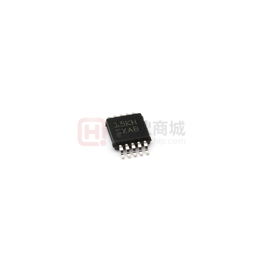
LM5060MM/NOPB
ACTIVE
VSSOP
DGS
10
1000
RoHS & Green
SN
Level-1-260C-UNLIM
-40 to 125
SXAB
LM5060MMX/NOPB
ACTIVE
VSSOP
DGS
10
3500
RoHS & Green
SN
Level-1-260C-UNLIM
-40 to 125
SXAB
LM5060Q1MM/NOPB
ACTIVE
VSSOP
DGS
10
1000
RoHS & Green
SN
Level-1-260C-UNLIM
-40 to 125
SZAB
LM5060Q1MMX/NOPB
ACTIVE
VSSOP
DGS
10
3500
RoHS & Green
SN
Level-1-260C-UNLIM
-40 to 125
SZAB
LM5060QDGSRQ1
ACTIVE
VSSOP
DGS
10
3500
RoHS & Green
SN
Level-1-260C-UNLIM
-40 to 125
1EQX
(1)
The marketing status values are defined as follows:
ACTIVE: Product device recommended for new designs.
LIFEBUY: TI has announced that the device will be discontinued, and a lifetime-buy period is in effect.
NRND: Not recommended for new designs. Device is in production to support existing customers, but TI does not recommend using this part in a new design.
PREVIEW: Device has been announced but is not in production. Samples may or may not be available.
OBSOLETE: TI has discontinued the production of the device.
(2)
RoHS: TI defines "RoHS" to mean semiconductor products that are compliant with the current EU RoHS requirements for all 10 RoHS substances, including the requirement that RoHS substance
do not exceed 0.1% by weight in homogeneous materials. Where designed to be soldered at high temperatures, "RoHS" products are suitable for use in specified lead-free processes. TI may
reference these types of products as "Pb-Free".
RoHS Exempt: TI defines "RoHS Exempt" to mean products that contain lead but are compliant with EU RoHS pursuant to a specific EU RoHS exemption.
Green: TI defines "Green" to mean the content of Chlorine (Cl) and Bromine (Br) based flame retardants meet JS709B low halogen requirements of