User's Guide
SNVA481B – October 2011 – Revised January 2020
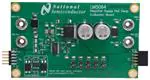
AN-2143 LM5064 Evaluation Kit
1
Introduction
The LM5064EVK evaluation module provides the power design engineer with a fully functional intelligent
monitoring and protection controller board designed for negative voltage systems. This application note
describes the various functions of the board, how to test and evaluate it, and how to use the GUI design
tool to change the components for a specific application. Use of the advanced telemetry and monitoring
capabilities of this device requires the installation of the Intelligent Power Manager GUI; however, the
LM5064 is capable of acting as a hot-swap and protection circuit without any software installation. Please
check the LM5064 Negative Voltage System Pwr Mgmt & Protection IC with PMBus (SNVS718) for the
latest software and data sheet information.
2
PCB Features
•
•
•
•
•
•
•
•
•
Operating input voltage range: –36 V to –60 V
Programmable current limit: set to 16.7 A (CL = VEE or HIGH-Z) or 8.7 A (CL = VDD)
Q1 power limit: 80W (typical)
UVLO thresholds: –36 V (falling) and –32 V (rising)
OVLO thresholds: –60 V (falling) and –56 V (rising)
Insertion delay: 125 ms
Fault time-out period: 8 ms
Restart time: 1.4 s
Digital isolation circuitry for all PMBusTM signals and PGOOD
SNVA481B – October 2011 – Revised January 2020
Submit Documentation Feedback
Copyright © 2011–2020, Texas Instruments Incorporated
AN-2143 LM5064 Evaluation Kit
1
�Simplified Schematic
3
www.ti.com
Simplified Schematic
GND1 (+)
GND2 (+)
R1
200 kŸ
R3
191 kŸ
VCC
UVLO/EN
VAUXH
OVLO
PGD
R2
16.9 kŸ
R4
8.25 kŸ
60V
5.0SMDJ60A
VAUX
R5
280 kŸ
R6
10.0 kŸ
SDAI
SDAO
SCL
SMBA
OUT
LM5064
GATE
CL
RETRY
ADR0
ADR1
ADR2
VAUX
SENSE
+
+
100 µF
CO1
100 µF
CO2
D1
B3100-13-F
SENSE_ K
VEE_K
VEE
VREF
TIMER
CREF
1 µF
VDD
PWR
CVDD
CT
0.15 µF 1 µF
DIODE
RPWR
30.1 kŸ
DTEMP
CMPT3904
RS
0.003
Q1
FDB047N10
VEE (-)
VEE_OUT (-)
Figure 1. Simplified Schematic
2
AN-2143 LM5064 Evaluation Kit
SNVA481B – October 2011 – Revised January 2020
Submit Documentation Feedback
Copyright © 2011–2020, Texas Instruments Incorporated
�Getting Started
www.ti.com
GND1_S
GND2_S
RIN
0Ÿ
GND1 (+)
R1
200 kŸ
UVLO/
EN
R3
191 kŸ
CIN
10 nF
U1
VCC
UVLO/EN
VAUXH
R2a
OVLO
PGD
SDAI
SDAO
SCL
SMBA
60V
5.0SMDJ60A
VAUX
R5
280 kŸ
VEE
PGD
OPEN
R4
8.25 kŸ
GND2 (+)
CAXH
OPEN
VEE
OVLO
R2
16.9 kŸ
RAXH
0Ÿ
VAUXH
OUT
GATE
LM5064
GATE
CL
RETRY
ADR0
ADR1
ADR2
VAUX
SENSE
100 µF
CO2
D1
B3100-13-F
CS
OPEN
VEE_K
VDD
TIMER
TIMER
DIODE
PWR
VDD
CREF
1 µF
RS1
0Ÿ
DTEMP
CMPT3904
CD
1000 pF
VEE_S
+
SENSE_ K
VEE
VREF
R6
10.0 kŸ
+
100 µF
CO1
RS-
RS+
RS
0.003
RPWR
30.1 kŸ
CT
CVDD
0.15 µF 1 µF
RS2
0Ÿ
VEE_OUT_S
DRAIN
Q1
FDB047N10
VEE (-)
ISOLATION
VEE_OUT (-)
SWITCHES
DVDD
VDD
ADR2
ADR1
VDD
ADR0
CL
RETRY
HIGH-Z
C2
1 µF
CONNECTORS
1
U1
Si4800
J2
DGND 1
SCL_ISO
SDA_ISO
DGND
SMBA_ISO
DVDD
R8
0Ÿ
AVDD
C1
1 µF
VEE
BVDD
SDA_ISO
ASDA BSDA
SCL_ISO
ASCL
RP1
10 kŸ
RP2
10 kŸ
VEE
SDAI/
SDAO
PGD
BSCL
SCL
DGND
1
AGND BGND
J1
SCL_ISO
SDA_ISO
SMBA_ISO
DGND
DGND
DVDD
R7
0Ÿ
VEE
DVDD
VDD
RP4
39.0 kŸ
PGD
U3
PS2501-1-A
PGOOD_ISO
RP6
10.0 kŸ
1
DGND
DVDD
SMBA_ISO
DGND
U4
RP5
PS2501-1-A
39.0 kŸ
1
PGOOD
VDD
RP3
4.99 kŸ
SMBA
DGND
Figure 2. Full Evaluation Board Schematic
The schematic for the LM5064 evaluation board is shown in Figure 2. Connections to the PMBus interface
are provided by J2. Banana connectors provide input and output connections. Pins ADR0, ADR1, and
ADR2 are connected to switches that set the PMBus address of the device to one of 27 unique
addresses. Pins RETRY and CL are also connected to switches, allowing for hardware programmability of
the retry and current limit parameters, respectively. Test points are provided to conveniently probe signals
of interest.
4
Getting Started
The LM5064 evaluation kit hardware is shown in Figure 3.
SNVA481B – October 2011 – Revised January 2020
Submit Documentation Feedback
Copyright © 2011–2020, Texas Instruments Incorporated
AN-2143 LM5064 Evaluation Kit
3
�Hardware Setup Steps
www.ti.com
The LM5064EVK is supplied with the PMBus address set to 0x16 as dictated by the switch configuration
of the ADR0, ADR1, and ADR2 jumper connections.
Figure 3. Connection Illustration
The first step to evaluate the telemetry features of LM5064 is to install the GUI software. The software is
included on a CD in the evaluation kit and is titled PMBManager-x.x.x-xxxxxxxx.exe, where the x
characters indicate the software version and build date. This file should be executed on a PC running
Windows XP or later to install the software. Once the GUI software is installed the hardware should be
configured as shown in Figure 3.
5
Hardware Setup Steps
1.
2.
3.
4.
Connect
Connect
Connect
Connect
the input supply to the GND1 (+) and VEE (-) banana plugs.
the load to the GND2 (+) and VEE_OUT (-) banana plugs.
the FTDI dongle to the 10 pin connector (J2) on the left side of the board.
the supplied mini USB cable from the FTDI dongle to an USB port on a PC.
When the FTDI dongle is connected for the first time the user will be prompted to install the device drivers.
For the most current driver installation procedure refer to the README.TXT file in the installation
directory.
For a hot swap circuit to function reliably, a low inductance connection to the input supply is
recommended. Its purpose is to minimize voltage transients which occur when the load current changes or
is shut off. If not careful, wiring inductance in the supply lines will generate a voltage transient at the input
which can exceed the absolute maximum rating of the LM5064, resulting in its destruction. To protect
against such voltage transients, TVS device Z1 is provided to clamp the voltage at the input to within safe
operating limits. Likewise, Schottky diode D1 is provided on the output to clamp the output from going
excessively positive during short circuit events.
6
Device Evaluation
After configuring the hardware connections, apply an input voltage of -48V to the device. The current
hardware configuration allows the LM5064 device to work from -36V to -60V input supply voltage;
however, this guide will assume an input voltage of -48V. Launch the GUI by going to the Windows Start
menu -> All Programs -> PMBManager-x.xxxxx -> PMBusManager. A pulldown menu should come up
with a list of devices populated. Select the "LM5064" option as shown in Figure 4.
Figure 4. Device Selector
4
AN-2143 LM5064 Evaluation Kit
SNVA481B – October 2011 – Revised January 2020
Submit Documentation Feedback
Copyright © 2011–2020, Texas Instruments Incorporated
�Device Evaluation
www.ti.com
The device should be detected on the PMBusand the initial load screen should appear as shown in
Figure 5.
Figure 5. Initial GUI Screen
If a device is not detected, an option is provided to rescan, ignore, or exit the GUI. If the hardware is
intended to be connected, check the USB connection to the PCB, FTDI connection to the evaluation
module, and verify that the power is present on the evaluation PCB by measuring the voltage between the
GND1_s (+) and VEE_s (-) testpoints. Ignoring the detection message allows use of the integrated design
tool without the hardware connected.
Device Telemetry
Telemetry Plotter
Device Information
Display Options
Design Tool
Device Configuration
Figure 6. LM5064 Block Level Representation
Double click on the detected device ID (NSC-LM5064-AA) to display a block level representation of the
device as shown in Figure 6. The block level view of the device provides a display of all the telemetry data
as well as most of the faults and warnings supported by the device. The faults and warnings supported
are generally associated with an invalid input or output condition.
SNVA481B – October 2011 – Revised January 2020
Submit Documentation Feedback
Copyright © 2011–2020, Texas Instruments Incorporated
AN-2143 LM5064 Evaluation Kit
5
�Device Evaluation
www.ti.com
The faults shown on the left side of the block representation are generally associated with the input. These
include input under-voltage (UV), input over-voltage (OV), FET Fail (FF), and input over-power (OP). The
SMBus alert status, SMBA, is also shown on the left side and will turn red during any warning or fault
event. To facilitate the evaluation of the device, SMBus alerts are automatically cleared by the GUI.
The faults shown on the right side of the block representation are associated with the output. These
include output over-voltage (OV), power good status (PGD), output over-current (OC), and overtemperature (OT). There is also an indicator if the output is in the latched off state (LO). The device will
latch the output off after the number of user programmable retries is exceeded. To clear the latched off
condition, the output can be toggled off and on by the red power button icon located in the top right of the
LM5064 block representation.
To show a repetitive update of the device telemetry and status click on the play icon at the top of the
screen. The play button starts an active telemetry log of the gathered data. Clicking the stop icon stops
the telemetry collection and allows for the log file to be viewed and saved. The pause button pauses both
the displaying and logging of telemetry information.
To disable displaying undesired telemetry click the display icon on the block representation. This will open
the window shown in Figure 7 that will allow the user to disable the undesired telemetry, fault, and warning
information from appearing on the block level device representation.
6
AN-2143 LM5064 Evaluation Kit
SNVA481B – October 2011 – Revised January 2020
Submit Documentation Feedback
Copyright © 2011–2020, Texas Instruments Incorporated
�GUI Event Log
www.ti.com
Figure 7. LM5064 Telemetry Display Options
Note that turning off the various warning options does not mask the faults from issuing an SMBus alert - it
just does not display them if they occur. The device is capable of masking various faults and this
functionality can be setup in the device configuration panel.
7
GUI Event Log
A GUI event log is provided to keep track of GUI configuration changes and device fault events. To
display the event log select View from the main menu bar and then View Event Log. The event log will
appear on the left side of the main GUI window. The event log can be detached and expanded if desired
by left clicking on the event log window and dragging window with the mouse to the desired location.
SNVA481B – October 2011 – Revised January 2020
Submit Documentation Feedback
Copyright © 2011–2020, Texas Instruments Incorporated
AN-2143 LM5064 Evaluation Kit
7
�Plotting Telemetry Data
8
www.ti.com
Plotting Telemetry Data
To enable telemetry data plots click on the sine wave icon located on the LM5064 block representation.
After enabling the telemetry, a prompt will appear requesting entry of the GUI sample rate, plot rate, and
plot depth. For most cases the default rates and depths will be acceptable. The plotting tool allows the
user to select the desired data to be plotted. Up to two different parameters may be plotted at the same
time as shown in Figure 8 .
Figure 8. LM5064 GUI with Telemetry Plotting Tool Enabled
Device telemetry data is plotted as a black line that continually updates as the device is queried. In
addition to the device data, the relevant warning and fault thresholds are also plotted. Warning thresholds
are shown as orange lines while fault thresholds are shown in red and blue.
By going to the plot menu option the user can disable the plotting grid as well as the warning and fault
lines.
9
Configuring the LM5064 Device
Warning Thresholds, Temperature Fault Threshold, Protection Ranges, Fault Masking, and Averaging can
be configured in the Device Configuration panel. This panel, shown in Figure 9, is enabled by clicking the
gear icon shown on the LM5064 block representation.
8
AN-2143 LM5064 Evaluation Kit
SNVA481B – October 2011 – Revised January 2020
Submit Documentation Feedback
Copyright © 2011–2020, Texas Instruments Incorporated
�Configuring the LM5064 Device
www.ti.com
Figure 9. Device Configuration Panel
SNVA481B – October 2011 – Revised January 2020
Submit Documentation Feedback
Copyright © 2011–2020, Texas Instruments Incorporated
AN-2143 LM5064 Evaluation Kit
9
�Customizing the Design
www.ti.com
The Warning and Fault Threshold tab allows configuration of the input under-voltage, input over-voltage,
output under-voltage, input over-current, input power, and over temperature warnings. This tab also allows
adjustment of the over-temperature fault threshold. Fault threshold for the input over- and under-voltage,
current limit, power limit, and power good are set by the hardware design. Decimal values for the
thresholds are shown in the text box located to the right of the slider bar. Above the decimal values setting
is the value of the setting in hexadecimal, which can be useful when developing software for this device.
The fault behavior tab allows the user to set the device fault configuration and fault masking. The fault
configuration section allows the user to set the number of retries, as well as the circuit breaker and current
limit thresholds. The number of retries can be set by the RETRY pin to be infinite or latched off. Through
software, the number of retries can be set to 0 (latch-off), 1, 2, 4, 8, 16 or infinite. The software settings
are independent of the hardware settings; however, if the power is cycled the device will default to values
dictated by the hardware. Current limit power-up values are also set by the hardware. The values for
current limit can be set to either 26 mV (CL = VDD) or 50 mV (CL = VEE). The circuit breaker threshold
can also be set in software to either 1.9 times or 3.9 times the current limit value. Fault masking is
possible for many of the device fault conditions. Fault conditions allow masking of both the MOSFET
response and the SMBus alert signal. Note that if a fault occurs repeatedly while the MOSFET is masked,
damage to the MOSFET may result. This feature is allowed primarily for debug purposes. Faults that do
not shut off the MOSFET, and only issue a SMBus alert, will also allow masking of the alert. Note the
power-up default setting for the power good signal is to mask the SMBus alert, in order to ensure that
SMBus alert is not asserted immediately after power-up.
For convenience, the Device Configuration Panel can be undocked by holding down the left mouse button
while the cursor is at the top of the panel and dragging it to where you would like it to be placed.
10
Customizing the Design
The GUI assumes the hardware configuration is set to default evaluation board configuration. If any of the
components are changed, the device hardware configuration needs to be updated in the design tool
section. To open the design tool click the wrench icon located on the LM5064 block representation which
will open the window displayed in Figure 10.
Figure 10. LM5064 Design Tool
10
AN-2143 LM5064 Evaluation Kit
SNVA481B – October 2011 – Revised January 2020
Submit Documentation Feedback
Copyright © 2011–2020, Texas Instruments Incorporated
�GUI Register Page
www.ti.com
Design inputs are keyed in on the left side following steps 1 though 5. General operating conditions should
be entered in step 1 of the design tool. These inputs help set bounds on the startup time and application
voltage ranges.
Step 2 allows the user to tailor the MOSFET protection features to be specific to the target application.
Current limit is pin-configurable and software configurable, and circuit breaker is software-configurable. If
CL switch is used to set the current limit, make sure the GUI selection matches the pin-configurable CL bit
setting on the board. By clicking on the MOSFET SOA Profile button the user can select SOA data from
several popular MOSFETs or enter the SOA data for the desired MOSFET. The resistor RPWR can then be
calculated to keep Q1 within its SOA profile.
Step 3 allows the user to select the under- and over-voltage lockout values (UVLO/OVLO). Note that with
the correct values for R1 - R4, the device will indicate a fault condition when the input and/or output
voltages are outside of their programmed range.
Step 4 allows the user to set the fault time-out period and the fault response. The fault time-out should be
set to be below the MOSFET SOA data for a given time. For example, if a design is done to adhere to the
10 ms pulsed MOSFET SOA data, the desired fault time-out must be less than 10 ms. The fault time-out
time entered will set the value for CT. It also sets the insertion delay and fault retry delay. The initial power
up retry behavior is also selected in this design step. Make sure to change the RETRY switch to match the
design tool schematic when changing the default retry setting.
In step 5 the user enters the desired PMBus address. Note changing the PMBus address of the device in
step 5 does not change the device address, but shows how the address pins of the device need to be
configured to achieve a desired address. Once the ADR pin switches are configured for a particular
address, power to the device needs to be cycled and the GUI restarted in order for the new address to
take affect.
When invalid or incorrect inputs are given to the design tool, text associated with the faulty input will turn
red. Positioning the mouse cursor over the red text will give additional information about any design
conflict.
Component and parametric results are shown to the right as well as the LM5064 protection SOA chart.
The protection SOA chart shows the minimum, typical, and maximum SOA protection areas for a given
design. For a robust design, the SOA of the MOSFET used should be above the MAX protection SOA line
for all operating areas.
Once a design is complete, the design should be saved by selecting the File menu, and then Save. Once
the hardware is modified to match the design the GUI should be restarted and the hardware configuration
file loaded right after the device is detected and placed. If the values in the design tool are different than
the values on the board, erroneous telemetry and fault data will be reported by the GUI. To return to the
block view of the device, press the home icon located at the far left in the menu bar.
The design tool is also useful to calculate the PMBus coefficients. With the correct value for current sense
resistor (RS) the tool will calculate the correct coefficients to scale the raw telemetry data. The coefficients
can be viewed by selecting View from the main menu bar, and then selecting the PMBus Coefficient
Editor. When the PMBus Coefficient Editor is opened, press the Get All button to show the currently used
coefficients.
If desired the results presented by the design tool can be calculated by hand using the equations provided
in the datasheet. However, note the design tool calculates parameters factoring in worst case tolerances,
while the equations in the data sheet are based on typical thresholds.
11
GUI Register Page
The GUI Register Page, as shown in Figure 11, provides the user with several features to help better
understand the functionality of the LM5064. These features include the ability to read telemetry, device
identification and status registers, as well as being able to monitor the SMBus Alert and PGOOD
interrupts, and to turn the output on and off with the OPERATION button.
SNVA481B – October 2011 – Revised January 2020
Submit Documentation Feedback
Copyright © 2011–2020, Texas Instruments Incorporated
AN-2143 LM5064 Evaluation Kit
11
�GUI Register Page
www.ti.com
Figure 11. LM5064 Register Page
Telemetry is updated by clicking the Update Telemetry button. This action will update the fields under the
Averaged heading and under the Immediate heading along with VAUX and PEAK PIN. Select which
parameters to update by clicking in the box next to each parameter. If all parameter boxes under a given
heading are checked, the "Update Telemetry" button will use the block read PMBus commands
(AVG_BLOCK_READ and BLOCK_READ) to update the fields, ensuring that the readings are time
aligned. If one or more of the boxes under the headings is not checked, the "Update Telemetry" button will
use the respective individual read PMBus commands to make the telemetry readings and the
measurements will not be time aligned. VAUX and PEAK PIN are always read with discrete PMBus
commands and, therefore, are never time aligned. The "CLEAR_PIN_PEAK" button is provided to clear
the PEAK PIN reading which is often much higher than one would expect under steady state conditions.
This is related to the large inrush current during power-on that gets sampled by the internal power
measurement circuitry and used to calculate PEAK PIN.
The output can be turned off and on using the "OPERATION" button, and the Identification Information
can be obtained by clicking the "Update ID Information" button. The rest of this page is used to monitor
and diagnose warning and fault conditions. The SMBA and PGOOD interrupts will indicate if a warning or
fault has occurred and if the output voltage is within specifications. They are always active and there is no
need to click an "Update Telemetry" button to change their state. Clicking the "Update Status" button
under the Register Operation Control heading will update the bits in all of the registers, as well as the
telemetry, under the Status section. Clicking the "CLEAR_FAULTS" button will reset all warning and fault
bits and issue an Update Status. If the warning and/or fault condition has been remedied, the bits will
reset. If the warning and/or fault condition still exists, the registers will be updated within a millisecond and
thus will appear to never have been cleared. The STATUS_WORD, STATUS_INPUT, STATUS_CML and
DIAGNOSTIC_WORD registers operate in a cumulative way. That is, these registers display any and all
warnings and errors that have occurred since the last CLEAR_FAULTS command was issued. The
telemetry and DIAGNOSTIC_WORD that are part of the BLACK_BOX_READ are also updated by clicking
the Update Status button. These telemetry parameters and bits are latched at the moment the SMBA
12
AN-2143 LM5064 Evaluation Kit
SNVA481B – October 2011 – Revised January 2020
Submit Documentation Feedback
Copyright © 2011–2020, Texas Instruments Incorporated
�Theory of Operation
www.ti.com
signal was asserted. They are not reset or cleared by the CLEAR_FAULTS command but rather, they are
re-armed, or readied, to be over-written with new values at the onset of the next SMBA signal assertion.
Note that these telemetry fields and this register are not cumulative. That is, they can only be updated
once after the CLEAR_FAULTS command is issued, and it will be at the first occurrence of the SMBA
assertion following the CLEAR_FAULTS. This allows the user to determine device conditions at the first
occurrence of the SMBA assertion.
12
Theory of Operation
The LM5064 provides intelligent control of the power to a load from a live power source. The three primary
functions of the device are to limit inrush current during turn-on, monitor the load current for faults during
normal operation, and to provide system telemetry for the following parameters: Input Voltage (VCC to
VEE), Input Current (IIN), Input Power (PIN), Output Voltage (VOUT), Auxilliary Voltage (VAUX), and
Temperature. Additional functions include under- and over-voltage lock-outs (UVLO/OVLO) to ensure
voltage is supplied to the load only when the system input voltage is within a specified range, power
limiting of the series pass MOSFET (Q1) during turn-on, and a Power Good logic output (PGD) to indicate
the output voltage status.
Upon applying the input voltage to the LM5064, Q1 is initially held off for the insertion delay (125 ms) to
allow ringing and transients on the input to subside. At the end of the insertion delay, if the input voltage
(VCC-VEE) is above the UVLO threshold, Q1 is turned on in a controlled manner to limit the inrush
current.
The LM5064 utilizes two methods to limit inrush currents at startup. For the input voltage range and sense
resistor on this board, the inrush current will be limited by the MOSFET power limit method. The power
limit method controls the input current such that a constant power is dissipated by Q1 during startup. At
the onset of the startup period, Vsys (VEE)= -48V and VOUT = 0V. Q1’s power dissipation is limited to a
peak value set by RPWR (80W) by monitoring its drain current (the voltage across RS) and its drain-tosource voltage. Their product is maintained constant by controlling the drain current as the drain-to-source
voltage decreases (as the output voltage increases). This is shown in the constant power portion of where
the drain current is increasing to ILIM.
0
VDS
VSYS
IDS
0
PMOSFET
PLIM
VGATE
Gate - to - Source Voltage
VGSL
VTH
t ON
VSYS
0
t3
t1 t2
a) Power Limit
Figure 12. Power Up Using Power Limit
SNVA481B – October 2011 – Revised January 2020
Submit Documentation Feedback
Copyright © 2011–2020, Texas Instruments Incorporated
AN-2143 LM5064 Evaluation Kit
13
�Fault Detection & Restart
www.ti.com
If the power across Q1 does not exceed the programmed power limit, the LM5064 will also limit the drain
current to the current limit value determined by the sense resistance and the selected current limit voltage
threshold, 26 mV or 50 mV. The current limit will be maintained constant as the output voltage continues
to increase. During the current limit period, the voltage at the TIMER pin will be rising. If the TIMER
voltage reaches 3.9V before the current limit time has expired, the device will shut down and retry
according to the programmed retry configuration. If the TIMER does not expire, the output voltage will rise
and the drain current needed to charge the output capacitance will reduce. The output voltage will
continue to rise towards the the input voltage (VDS decreases to near zero), and the drain current then
reduces to a value determined by the load. Q1’s gate-to-source voltage then increases to its final value.
The circuit is now in normal operation mode.
Monitoring of the load current for faults during normal operation is accomplished using the current limit
circuit described above. If the load current increases to 8.7 Amps (26 mV across RS), Q1’s gate is
controlled to prevent the current from increasing further. When current limiting takes effect, the fault timer
limits the duration of the fault. At the end of the fault time-out period Q1 is shut off, denying current to the
load. The LM5064 then initiates a restart every 1.4 seconds. The restart consists of turning on Q1 and
monitoring the load current to determine if the fault is still present. After the fault is removed, the circuit
powers up to normal operation at the next restart. If the retry setting is changed to a limited number of
retrys, the LM5064 will stop retrying after the programmed number of retrys occur, and keep Q1 shut off
until UVLO/EN is toggled or the output is turned off and then on via PMBus.
In a sudden overload condition (e.g. when the output is shorted to VEE), it is possible that the current
could increase faster than the response time of the current limit circuit. In this case, the circuit breaker
sensor shuts off Q1’s gate rapidly when the voltage across RS reaches 49 mV. When the current reduces
to the current limit threshold, the current limit circuitry then takes over.
The PGD logic level output is low during turn-on and switches high when the VDS of the MOSFET is
below 1.25V. PGD switches low when the VDS of the MOSFET is above 2.5V. The high level voltage at
PGD can be any appropriate voltage up to +80V above VEE and can be higher or lower than the voltages
at VCC and OUT.
The UVLO thresholds are set by resistors R1 and R2, the OVLO thresholds are set by R3 and R4.
Optional resistor R2a can be added to set the UVLO and OVLO thresholds with only three resistors as
outlined in the LM5064 datasheet. Internal current sources at UVLO/EN and OVLO are used to set the
hysteresis levels.
13
Fault Detection & Restart
If the load current increases to the fault level (the typical current limit threshold of 8.7A), an internal current
source charges the timing capacitor at the TIMER pin. When the voltage at the TIMER pin reaches 3.9V,
the fault time-out period is complete and the LM5064 shuts off Q1. The restart sequence then begins,
consisting of seven cycles at the TIMER pin between 3.9V and 1.2V, as shown in Figure 13. When the
voltage at the TIMER pin reaches 0.3V during the eighth high-to-low ramp, Q1 is turned on. If the fault is
still present, the fault time-out period and the restart sequence repeat.
Fault
Detection
I LIMIT
Load
Current
GATE
Pin
TIMER
Pin
52 PA
Gate Charge
4.1 mA
pulldown
2.4 PA
3.9V
74 PA
1.2V
1
Fault Timeout
Period
2
3
7
8
0.3V
t RESTART
Figure 13. Fault Time-out and Restart Sequence
14
AN-2143 LM5064 Evaluation Kit
SNVA481B – October 2011 – Revised January 2020
Submit Documentation Feedback
Copyright © 2011–2020, Texas Instruments Incorporated
�UVLO and OVLO Input Voltage Threshold
www.ti.com
The waveform at the TIMER pin can be monitored at the TIMER test point. On this evaluation board, the
initial fault time-out period is 8 ms and the restart time is 1.4 seconds.
14
UVLO and OVLO Input Voltage Threshold
Programming the UVLO threshold sets the minimum system voltage to enable Q1. If VCC-VEE is below
the UVLO thresholds, Q1 is switched off, denying power to the load. Programmable hysteresis is
adjustable by changing the value of R1.
The UVLO threshold is set with two resistors (R1, R2) as shown in Figure 14 and an internal 20 µA
current source allows a hysteresis voltage to be set.
The OVLO threshold sets the maximum voltage that can be present on the input before the device turns
off the series pass device. The OVLO threshold is set with the two resistors (R3, R4). The hysterisis
voltage is set by the internal 21 uA current source and the value of R3.
GND
VCC
R3
R1
R2a
20 PA
LM5064
UVLO/
EN
2.48V
R4/3a
TIMER AND GATE
LOGIC CONTROL
R2
2.47V
OVLO
VEE
21 PA
VSYS
Figure 14. Programming the UVLO and OVLO Thresholds
15
Shutdown
With the circuit in normal operation, the LM5064 can be shutdown by pulling the UVLO/EN pin to VEE or
by clicking the ON/OFF button on the LM5064 block representation in the GUI.
16
Board Layout and Probing Cautions
Refer to the product datasheet for detailed layout guidelines. For most applications the layout of this
evaluation module as detailed in the PC Board Layout section of this document should be sufficient to
provide a working solution with accurate telemetry. The following should be kept in mind when the board is
powered:
1. Use CAUTION when probing the circuit to prevent injury as well as possible damage to the circuit.
2. At maximum load current ( typically 16.7A), the wire size and length used to connect the power source
and the load become very important. The wires connecting this evaluation board to the power source
should be a heavy gauge and twisted together to minimize input inductance. The same applies for the
wires connecting this board to the load. This recommendation is made in order to minimize high
voltage transients from occurring when the load current is shut off.
3. A 60V TVS diode located close to the LM5064EVK GND1 and VEE pins provides the critical function
of clamping inevitable input voltage overshoot when Q1 turns off at high currents. If operation above
60V is required, the TVS will need to be replaced with a TVS rated at a higher standoff voltage. Always
verify the TVS by performing a worst-case current limit at the maximum input voltage and monitoring
the resulting input voltage surge. The TVS should be able to clamp the input below 100V in all cases.
4. The VEE points for the UVLO/EN and OVLO resistor networks are tied directly to a via where the
SNVA481B – October 2011 – Revised January 2020
Submit Documentation Feedback
Copyright © 2011–2020, Texas Instruments Incorporated
AN-2143 LM5064 Evaluation Kit
15
�Performance Characteristics
www.ti.com
LM5064 is conneced to the VEE plane.
5. All testpoint signals are referenced to the VEE voltage.
17
Performance Characteristics
VTIMER (2V/Div)
VTIMER (2V/Div)
VOUT (20V/Div)
VOUT (20V/Div)
VSYS (20V/Div)
VSYS (5V/Div)
IIN (5A/Div)
IIN (5A/Div)
Figure 15. Insertion Time Delay (40 ms/div)
Figure 16. Turn-On Sequence into a 40Ω Load (40 ms/div)
VTIMER (2V/Div)
VTIMER (2V/Div)
VGATE (5V/Div)
VOUT (20V/Div)
VGATE (5V/Div)
CL = 8.7A
CB = 1.8 x CL
VOUT (20V/Div)
IIN (5A/Div)
IIN (5A/Div)
Figure 17. Circuit Breaker Event (CL = VDD) 4 ms/div
Figure 18. Current Limit Event (CL = VDD) 4 ms/div
VGATE (20V/Div)
VOUT (20V/Div)
VSYS (25V/Div)
VSYS (20V/Div) (-48V)
VOUT (25V/Div)
VTIMER (2V/Div)
VGATE (20V/Div)
Figure 19. Startup (UVLO/EN, OVLO) (400 ms/div)
16
AN-2143 LM5064 Evaluation Kit
Figure 20. Short Circuit VOUT 1 s/div
SNVA481B – October 2011 – Revised January 2020
Submit Documentation Feedback
Copyright © 2011–2020, Texas Instruments Incorporated
�Performance Characteristics
www.ti.com
1.6
1.0
1.2
0.8
PIN ERROR (%)
IIN ERROR (%)
0.4
0.0
-0.4
-0.8
CL=VEE
0.4
0.2
0.0
-0.2
-0.4
-0.6
-1.2
-0.8
-1.6
-50
0.6
CL=VEE
0.8
-1.0
-25
0
25 50 75 100 125
TEMPERATURE (°C)
Figure 21. IIN Error vs Temperature
-50
-25
0
25 50 75 100 125
TEMPERATURE (°C)
Figure 22. PIN Error vs Temperature
SNVA481B – October 2011 – Revised January 2020
Submit Documentation Feedback
Copyright © 2011–2020, Texas Instruments Incorporated
AN-2143 LM5064 Evaluation Kit
17
�Bill of Materials
18
www.ti.com
Bill of Materials
Designator
Value
Description
Manufacturer
Part Number
Qty.
NEGATIVE HOT SWAP CONTROLLER
Texas
Instruments
LM5064
1
U2
BiDirectional I2C Isolator
Silicon Labs
Si8400
1
U3, U4
HIGH ISOLATION VOLTAGE SINGLE
TRANSISTOR TYPE
NEC
PS2501L-1-A
2
U1
C1, C2,
CREF, CVDD
1 µF
CAP, CERM, 1uF, 10V, +/-10%, X7R, 0603
MuRata
GRM188R71A105KA61D
4
CAXH
N/A
OPEN
N/A
N/A
N/A
CD, CS
1000
pF
CAP, CERM, 1000pF, 50V, +/-10%, X7R,
0603
MuRata
GRM188R71H102KA01D
2
CIN
10 nF
CAP, CERM, 0.01uF, 100V, +/-10%, X7R,
0805
MuRata
GRM21BR72A103KA01L
1
CO1, CO2
100 µF
CAP, AL, 100uF, 100V, +/-20%, SMD
Nippon ChemiCon
EMVE101ARA101MKE0S
1
CT
.15 µF
CAP, CERM, 0.15uF, 25V, +/-10%, X7R,
0603
MuRata
GRM188R71E154KA01D
1
D1
Diode, Schottky, 100V, 3A, SMC
Diodes Inc.
B3100-13-F
1
DTEMP
Transistor, NPN, 40V, 0.2A, SOT-23
NXP
Semiconductor
PMS3904
1
Q1
MOSFET, N-CH, 100V, 120A, DDPAK
Fairchild
FDB047N10
1
R1
200 kΩ
RES, 200 kΩ, 1%, 0.1W, 0603
Vishay-Dale
CRCW0603200KFKEA
1
R3
191 kΩ
RES, 191 kΩ, 1%, 0.1W, 0603
Vishay-Dale
CRCW0603191KFKEA
1
R2
16.9
kΩ
RES, 16.9 kΩ, 1%, 0.1W, 0603
Vishay-Dale
CRCW060316K9FKEA
1
R2a
N/A
OPEN
N/A
N/A
N/A
R4/3a
8.25
kΩ
RES, 8.25 kΩ, 1%, 0.1W, 0603
Vishay-Dale
CRCW06038K25FKEA
1
R5
280 kΩ
RES, 280 kΩ, 1%, 0.1W, 0603
Vishay-Dale
CRCW0603280KFKEA
1
R6, RP1, RP2
10 kΩ
RES, 10.0 kΩ, 1%, 0.1W, 0603
Vishay-Dale
CRCW060310K0FKEA
3
R7, R8,
RAXH, RS1,
RS2
0Ω
RES, 0Ω, 5%, 0.1W, 0603
Vishay-Dale
CRCW06030000Z0EA
1
RIN
0Ω
RES, 0Ω, 5%, 0.25W, 1206
Vishay-Dale
CRCW12060000Z0EA
1
RP3
4.99
kΩ
RES, 4.99 kΩ, 1%, 0.1W, 0603
Vishay-Dale
CRCW06034K99FKEA
1
RP4, RP5
39 kΩ
RES, 39 kΩ, 5%, 0.1W, 0603
Vishay-Dale
CRCW060339K0JNEA
1
RP6
10 kΩ
RES, 10 kΩ, 5%, 0.1W, 0603
Vishay-Dale
CRCW060310K0JNEA
1
RPWR
30.1
kΩ
RES, 30.1 kΩ, 1%, 0.1W, 0603
Vishay-Dale
CRCW060330K1FKEA
1
RS
3 mΩ
RES, 0.003Ω, 1%, 1W, 2512 SMD
Vishay-Dale
WSL25123L000FEA
1
RPWR
30.1
kΩ
RES, 30.1 kΩ, 1%, 0.1W, 0603
Vishay-Dale
CRCW060330K1FKEA
1
Transient Voltage Supression Diode,
5000W, 60V
Littlefuse
5.0SMDJ60A
1
Z1
18
AN-2143 LM5064 Evaluation Kit
SNVA481B – October 2011 – Revised January 2020
Submit Documentation Feedback
Copyright © 2011–2020, Texas Instruments Incorporated
�Bill of Materials
www.ti.com
Designator
Value
Description
Manufacturer
Part Number
Qty.
AD0, AD1,
AD2, CL,
DRAIN,
GATE,
GND1_S,
GND2_S,
OVLO,
PGOOD,
RS+, RS-,
RTRY,
TIMER,
UVLO, VAUX,
VAUXH, VDD,
VEE_OUT_S,
VEE_S
Test Point, TH, Miniature
Keystone
Electronics
5015
20
ADR0, ADR1,
ADR2,
CLIMIT,
RETRY
SWITCH SLIDE SPDT SMD J-LEAD 50 V,
100 mA
Copal
CJS-1201TA
5
GND1, GND2,
VEE,
VEE_OUT
Standard Banana Jack, Uninsulated
Keystone
Electronics
575-8
1
H1, H2, H5,
H6
Standoff, Hex, 0.5"L #4-40 Nylon
Keystone
Electronics
1902C
4
H3, H4, H7,
H8
'Machine Screw, Round, #4-40 x 1/4,
Nylon, Philips panhead
B Fastener
Supply
NY PMS 440 0025 PH
1
J1
Female Header, 5-Pin, Dual row, Right
Angle
Sullins
PPPC052LJBN-RC
1
J2
Male Header, 5-Pin, Dual row, Right Angle
Samtec Inc
TSW-105-08-L-D-RA
1
SNVA481B – October 2011 – Revised January 2020
Submit Documentation Feedback
Copyright © 2011–2020, Texas Instruments Incorporated
AN-2143 LM5064 Evaluation Kit
19
�PC Board Layout
19
www.ti.com
PC Board Layout
Figure 23. Board Top Layer
Figure 24. Board Mid Layer 1
Figure 25. Board Mid Layer 2
20
AN-2143 LM5064 Evaluation Kit
SNVA481B – October 2011 – Revised January 2020
Submit Documentation Feedback
Copyright © 2011–2020, Texas Instruments Incorporated
�PC Board Layout
www.ti.com
Figure 26. Board Bottom Layer (viewed from top)
SNVA481B – October 2011 – Revised January 2020
Submit Documentation Feedback
Copyright © 2011–2020, Texas Instruments Incorporated
AN-2143 LM5064 Evaluation Kit
21
�Revision History
www.ti.com
Revision History
Changes from A Revision (May 2013) to B Revision ...................................................................................................... Page
•
22
Updated Figure 2 .......................................................................................................................... 3
Revision History
SNVA481B – October 2011 – Revised January 2020
Submit Documentation Feedback
Copyright © 2011–2020, Texas Instruments Incorporated
�STANDARD TERMS FOR EVALUATION MODULES
1.
Delivery: TI delivers TI evaluation boards, kits, or modules, including any accompanying demonstration software, components, and/or
documentation which may be provided together or separately (collectively, an “EVM” or “EVMs”) to the User (“User”) in accordance
with the terms set forth herein. User's acceptance of the EVM is expressly subject to the following terms.
1.1 EVMs are intended solely for product or software developers for use in a research and development setting to facilitate feasibility
evaluation, experimentation, or scientific analysis of TI semiconductors products. EVMs have no direct function and are not
finished products. EVMs shall not be directly or indirectly assembled as a part or subassembly in any finished product. For
clarification, any software or software tools provided with the EVM (“Software”) shall not be subject to the terms and conditions
set forth herein but rather shall be subject to the applicable terms that accompany such Software
1.2 EVMs are not intended for consumer or household use. EVMs may not be sold, sublicensed, leased, rented, loaned, assigned,
or otherwise distributed for commercial purposes by Users, in whole or in part, or used in any finished product or production
system.
2
Limited Warranty and Related Remedies/Disclaimers:
2.1 These terms do not apply to Software. The warranty, if any, for Software is covered in the applicable Software License
Agreement.
2.2 TI warrants that the TI EVM will conform to TI's published specifications for ninety (90) days after the date TI delivers such EVM
to User. Notwithstanding the foregoing, TI shall not be liable for a nonconforming EVM if (a) the nonconformity was caused by
neglect, misuse or mistreatment by an entity other than TI, including improper installation or testing, or for any EVMs that have
been altered or modified in any way by an entity other than TI, (b) the nonconformity resulted from User's design, specifications
or instructions for such EVMs or improper system design, or (c) User has not paid on time. Testing and other quality control
techniques are used to the extent TI deems necessary. TI does not test all parameters of each EVM.
User's claims against TI under this Section 2 are void if User fails to notify TI of any apparent defects in the EVMs within ten (10)
business days after delivery, or of any hidden defects with ten (10) business days after the defect has been detected.
2.3 TI's sole liability shall be at its option to repair or replace EVMs that fail to conform to the warranty set forth above, or credit
User's account for such EVM. TI's liability under this warranty shall be limited to EVMs that are returned during the warranty
period to the address designated by TI and that are determined by TI not to conform to such warranty. If TI elects to repair or
replace such EVM, TI shall have a reasonable time to repair such EVM or provide replacements. Repaired EVMs shall be
warranted for the remainder of the original warranty period. Replaced EVMs shall be warranted for a new full ninety (90) day
warranty period.
WARNING
Evaluation Kits are intended solely for use by technically qualified,
professional electronics experts who are familiar with the dangers
and application risks associated with handling electrical mechanical
components, systems, and subsystems.
User shall operate the Evaluation Kit within TI’s recommended
guidelines and any applicable legal or environmental requirements
as well as reasonable and customary safeguards. Failure to set up
and/or operate the Evaluation Kit within TI’s recommended
guidelines may result in personal injury or death or property
damage. Proper set up entails following TI’s instructions for
electrical ratings of interface circuits such as input, output and
electrical loads.
NOTE:
EXPOSURE TO ELECTROSTATIC DISCHARGE (ESD) MAY CAUSE DEGREDATION OR FAILURE OF THE EVALUATION
KIT; TI RECOMMENDS STORAGE OF THE EVALUATION KIT IN A PROTECTIVE ESD BAG.
�www.ti.com
3
Regulatory Notices:
3.1 United States
3.1.1
Notice applicable to EVMs not FCC-Approved:
FCC NOTICE: This kit is designed to allow product developers to evaluate electronic components, circuitry, or software
associated with the kit to determine whether to incorporate such items in a finished product and software developers to write
software applications for use with the end product. This kit is not a finished product and when assembled may not be resold or
otherwise marketed unless all required FCC equipment authorizations are first obtained. Operation is subject to the condition
that this product not cause harmful interference to licensed radio stations and that this product accept harmful interference.
Unless the assembled kit is designed to operate under part 15, part 18 or part 95 of this chapter, the operator of the kit must
operate under the authority of an FCC license holder or must secure an experimental authorization under part 5 of this chapter.
3.1.2
For EVMs annotated as FCC – FEDERAL COMMUNICATIONS COMMISSION Part 15 Compliant:
CAUTION
This device complies with part 15 of the FCC Rules. Operation is subject to the following two conditions: (1) This device may not
cause harmful interference, and (2) this device must accept any interference received, including interference that may cause
undesired operation.
Changes or modifications not expressly approved by the party responsible for compliance could void the user's authority to
operate the equipment.
FCC Interference Statement for Class A EVM devices
NOTE: This equipment has been tested and found to comply with the limits for a Class A digital device, pursuant to part 15 of
the FCC Rules. These limits are designed to provide reasonable protection against harmful interference when the equipment is
operated in a commercial environment. This equipment generates, uses, and can radiate radio frequency energy and, if not
installed and used in accordance with the instruction manual, may cause harmful interference to radio communications.
Operation of this equipment in a residential area is likely to cause harmful interference in which case the user will be required to
correct the interference at his own expense.
FCC Interference Statement for Class B EVM devices
NOTE: This equipment has been tested and found to comply with the limits for a Class B digital device, pursuant to part 15 of
the FCC Rules. These limits are designed to provide reasonable protection against harmful interference in a residential
installation. This equipment generates, uses and can radiate radio frequency energy and, if not installed and used in accordance
with the instructions, may cause harmful interference to radio communications. However, there is no guarantee that interference
will not occur in a particular installation. If this equipment does cause harmful interference to radio or television reception, which
can be determined by turning the equipment off and on, the user is encouraged to try to correct the interference by one or more
of the following measures:
•
•
•
•
Reorient or relocate the receiving antenna.
Increase the separation between the equipment and receiver.
Connect the equipment into an outlet on a circuit different from that to which the receiver is connected.
Consult the dealer or an experienced radio/TV technician for help.
3.2 Canada
3.2.1
For EVMs issued with an Industry Canada Certificate of Conformance to RSS-210 or RSS-247
Concerning EVMs Including Radio Transmitters:
This device complies with Industry Canada license-exempt RSSs. Operation is subject to the following two conditions:
(1) this device may not cause interference, and (2) this device must accept any interference, including interference that may
cause undesired operation of the device.
Concernant les EVMs avec appareils radio:
Le présent appareil est conforme aux CNR d'Industrie Canada applicables aux appareils radio exempts de licence. L'exploitation
est autorisée aux deux conditions suivantes: (1) l'appareil ne doit pas produire de brouillage, et (2) l'utilisateur de l'appareil doit
accepter tout brouillage radioélectrique subi, même si le brouillage est susceptible d'en compromettre le fonctionnement.
Concerning EVMs Including Detachable Antennas:
Under Industry Canada regulations, this radio transmitter may only operate using an antenna of a type and maximum (or lesser)
gain approved for the transmitter by Industry Canada. To reduce potential radio interference to other users, the antenna type
and its gain should be so chosen that the equivalent isotropically radiated power (e.i.r.p.) is not more than that necessary for
successful communication. This radio transmitter has been approved by Industry Canada to operate with the antenna types
listed in the user guide with the maximum permissible gain and required antenna impedance for each antenna type indicated.
Antenna types not included in this list, having a gain greater than the maximum gain indicated for that type, are strictly prohibited
for use with this device.
2
�www.ti.com
Concernant les EVMs avec antennes détachables
Conformément à la réglementation d'Industrie Canada, le présent émetteur radio peut fonctionner avec une antenne d'un type et
d'un gain maximal (ou inférieur) approuvé pour l'émetteur par Industrie Canada. Dans le but de réduire les risques de brouillage
radioélectrique à l'intention des autres utilisateurs, il faut choisir le type d'antenne et son gain de sorte que la puissance isotrope
rayonnée équivalente (p.i.r.e.) ne dépasse pas l'intensité nécessaire à l'établissement d'une communication satisfaisante. Le
présent émetteur radio a été approuvé par Industrie Canada pour fonctionner avec les types d'antenne énumérés dans le
manuel d’usage et ayant un gain admissible maximal et l'impédance requise pour chaque type d'antenne. Les types d'antenne
non inclus dans cette liste, ou dont le gain est supérieur au gain maximal indiqué, sont strictement interdits pour l'exploitation de
l'émetteur
3.3 Japan
3.3.1
Notice for EVMs delivered in Japan: Please see http://www.tij.co.jp/lsds/ti_ja/general/eStore/notice_01.page 日本国内に
輸入される評価用キット、ボードについては、次のところをご覧ください。
http://www.tij.co.jp/lsds/ti_ja/general/eStore/notice_01.page
3.3.2
Notice for Users of EVMs Considered “Radio Frequency Products” in Japan: EVMs entering Japan may not be certified
by TI as conforming to Technical Regulations of Radio Law of Japan.
If User uses EVMs in Japan, not certified to Technical Regulations of Radio Law of Japan, User is required to follow the
instructions set forth by Radio Law of Japan, which includes, but is not limited to, the instructions below with respect to EVMs
(which for the avoidance of doubt are stated strictly for convenience and should be verified by User):
1.
2.
3.
Use EVMs in a shielded room or any other test facility as defined in the notification #173 issued by Ministry of Internal
Affairs and Communications on March 28, 2006, based on Sub-section 1.1 of Article 6 of the Ministry’s Rule for
Enforcement of Radio Law of Japan,
Use EVMs only after User obtains the license of Test Radio Station as provided in Radio Law of Japan with respect to
EVMs, or
Use of EVMs only after User obtains the Technical Regulations Conformity Certification as provided in Radio Law of Japan
with respect to EVMs. Also, do not transfer EVMs, unless User gives the same notice above to the transferee. Please note
that if User does not follow the instructions above, User will be subject to penalties of Radio Law of Japan.
【無線電波を送信する製品の開発キットをお使いになる際の注意事項】 開発キットの中には技術基準適合証明を受けて
いないものがあります。 技術適合証明を受けていないもののご使用に際しては、電波法遵守のため、以下のいずれかの
措置を取っていただく必要がありますのでご注意ください。
1.
2.
3.
電波法施行規則第6条第1項第1号に基づく平成18年3月28日総務省告示第173号で定められた電波暗室等の試験設備でご使用
いただく。
実験局の免許を取得後ご使用いただく。
技術基準適合証明を取得後ご使用いただく。
なお、本製品は、上記の「ご使用にあたっての注意」を譲渡先、移転先に通知しない限り、譲渡、移転できないものとします。
上記を遵守頂けない場合は、電波法の罰則が適用される可能性があることをご留意ください。 日本テキサス・イ
ンスツルメンツ株式会社
東京都新宿区西新宿6丁目24番1号
西新宿三井ビル
3.3.3
Notice for EVMs for Power Line Communication: Please see http://www.tij.co.jp/lsds/ti_ja/general/eStore/notice_02.page
電力線搬送波通信についての開発キットをお使いになる際の注意事項については、次のところをご覧ください。http:/
/www.tij.co.jp/lsds/ti_ja/general/eStore/notice_02.page
3.4 European Union
3.4.1
For EVMs subject to EU Directive 2014/30/EU (Electromagnetic Compatibility Directive):
This is a class A product intended for use in environments other than domestic environments that are connected to a
low-voltage power-supply network that supplies buildings used for domestic purposes. In a domestic environment this
product may cause radio interference in which case the user may be required to take adequate measures.
3
�www.ti.com
4
EVM Use Restrictions and Warnings:
4.1 EVMS ARE NOT FOR USE IN FUNCTIONAL SAFETY AND/OR SAFETY CRITICAL EVALUATIONS, INCLUDING BUT NOT
LIMITED TO EVALUATIONS OF LIFE SUPPORT APPLICATIONS.
4.2 User must read and apply the user guide and other available documentation provided by TI regarding the EVM prior to handling
or using the EVM, including without limitation any warning or restriction notices. The notices contain important safety information
related to, for example, temperatures and voltages.
4.3 Safety-Related Warnings and Restrictions:
4.3.1
User shall operate the EVM within TI’s recommended specifications and environmental considerations stated in the user
guide, other available documentation provided by TI, and any other applicable requirements and employ reasonable and
customary safeguards. Exceeding the specified performance ratings and specifications (including but not limited to input
and output voltage, current, power, and environmental ranges) for the EVM may cause personal injury or death, or
property damage. If there are questions concerning performance ratings and specifications, User should contact a TI
field representative prior to connecting interface electronics including input power and intended loads. Any loads applied
outside of the specified output range may also result in unintended and/or inaccurate operation and/or possible
permanent damage to the EVM and/or interface electronics. Please consult the EVM user guide prior to connecting any
load to the EVM output. If there is uncertainty as to the load specification, please contact a TI field representative.
During normal operation, even with the inputs and outputs kept within the specified allowable ranges, some circuit
components may have elevated case temperatures. These components include but are not limited to linear regulators,
switching transistors, pass transistors, current sense resistors, and heat sinks, which can be identified using the
information in the associated documentation. When working with the EVM, please be aware that the EVM may become
very warm.
4.3.2
EVMs are intended solely for use by technically qualified, professional electronics experts who are familiar with the
dangers and application risks associated with handling electrical mechanical components, systems, and subsystems.
User assumes all responsibility and liability for proper and safe handling and use of the EVM by User or its employees,
affiliates, contractors or designees. User assumes all responsibility and liability to ensure that any interfaces (electronic
and/or mechanical) between the EVM and any human body are designed with suitable isolation and means to safely
limit accessible leakage currents to minimize the risk of electrical shock hazard. User assumes all responsibility and
liability for any improper or unsafe handling or use of the EVM by User or its employees, affiliates, contractors or
designees.
4.4 User assumes all responsibility and liability to determine whether the EVM is subject to any applicable international, federal,
state, or local laws and regulations related to User’s handling and use of the EVM and, if applicable, User assumes all
responsibility and liability for compliance in all respects with such laws and regulations. User assumes all responsibility and
liability for proper disposal and recycling of the EVM consistent with all applicable international, federal, state, and local
requirements.
5.
Accuracy of Information: To the extent TI provides information on the availability and function of EVMs, TI attempts to be as accurate
as possible. However, TI does not warrant the accuracy of EVM descriptions, EVM availability or other information on its websites as
accurate, complete, reliable, current, or error-free.
6.
Disclaimers:
6.1 EXCEPT AS SET FORTH ABOVE, EVMS AND ANY MATERIALS PROVIDED WITH THE EVM (INCLUDING, BUT NOT
LIMITED TO, REFERENCE DESIGNS AND THE DESIGN OF THE EVM ITSELF) ARE PROVIDED "AS IS" AND "WITH ALL
FAULTS." TI DISCLAIMS ALL OTHER WARRANTIES, EXPRESS OR IMPLIED, REGARDING SUCH ITEMS, INCLUDING BUT
NOT LIMITED TO ANY EPIDEMIC FAILURE WARRANTY OR IMPLIED WARRANTIES OF MERCHANTABILITY OR FITNESS
FOR A PARTICULAR PURPOSE OR NON-INFRINGEMENT OF ANY THIRD PARTY PATENTS, COPYRIGHTS, TRADE
SECRETS OR OTHER INTELLECTUAL PROPERTY RIGHTS.
6.2 EXCEPT FOR THE LIMITED RIGHT TO USE THE EVM SET FORTH HEREIN, NOTHING IN THESE TERMS SHALL BE
CONSTRUED AS GRANTING OR CONFERRING ANY RIGHTS BY LICENSE, PATENT, OR ANY OTHER INDUSTRIAL OR
INTELLECTUAL PROPERTY RIGHT OF TI, ITS SUPPLIERS/LICENSORS OR ANY OTHER THIRD PARTY, TO USE THE
EVM IN ANY FINISHED END-USER OR READY-TO-USE FINAL PRODUCT, OR FOR ANY INVENTION, DISCOVERY OR
IMPROVEMENT, REGARDLESS OF WHEN MADE, CONCEIVED OR ACQUIRED.
7.
4
USER'S INDEMNITY OBLIGATIONS AND REPRESENTATIONS. USER WILL DEFEND, INDEMNIFY AND HOLD TI, ITS
LICENSORS AND THEIR REPRESENTATIVES HARMLESS FROM AND AGAINST ANY AND ALL CLAIMS, DAMAGES, LOSSES,
EXPENSES, COSTS AND LIABILITIES (COLLECTIVELY, "CLAIMS") ARISING OUT OF OR IN CONNECTION WITH ANY
HANDLING OR USE OF THE EVM THAT IS NOT IN ACCORDANCE WITH THESE TERMS. THIS OBLIGATION SHALL APPLY
WHETHER CLAIMS ARISE UNDER STATUTE, REGULATION, OR THE LAW OF TORT, CONTRACT OR ANY OTHER LEGAL
THEORY, AND EVEN IF THE EVM FAILS TO PERFORM AS DESCRIBED OR EXPECTED.
�www.ti.com
8.
Limitations on Damages and Liability:
8.1 General Limitations. IN NO EVENT SHALL TI BE LIABLE FOR ANY SPECIAL, COLLATERAL, INDIRECT, PUNITIVE,
INCIDENTAL, CONSEQUENTIAL, OR EXEMPLARY DAMAGES IN CONNECTION WITH OR ARISING OUT OF THESE
TERMS OR THE USE OF THE EVMS , REGARDLESS OF WHETHER TI HAS BEEN ADVISED OF THE POSSIBILITY OF
SUCH DAMAGES. EXCLUDED DAMAGES INCLUDE, BUT ARE NOT LIMITED TO, COST OF REMOVAL OR
REINSTALLATION, ANCILLARY COSTS TO THE PROCUREMENT OF SUBSTITUTE GOODS OR SERVICES, RETESTING,
OUTSIDE COMPUTER TIME, LABOR COSTS, LOSS OF GOODWILL, LOSS OF PROFITS, LOSS OF SAVINGS, LOSS OF
USE, LOSS OF DATA, OR BUSINESS INTERRUPTION. NO CLAIM, SUIT OR ACTION SHALL BE BROUGHT AGAINST TI
MORE THAN TWELVE (12) MONTHS AFTER THE EVENT THAT GAVE RISE TO THE CAUSE OF ACTION HAS
OCCURRED.
8.2 Specific Limitations. IN NO EVENT SHALL TI'S AGGREGATE LIABILITY FROM ANY USE OF AN EVM PROVIDED
HEREUNDER, INCLUDING FROM ANY WARRANTY, INDEMITY OR OTHER OBLIGATION ARISING OUT OF OR IN
CONNECTION WITH THESE TERMS, , EXCEED THE TOTAL AMOUNT PAID TO TI BY USER FOR THE PARTICULAR
EVM(S) AT ISSUE DURING THE PRIOR TWELVE (12) MONTHS WITH RESPECT TO WHICH LOSSES OR DAMAGES ARE
CLAIMED. THE EXISTENCE OF MORE THAN ONE CLAIM SHALL NOT ENLARGE OR EXTEND THIS LIMIT.
9.
Return Policy. Except as otherwise provided, TI does not offer any refunds, returns, or exchanges. Furthermore, no return of EVM(s)
will be accepted if the package has been opened and no return of the EVM(s) will be accepted if they are damaged or otherwise not in
a resalable condition. If User feels it has been incorrectly charged for the EVM(s) it ordered or that delivery violates the applicable
order, User should contact TI. All refunds will be made in full within thirty (30) working days from the return of the components(s),
excluding any postage or packaging costs.
10. Governing Law: These terms and conditions shall be governed by and interpreted in accordance with the laws of the State of Texas,
without reference to conflict-of-laws principles. User agrees that non-exclusive jurisdiction for any dispute arising out of or relating to
these terms and conditions lies within courts located in the State of Texas and consents to venue in Dallas County, Texas.
Notwithstanding the foregoing, any judgment may be enforced in any United States or foreign court, and TI may seek injunctive relief
in any United States or foreign court.
Mailing Address: Texas Instruments, Post Office Box 655303, Dallas, Texas 75265
Copyright © 2019, Texas Instruments Incorporated
5
�IMPORTANT NOTICE AND DISCLAIMER
TI PROVIDES TECHNICAL AND RELIABILITY DATA (INCLUDING DATASHEETS), DESIGN RESOURCES (INCLUDING REFERENCE
DESIGNS), APPLICATION OR OTHER DESIGN ADVICE, WEB TOOLS, SAFETY INFORMATION, AND OTHER RESOURCES “AS IS”
AND WITH ALL FAULTS, AND DISCLAIMS ALL WARRANTIES, EXPRESS AND IMPLIED, INCLUDING WITHOUT LIMITATION ANY
IMPLIED WARRANTIES OF MERCHANTABILITY, FITNESS FOR A PARTICULAR PURPOSE OR NON-INFRINGEMENT OF THIRD
PARTY INTELLECTUAL PROPERTY RIGHTS.
These resources are intended for skilled developers designing with TI products. You are solely responsible for (1) selecting the appropriate
TI products for your application, (2) designing, validating and testing your application, and (3) ensuring your application meets applicable
standards, and any other safety, security, or other requirements. These resources are subject to change without notice. TI grants you
permission to use these resources only for development of an application that uses the TI products described in the resource. Other
reproduction and display of these resources is prohibited. No license is granted to any other TI intellectual property right or to any third
party intellectual property right. TI disclaims responsibility for, and you will fully indemnify TI and its representatives against, any claims,
damages, costs, losses, and liabilities arising out of your use of these resources.
TI’s products are provided subject to TI’s Terms of Sale (www.ti.com/legal/termsofsale.html) or other applicable terms available either on
ti.com or provided in conjunction with such TI products. TI’s provision of these resources does not expand or otherwise alter TI’s applicable
warranties or warranty disclaimers for TI products.
Mailing Address: Texas Instruments, Post Office Box 655303, Dallas, Texas 75265
Copyright © 2020, Texas Instruments Incorporated
�