User's Guide
SNVA089A – May 2004 – Revised May 2013
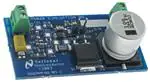
AN-1326 LM5068 Evaluation Board
1
Introduction
The LM5068 evaluation board is designed to provide the design engineer with a fully functional hot-swap
controller board to evaluate the performance of LM5068 hot-swap controller IC, in a typical environment.
The evaluation board is designed using the LM5068-2 (active high Power Good and Fault auto retry
version). This application report explains the apparatus needed and method of operation to the user of the
evaluation board. The LM5068 Negative Voltage Hot Swap Controller (SNVS254) should be consulted in
conjunction with this user's guide.
The performance of the evaluation board is:
• Input range: -10V to -90V
• Transient voltage rating : -100V (absolute maximum)
• Maximum continuous load current: 1.0A
• Maximum short-circuit current : 2.4A
• Board Size: 58.5 mm × 31.8mm
2
Theory of Operation
The LM5068 features all of the functions needed to implement hot-swap capability and intelligent control
of power supply connections during the insertion and removal of circuit cards powered by live system
backplanes as shown in Figure 1.
PLUG-IN BOARD
+
LIVE
BACKPLANE
LM5068
CL
DC-DC
CONVERTER
VDD (GND)
VEE (-48V)
Figure 1. Live System Backplanes
The LM5068 provides both inrush current control and minimizes power supply transients in the backplane
caused by the insertion of additional circuit cards. Once the turn-on sequence is completed, the LM5068
monitors the load current and provides overload protection. The LM5068 controls the external N-Channel
MOSFET to provide programmable load current limiting and circuit breaker functions using a single
external current sense resistor.
The LM5068 issues a power good (PWRGD) signal at the conclusion of a successful power-on sequence.
Input over-voltage or under-voltage fault conditions will cancel the PWRGD indication. The LM5068-1 and
-2 indicate power good as an open-drain active high PWRGD state. The LM5068-3 and -4 indicate power
good as an open-drain active low PWRGD state. The LM5068 is available in MSOP-8 package.
The evaluation board schematic is shown in Figure 2.
All trademarks are the property of their respective owners.
SNVA089A – May 2004 – Revised May 2013
Submit Documentation Feedback
AN-1326 LM5068 Evaluation Board
Copyright © 2004–2013, Texas Instruments Incorporated
1
�Theory of Operation
www.ti.com
GND
GND
J1
J2
-48V
TP8
UV/OV
TP1
VDD
R10
499:
R1
0:
R5
100k:
+
C5
100PF
+
-48V
C6
0.1PF
TP4
UV
R2
100k:
VEE
U1
TP5
OV
R3
4.02k:
VDD
8
OV
TIMER
7
UV
GATE
6
SENSE
5
1
PWRGD
2
3
TP6
TIMER
+
R4
3.40k:
4
C2
NOT USED
+
VEE
R9
0:
+
TP7
GATE
LM5068
C1
NOT USED
C4
0.33PF
VEE
+
R6
0:
C3
22nF
Q1
SUB85N10-10
R7
50m: :
F1
10A
TP2
VEE
R8
0:
TP3
SENSE
Figure 2. Evaluation Board Schematic
The apparatus required to test the evaluation board is:
• 100V/ 5A DC power supply
• 2 or 4 channel analog or digital storage oscilloscope
• Two RMS voltmeters (DVM) with floating inputs
Care must be exercised while operating at high input voltages.
2
AN-1326 LM5068 Evaluation Board
SNVA089A – May 2004 – Revised May 2013
Submit Documentation Feedback
Copyright © 2004–2013, Texas Instruments Incorporated
�Operational Description of the Evaluation Board
www.ti.com
3
Operational Description of the Evaluation Board
The operation of LM5068 hot-swap controller embedded on a plug-in board can be categorized into three
parts:
• Start-up and inrush current limiting
• Auto retry following the detection of a fault
• Load disconnect and power limiting during fault
3.1
Start-up and Inrush Current Limit
Whenever a circuit card with large electrolytic capacitors is inserted into a live backplane, large inrush
currents will occur. These surge currents can cause the backplane voltage to drop, which can reset or
otherwise interfere with adjacent boards. The current surges can also affect connector pins, burn out PCB
traces and can interfere with data by generating EMI. The LM5068 actively limits inrush currents, which
limits load voltage slew rate (ΔV/Δt). The LM5068 has active current limiting threshold of 100mV, and an
RSENSE equal to 50mΩ, therefore the maximum current is limited to 2.0A (see Figure 3).
1
2 ms
2.00V
5.06V
1
2
2 ms
20.0V
50.6V
2
3
2 ms
0.50A
1.26A
3
4
2 ms
5.0V
12.6V
4
CH1: Timer Pin Voltage
CH2: Voltage Across MOSFET Switch
CH3: Load Current
CH4: Gate Voltage
Figure 3. Start-Up Characteristics
3.2
Auto Retry During Faults
If the fault conditions persist long enough for TIMER pin to charge CT to 4V, the LM5068 latches off
(LM5068-1, -3) or switches off and initiates the re-try timer (LM5068-2, -4).
The LM5068-1 and LM5068-3 remains off until the controller is reset by either temporarily pulling the UV
pin low, pulling the TIMER pin below 1 volt, or decreasing the input voltage below the internal VDD undervoltage lockout (UVLO) threshold.
The LM5068-2 and LM5068-4 respond to a fault condition by pulling the GATE and TIMER pins low and
then initiating a timer sequence for automatic re-try. The re-try timer sequence begins with CT capacitor
being charged slowly to 4V with a 6µA current source and then discharged quickly to 1V with a 30mA
discharge current. After eight charge/discharge cycles the GATE pin is released and charged with a 60µA
current source. If the fault condition persists, the LM5068 will again turn off the MOSFET and another 8cycle fault timer sequence will begin.
The Evaluation board is provided with a LM5068-2 , which features the auto retry following a fault
detection (see Figure 4).
SNVA089A – May 2004 – Revised May 2013
Submit Documentation Feedback
AN-1326 LM5068 Evaluation Board
Copyright © 2004–2013, Texas Instruments Incorporated
3
�Operational Description of the Evaluation Board
www.ti.com
1
0.2 s
2.00V
3.10V
1
2
0.2 s
2.00V
3.10V
2
3
0.2 s
0.50A
0.77A
3
4
0.2 s
50V
77V
4
CH1: Timer Pin Voltage
CH2: Gate Pin Voltage
CH3: Current Through MOSFET
CH4: Voltage Across MOSFET
Figure 4. Auto Retry Feature after Fault Detection
3.3
Load Disconnect and Power Limit During Catastrophic Faults
During catastrophic faults like short-circuit on the output when the series MOSFET is fully enhanced, high
inrush currents are still possible. To prevent these high surge currents, the LM5068 has a fast current limit
threshold of 200mV. Fast Discharge Current (FDC) responds to fast rising over-loads such as short circuit
faults. During a short circuit event the fast rising current may overshoot past the ACL (active current limit)
threshold of 100mV due to the finite response time of the ACL loop. If the SENSE voltage reaches 200mV
a fast discharge comparator quickly pulls GATE pin low. The rapid response of the FDC circuit assures a
fast and safe transition to the ACL mode.
The LM5068 circuit breaker action filters low duty cycle over-load conditions to avoid declaring a fault
during short duration load transients. The timer charges capacitor CT with 240µA when the SENSE voltage
is greater than 50mV. When the SENSE pin voltage falls below 50mV, a 6µA current discharges the
TIMER capacitor. Repetitive over-current faults with duty cycle greater than 2.5% will eventually charge
CT and trip the fault timer. This feature protects the pass MOSFET, which has a fast heating and slow
cooling characteristic.
1
1 ms
2.00V
3.10V
1
2
1 ms
5.0V
7.7V
3
2
1 ms
2.00A
3.10A
3
4
1 ms
50V
77V
4
CH1: Timer Pin Voltage
CH2: Gate Pin Voltage
CH3: Current Through MOSFET
CH4: Voltage Across MOSFET
Figure 5. Fast Response Circuit Breaker during Output Short Circuit
4
AN-1326 LM5068 Evaluation Board
SNVA089A – May 2004 – Revised May 2013
Submit Documentation Feedback
Copyright © 2004–2013, Texas Instruments Incorporated
�Conclusion
www.ti.com
4
Conclusion
This user's guide explains the apparatus and method needed to operate the LM5068 evaluation board in a
typical environment. Typical operating modes have been explained with reference to the evaluation board.
5
Component List
Part
Value
C1
NOT USED
Package
Description
Part Number
C2
NOT USED
C3
C4
0.022µF/ 50V
C0805
CAPACITOR, CERAMIC,KEMET
C0805C223K5RAC
0.33µF / 50V
C0805
CAPACITOR,CERAMIC,KEMET
C5
100µF / 100V
C0805C334K5RAC
CAPACITOR, ALUMINIUM
ELECTROLYTIC, SURFACE
MOUNT,PANASONIC
EEV-FK2A101M
C6
0.1µF / 100V
C1206
CAPACITOR, CERAMIC, TDK
C3216X7R2A104KT
F1
10A FUSE
SMD_FUSE
COOPER BUSSMAN FAST
ACTING FUSE TRON
TR/SFT-10 ( Digikey #
283-2439-2-ND)
J1
PCB terminal Blocks/ 10A
MOUSER TERMINAL BLOCKS
651-1727010
J2
PCB terminal Blocks/ 10A
MOUSER TERMINAL BLOCKS
651-1727010
Q1
100V / 60A
N-Channel Power
MOSFET,TO263
VISHAY
SUB85N10-10
R1
0
R1206
SMD RESISTOR, 1% TOL
CRCW12060000F
R2
100k
R1206
SMD RESISTOR, 1% TOL
CRCW12061003F
R3
4.02k
R0805
SMD RESISTOR, 1% TOL
CRCW08054020F
R4
3.40k
R0805
SMD RESISTOR, 1% TOL
CRCW08053401F
R5
100k
R0805
SMD RESISTOR, 1% TOL
CRCW08051003F
R6
0
R0805
SMD RESISTOR, 1% TOL
CRCW08050000F
R7
50m
R2512
SMD RESISTOR, 1% TOL
WSL-2512 .050F
R8
0
R1206
SMD RESISTOR, 1% TOL
CRCW12060000F
R9
0
R1206
SMD RESISTOR, 1% TOL
CRCW12060000F
R10
499
R1206
SMD RESISTOR, 1% TOL
CRCW1206499RF
U1
LM5068
VSSOP-8
Texas Instruments
LM5068-2
SNVA089A – May 2004 – Revised May 2013
Submit Documentation Feedback
AN-1326 LM5068 Evaluation Board
Copyright © 2004–2013, Texas Instruments Incorporated
5
�PCB Layouts
6
www.ti.com
PCB Layouts
Figure 6. Silkscreen Layer as viewed from Top
Figure 7. Top Side Soldermask as viewed from Top
Figure 8. Top (Component) Layer as viewed from Top Figure 9. Bottom Side Soldermask as viewed from Top
Figure 10. Bottom (Solder) Layer as viewed from Top
6
AN-1326 LM5068 Evaluation Board
SNVA089A – May 2004 – Revised May 2013
Submit Documentation Feedback
Copyright © 2004–2013, Texas Instruments Incorporated
�IMPORTANT NOTICE
Texas Instruments Incorporated and its subsidiaries (TI) reserve the right to make corrections, enhancements, improvements and other
changes to its semiconductor products and services per JESD46, latest issue, and to discontinue any product or service per JESD48, latest
issue. Buyers should obtain the latest relevant information before placing orders and should verify that such information is current and
complete. All semiconductor products (also referred to herein as “components”) are sold subject to TI’s terms and conditions of sale
supplied at the time of order acknowledgment.
TI warrants performance of its components to the specifications applicable at the time of sale, in accordance with the warranty in TI’s terms
and conditions of sale of semiconductor products. Testing and other quality control techniques are used to the extent TI deems necessary
to support this warranty. Except where mandated by applicable law, testing of all parameters of each component is not necessarily
performed.
TI assumes no liability for applications assistance or the design of Buyers’ products. Buyers are responsible for their products and
applications using TI components. To minimize the risks associated with Buyers’ products and applications, Buyers should provide
adequate design and operating safeguards.
TI does not warrant or represent that any license, either express or implied, is granted under any patent right, copyright, mask work right, or
other intellectual property right relating to any combination, machine, or process in which TI components or services are used. Information
published by TI regarding third-party products or services does not constitute a license to use such products or services or a warranty or
endorsement thereof. Use of such information may require a license from a third party under the patents or other intellectual property of the
third party, or a license from TI under the patents or other intellectual property of TI.
Reproduction of significant portions of TI information in TI data books or data sheets is permissible only if reproduction is without alteration
and is accompanied by all associated warranties, conditions, limitations, and notices. TI is not responsible or liable for such altered
documentation. Information of third parties may be subject to additional restrictions.
Resale of TI components or services with statements different from or beyond the parameters stated by TI for that component or service
voids all express and any implied warranties for the associated TI component or service and is an unfair and deceptive business practice.
TI is not responsible or liable for any such statements.
Buyer acknowledges and agrees that it is solely responsible for compliance with all legal, regulatory and safety-related requirements
concerning its products, and any use of TI components in its applications, notwithstanding any applications-related information or support
that may be provided by TI. Buyer represents and agrees that it has all the necessary expertise to create and implement safeguards which
anticipate dangerous consequences of failures, monitor failures and their consequences, lessen the likelihood of failures that might cause
harm and take appropriate remedial actions. Buyer will fully indemnify TI and its representatives against any damages arising out of the use
of any TI components in safety-critical applications.
In some cases, TI components may be promoted specifically to facilitate safety-related applications. With such components, TI’s goal is to
help enable customers to design and create their own end-product solutions that meet applicable functional safety standards and
requirements. Nonetheless, such components are subject to these terms.
No TI components are authorized for use in FDA Class III (or similar life-critical medical equipment) unless authorized officers of the parties
have executed a special agreement specifically governing such use.
Only those TI components which TI has specifically designated as military grade or “enhanced plastic” are designed and intended for use in
military/aerospace applications or environments. Buyer acknowledges and agrees that any military or aerospace use of TI components
which have not been so designated is solely at the Buyer's risk, and that Buyer is solely responsible for compliance with all legal and
regulatory requirements in connection with such use.
TI has specifically designated certain components as meeting ISO/TS16949 requirements, mainly for automotive use. In any case of use of
non-designated products, TI will not be responsible for any failure to meet ISO/TS16949.
Products
Applications
Audio
www.ti.com/audio
Automotive and Transportation
www.ti.com/automotive
Amplifiers
amplifier.ti.com
Communications and Telecom
www.ti.com/communications
Data Converters
dataconverter.ti.com
Computers and Peripherals
www.ti.com/computers
DLP® Products
www.dlp.com
Consumer Electronics
www.ti.com/consumer-apps
DSP
dsp.ti.com
Energy and Lighting
www.ti.com/energy
Clocks and Timers
www.ti.com/clocks
Industrial
www.ti.com/industrial
Interface
interface.ti.com
Medical
www.ti.com/medical
Logic
logic.ti.com
Security
www.ti.com/security
Power Mgmt
power.ti.com
Space, Avionics and Defense
www.ti.com/space-avionics-defense
Microcontrollers
microcontroller.ti.com
Video and Imaging
www.ti.com/video
RFID
www.ti-rfid.com
OMAP Applications Processors
www.ti.com/omap
TI E2E Community
e2e.ti.com
Wireless Connectivity
www.ti.com/wirelessconnectivity
Mailing Address: Texas Instruments, Post Office Box 655303, Dallas, Texas 75265
Copyright © 2013, Texas Instruments Incorporated
�