LM5109
LM5109 100V / 1A Peak Half Bridge Gate Driver
Literature Number: SNVS369
�LM5109
100V / 1A Peak Half Bridge Gate Driver
General Description
The LM5109 is a low cost high voltage gate driver, designed
to drive both the high side and the low side N-Channel
MOSFETs in a synchronous buck or a half bridge configuration. The floating high-side driver is capable of working with
rail voltages up to 100V. The outputs are independently
controlled with TTL compatible input thresholds. A robust
level shifter technology operates at high speed while consuming low power and providing clean level transitions from
the control input logic to the high side gate driver. Undervoltage lockout is provided on both the low side and the high
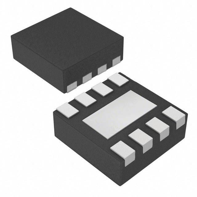
side power rails. The device is available in the SOIC-8 and
the thermally enhanced LLP-8 packages.
Features
n Drives both a high side and low side N-Channel
MOSFET
n 1A peak output current (1.0A sink / 1.0A source)
n Independent TTL compatible inputs
n
n
n
n
n
n
n
Bootstrap supply voltage to 118V DC
Fast propagation times (27 ns typical)
Drives 1000 pF load with 15ns rise and fall times
Excellent propagation delay matching (2 ns typical)
Supply rail under-voltage lockout
Low power consumption
Pin compatible with ISL6700
Typical Applications
n
n
n
n
Current Fed push-pull converters
Half and Full Bridge power converters
Solid state motor drives
Two switch forward power converters
Package
n SOIC-8
n LLP-8 (4 mm x 4 mm)
Simplified Block Diagram
20150501
FIGURE 1.
© 2005 National Semiconductor Corporation
DS201505
www.national.com
LM5109 100V / 1A Peak Half Bridge Gate Driver
April 2005
�LM5109
Connection Diagrams
20150502
20150503
FIGURE 2.
Ordering Information
Ordering Number
Package Type
NSC Package Drawing
LM5109MA
SOIC-8
M08A
Supplied As
LM5109MAX
SOIC-8
M08A
2500 shipped as Tape & Reel
LM5109SD
LLP-8
SDC08A
1000 shipped as Tape & Reel
LM5109SDX
LLP-8
SDC08A
4500 shipped as Tape & Reel
Shipped in anti static rails
Pin Description
Pin #
Name
Description
Application Information
SO-8
LLP-8
1
1
VDD
Positive gate drive supply
Locally decouple to VSS using low ESR/ESL capacitor located
as close to IC as possible.
2
2
HI
High side control input
The LM5109 HI input is compatible with TTL input thresholds.
Unused HI input should be tied to ground and not left open
3
3
LI
Low side control input
The LM5109 LI input is compatible with TTL input thresholds.
Unused LI input should be tied to ground and not left open.
4
4
VSS
Ground reference
All signals are referenced to this ground.
5
5
LO
Low side gate driver output
Connect to the gate of the low side N-MOS device.
6
6
HS
High side source connection
Connect to the negative terminal of the bootstrap capacitor
and to the source of the high side N-MOS device.
7
7
HO
High side gate driver output
Connect to the gate of the low side N-MOS device.
8
8
HB
High side gate driver positive
supply rail
Connect the positive terminal of the bootstrap capacitor to HB
and the negative terminal of the bootstrap capacitor to HS.
The bootstrap capacitor should be placed as close to IC as
possible.
Note: For LLP-8 package it is recommended that the exposed pad on the bottom of the LM5109 be soldered to ground plane on the PCB board and the
ground plane should extend out from underneath the package to improve heat dissipation.
www.national.com
2
�Storage Temperature Range
If Military/Aerospace specified devices are required,
please contact the National Semiconductor Sales Office/
Distributors for availability and specifications.
ESD Rating HBM (Note 2)
VDD to VSS
−0.3V to 18V
LI or HI to VSS
−0.3V to VDD +0.3V
LO to VSS
−0.3V to VDD +0.3V
HO to VSS
VHS −0.3V to VHB +0.3V
HS to VSS (Note 6)
VDD
HB to VSS
8V to 14V
HS (Note 6)
−1V to 100V
HB
VHS +8V to VHS +14V
< 50 V/ns
HS Slew Rate
−5V to 100V
Junction Temperature
118V
Junction Temperature
2 kV
Recommended Operating
Conditions
-0.3V to 18V
HB to HS
−55˚C to +150˚C
−40˚C to +125˚C
-40˚C to +150˚C
Electrical Characteristics
Specifications in standard typeface are for TJ = +25˚C, and those in boldface type apply over the full operating junction temperature range. Unless otherwise specified, VDD = VHB = 12V, VSS = VHS = 0V, No Load on LO or HO .
Symbol
Parameter
Conditions
Min
Typ
Max
Units
0.3
0.6
mA
SUPPLY CURRENTS
IDD
VDD Quiescent Current
IDDO
VDD Operating Current
f = 500 kHz
2.1
3.4
mA
IHB
Total HB Quiescent Current
LI = HI = 0V
0.06
0.2
mA
IHBO
Total HB Operating Current
f = 500 kHz
1.6
3.0
mA
IHBS
HB to VSS Current, Quiescent
VHS = VHB = 100V
0.1
10
IHBSO
HB to VSS Current, Operating
f = 500 kHz
0.5
mA
0.8
1.8
V
1.8
2.2
V
100
180
500
kΩ
6.9
7.4
LI = HI = 0V
µA
INPUT PINS LI and HI
VIL
Low Level Input Voltage Threshold
VIH
High Level Input Voltage Threshold
RI
Input Pulldown Resistance
UNDER VOLTAGE PROTECTION
VDDR
VDD Rising Threshold
VDDH
VDD Threshold Hysteresis
VHBR
HB Rising Threshold
VHBH
HB Threshold Hysteresis
VDDR = VDD - VSS
6.0
0.5
VHBR = VHB - VHS
5.7
6.6
V
V
7.1
0.4
V
V
LO GATE DRIVER
VOLL
Low-Level Output Voltage
ILO = 100 mA
VOHL = VLO – VSS
0.28
0.45
V
VOHL
High-Level Output Voltage
ILO = −100 mA,
VOHL = VDD– VLO
0.45
0.75
V
IOHL
Peak Pullup Current
VLO = 0V
1.0
A
IOLL
Peak Pulldown Current
VLO = 12V
1.0
A
HO GATE DRIVER
VOLH
Low-Level Output Voltage
IHO = 100 mA
VOLH = VHO– VHS
0.28
0.45
V
VOHH
High-Level Output Voltage
IHO = −100 mA
VOHH = VHB– VHO
0.45
0.75
V
IOHH
Peak Pullup Current
VHO = 0V
1.0
A
IOLH
Peak Pulldown Current
VHO = 12V
1.0
A
SOIC-8
160
LLP-8 (Note 3)
40
THERMAL RESISTANCE
θJA
Junction to Ambient
3
˚C/W
www.national.com
LM5109
Absolute Maximum Ratings (Note 1)
�LM5109
Switching Characteristics
Specifications in standard typeface are for TJ = +25˚C, and those in boldface type apply over the full operating junction temperature range. Unless otherwise specified, VDD = VHB = 12V, VSS = VHS = 0V, No Load on LO or HO.
Symbol
Parameter
Conditions
Min
Typ
Max
Units
LM5109
tLPHL
Lower Turn-Off Propagation Delay (LI
Falling to LO Falling)
27
56
ns
tHPHL
Upper Turn-Off Propagation Delay (HI
Falling to HO Falling)
27
56
ns
tLPLH
Lower Turn-On Propagation Delay (LI
Rising to LO Rising)
29
56
ns
tHPLH
Upper Turn-On Propagation Delay (HI
Rising to HO Rising)
29
56
ns
tMON
Delay Matching: Lower Turn-On and
Upper Turn-Off
2
15
ns
tMOFF
Delay Matching: Lower Turn-Off and
Upper Turn-On
2
15
ns
tRC, tFC
Either Output Rise/Fall Time
15
-
ns
tPW
Minimum Input Pulse Width that
Changes the Output
CL = 1000 pF
50
ns
Note 1: Absolute Maximum Ratings indicate limits beyond which damage to the component may occur. Operating Ratings are conditions under which operation of
the device is guaranteed. Operating Ratings do not imply guaranteed performance limits. For guaranteed performance limits and associated test conditions, see the
Electrical Characteristics tables.
Note 2: The human body model is a 100 pF capacitor discharged through a 1.5kΩ resistor into each pin. Pin 6 , Pin 7 and Pin 8 are rated at 500V.
Note 3: 4 layer board with Cu finished thickness 1.5/1/1/1.5 oz. Maximum die size used. 5x body length of Cu trace on PCB top. 50 x 50mm ground and power
planes embedded in PCB. See Application Note AN-1187.
Note 4: Min and Max limits are 100% production tested at 25˚C. Limits over the operating temperature range are guaranteed through correlation using Statistical
Quality Control (SQC) methods. Limits are used to calculate National’s Average Outgoing Quality Level (AOQL).
Note 5: The θJA is not a constant for the package and depends on the printed circuit board design and the operating conditions.
Note 6: In the application the HS node is clamped by the body diode of the external lower N-MOSFET, therefore the HS voltage will generally not exceed -1V.
However in some applications, board resistance and inductance may result in the HS node exceeding this stated voltage transiently.
If negative transients occur on HS, the HS voltage must never be more negative than VDD - 15V. For example, if VDD = 10V, the negative transients at HS must not
exceed -5V.
www.national.com
4
�LM5109
Typical performance Characteristics
VDD Operating Current vs Frequency
HB Operating Current vs Frequency
20150504
20150505
Operating Current vs Temperature
Quiescent Current vs Temperature
20150506
20150507
Quiescent Current vs Voltage
Propagation Delay vs Temperature
20150509
20150508
5
www.national.com
�LM5109
Typical performance Characteristics
(Continued)
LO and HO High Level Output Voltage vs Temperature
LO and HO Low Level Output Voltage vs Temperature
20150510
20150511
Undervoltage Rising Thresholds vs Temperature
Undervoltage Hysteresis vs Temperature
20150514
20150515
Input Thresholds vs Temperature
Input Thresholds vs Supply Voltage
20150517
20150516
www.national.com
6
�LM5109
Timing Diagram
20150518
FIGURE 3.
peak current. Minimizing this loop length and area on the
circuit board is important to ensure reliable operation.
Layout Considerations
The optimum performance of high and low side gate drivers
cannot be achieved without taking due considerations during
circuit board layout. Following points are emphasized.
1. A low ESR / ESL capacitor must be connected close to
the IC, and between VDD and VSS pins and between HB
and HS pins to support high peak currents being drawn
from VDD during turn-on of the external MOSFET.
2. To prevent large voltage transients at the drain of the top
MOSFET, a low ESR electrolytic capacitor must be connected between MOSFET drain and ground (VSS).
3. In order to avoid large negative transients on the switch
node (HS) pin, the parasitic inductances in the source of
top MOSFET and in the drain of the bottom MOSFET
(synchronous rectifier) must be minimized.
4. Grounding Considerations:
a) The first priority in designing grounding connections
is to confine the high peak currents from charging and
discharging the MOSFET gate in a minimal physical
area. This will decrease the loop inductance and minimize noise issues on the gate terminal of the MOSFET.
The MOSFETs should be placed as close as possible to
the gate driver.
b) The second high current path includes the bootstrap capacitor, the bootstrap diode, the local ground
referenced bypass capacitor and low side MOSFET
body diode. The bootstrap capacitor is recharged on the
cycle-by-cycle basis through the bootstrap diode from
the ground referenced VDD bypass capacitor. The recharging occurs in a short time interval and involves high
HS Transient Voltages Below
Ground
The HS node will always be clamped by the body diode of
the lower external FET. In some situations, board resistances and inductances can cause the HS node to transiently swing several volts below ground. The HS node can
swing below ground provided:
1. HS must always be at a lower potential than HO. Pulling
HO more than -0.3V below HS can activate parasitic
transistors resulting in excessive current to flow from the
HB supply possibly resulting in damage to the IC. The
same relationship is true with LO and VSS. If necessary,
a Schottky diode can be placed externally between HO
and HS or LO and GND to protect the IC from this type
of transient. The diode must be placed as close to the IC
pins as possible in order to be effective.
2. HB to HS operating voltage should be 15V or less .
Hence, if the HS pin transient voltage is -5V, VDD should
be ideally limited to 10V to keep HB to HS below 15V.
3. A low ESR bypass capacitor between HB to HS as well
as VDD to VSS is essential for proper operation. The
capacitor should be located at the leads of the IC to
minimize series inductance. The peak currents from LO
and HO can be quite large. Any series inductances with
the bypass capacitor will cause voltage ringing at the
leads of the IC which must be avoided for reliable
operation.
7
www.national.com
�LM5109
Physical Dimensions
inches (millimeters) unless otherwise noted
Controlling dimension is inch. Values in [ ] are millimeters.
Notes: Unless otherwise specified.
1.
2.
3.
Standard lead finish to be 200 microinches/5.08 micrometers minimum lead/tin (solder) on copper.
Dimension does not include mold flash.
Reference JEDEC registration MS-012, Variation AA, dated May 1990.
SOIC-8 Outline Drawing
NS Package Number M08A
www.national.com
8
�inches (millimeters) unless otherwise noted (Continued)
Notes: Unless otherwise specified.
1.
For solder thickness and composition, see “Solder Information” in the packaging section of the National Semiconductor web
page (www.national.com).
2.
3.
Maximum allowable metal burr on lead tips at the package edges is 76 microns.
No JEDEC registration as of May 2003.
LLP-8 Outline Drawing
NS Package Number SDC08A
National does not assume any responsibility for use of any circuitry described, no circuit patent licenses are implied and National reserves
the right at any time without notice to change said circuitry and specifications.
For the most current product information visit us at www.national.com.
LIFE SUPPORT POLICY
NATIONAL’S PRODUCTS ARE NOT AUTHORIZED FOR USE AS CRITICAL COMPONENTS IN LIFE SUPPORT DEVICES OR SYSTEMS
WITHOUT THE EXPRESS WRITTEN APPROVAL OF THE PRESIDENT AND GENERAL COUNSEL OF NATIONAL SEMICONDUCTOR
CORPORATION. As used herein:
1. Life support devices or systems are devices or systems
which, (a) are intended for surgical implant into the body, or
(b) support or sustain life, and whose failure to perform when
properly used in accordance with instructions for use
provided in the labeling, can be reasonably expected to result
in a significant injury to the user.
2. A critical component is any component of a life support
device or system whose failure to perform can be reasonably
expected to cause the failure of the life support device or
system, or to affect its safety or effectiveness.
BANNED SUBSTANCE COMPLIANCE
National Semiconductor manufactures products and uses packing materials that meet the provisions of the Customer Products
Stewardship Specification (CSP-9-111C2) and the Banned Substances and Materials of Interest Specification (CSP-9-111S2) and contain
no ‘‘Banned Substances’’ as defined in CSP-9-111S2.
National Semiconductor
Americas Customer
Support Center
Email: new.feedback@nsc.com
Tel: 1-800-272-9959
www.national.com
National Semiconductor
Europe Customer Support Center
Fax: +49 (0) 180-530 85 86
Email: europe.support@nsc.com
Deutsch Tel: +49 (0) 69 9508 6208
English Tel: +44 (0) 870 24 0 2171
Français Tel: +33 (0) 1 41 91 8790
National Semiconductor
Asia Pacific Customer
Support Center
Email: ap.support@nsc.com
National Semiconductor
Japan Customer Support Center
Fax: 81-3-5639-7507
Email: jpn.feedback@nsc.com
Tel: 81-3-5639-7560
LM5109 100V / 1A Peak Half Bridge Gate Driver
Physical Dimensions
�IMPORTANT NOTICE
Texas Instruments Incorporated and its subsidiaries (TI) reserve the right to make corrections, modifications, enhancements, improvements,
and other changes to its products and services at any time and to discontinue any product or service without notice. Customers should
obtain the latest relevant information before placing orders and should verify that such information is current and complete. All products are
sold subject to TI’s terms and conditions of sale supplied at the time of order acknowledgment.
TI warrants performance of its hardware products to the specifications applicable at the time of sale in accordance with TI’s standard
warranty. Testing and other quality control techniques are used to the extent TI deems necessary to support this warranty. Except where
mandated by government requirements, testing of all parameters of each product is not necessarily performed.
TI assumes no liability for applications assistance or customer product design. Customers are responsible for their products and
applications using TI components. To minimize the risks associated with customer products and applications, customers should provide
adequate design and operating safeguards.
TI does not warrant or represent that any license, either express or implied, is granted under any TI patent right, copyright, mask work right,
or other TI intellectual property right relating to any combination, machine, or process in which TI products or services are used. Information
published by TI regarding third-party products or services does not constitute a license from TI to use such products or services or a
warranty or endorsement thereof. Use of such information may require a license from a third party under the patents or other intellectual
property of the third party, or a license from TI under the patents or other intellectual property of TI.
Reproduction of TI information in TI data books or data sheets is permissible only if reproduction is without alteration and is accompanied
by all associated warranties, conditions, limitations, and notices. Reproduction of this information with alteration is an unfair and deceptive
business practice. TI is not responsible or liable for such altered documentation. Information of third parties may be subject to additional
restrictions.
Resale of TI products or services with statements different from or beyond the parameters stated by TI for that product or service voids all
express and any implied warranties for the associated TI product or service and is an unfair and deceptive business practice. TI is not
responsible or liable for any such statements.
TI products are not authorized for use in safety-critical applications (such as life support) where a failure of the TI product would reasonably
be expected to cause severe personal injury or death, unless officers of the parties have executed an agreement specifically governing
such use. Buyers represent that they have all necessary expertise in the safety and regulatory ramifications of their applications, and
acknowledge and agree that they are solely responsible for all legal, regulatory and safety-related requirements concerning their products
and any use of TI products in such safety-critical applications, notwithstanding any applications-related information or support that may be
provided by TI. Further, Buyers must fully indemnify TI and its representatives against any damages arising out of the use of TI products in
such safety-critical applications.
TI products are neither designed nor intended for use in military/aerospace applications or environments unless the TI products are
specifically designated by TI as military-grade or "enhanced plastic." Only products designated by TI as military-grade meet military
specifications. Buyers acknowledge and agree that any such use of TI products which TI has not designated as military-grade is solely at
the Buyer's risk, and that they are solely responsible for compliance with all legal and regulatory requirements in connection with such use.
TI products are neither designed nor intended for use in automotive applications or environments unless the specific TI products are
designated by TI as compliant with ISO/TS 16949 requirements. Buyers acknowledge and agree that, if they use any non-designated
products in automotive applications, TI will not be responsible for any failure to meet such requirements.
Following are URLs where you can obtain information on other Texas Instruments products and application solutions:
Products
Applications
Audio
www.ti.com/audio
Communications and Telecom www.ti.com/communications
Amplifiers
amplifier.ti.com
Computers and Peripherals
www.ti.com/computers
Data Converters
dataconverter.ti.com
Consumer Electronics
www.ti.com/consumer-apps
DLP® Products
www.dlp.com
Energy and Lighting
www.ti.com/energy
DSP
dsp.ti.com
Industrial
www.ti.com/industrial
Clocks and Timers
www.ti.com/clocks
Medical
www.ti.com/medical
Interface
interface.ti.com
Security
www.ti.com/security
Logic
logic.ti.com
Space, Avionics and Defense
www.ti.com/space-avionics-defense
Power Mgmt
power.ti.com
Transportation and Automotive www.ti.com/automotive
Microcontrollers
microcontroller.ti.com
Video and Imaging
RFID
www.ti-rfid.com
OMAP Mobile Processors
www.ti.com/omap
Wireless Connectivity
www.ti.com/wirelessconnectivity
TI E2E Community Home Page
www.ti.com/video
e2e.ti.com
Mailing Address: Texas Instruments, Post Office Box 655303, Dallas, Texas 75265
Copyright © 2011, Texas Instruments Incorporated
�


 工商网监
湘ICP备2023018690号
工商网监
湘ICP备2023018690号
