Sample &
Buy
Product
Folder
Support &
Community
Tools &
Software
Technical
Documents
LM5114
SNVS790F – JANUARY 2012 – REVISED NOVEMBER 2015
LM5114 Single 7.6-A Peak Current Low-Side Gate Driver
1 Features
3 Description
•
The LM5114 is designed to drive low-side MOSFETs
in boost-type configurations or to drive secondary
synchronous MOSFETs in isolated topologies. With
strong sink current capability, the LM5114 can drive
multiple FETs in parallel. The LM5114 also has the
features necessary to drive low-side enhancement
mode Gallium Nitride (GaN) FETs. The LM5114
provides inverting and noninverting inputs to satisfy
requirements for inverting and Noninverting gate drive
in a single device type. The inputs of the LM5114 are
TTL/CMOS Logic compatible and withstand input
voltages up to 14 V regardless of the VDD voltage.
The LM5114 has split gate outputs, providing
flexibility to adjust the turnon and turnoff strength
independently. The LM5114 has fast switching speed
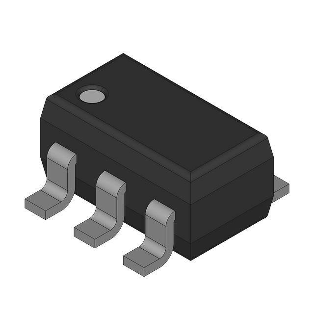
and minimized propagation delays, facilitating highfrequency operation. The LM5114 is available in a 6pin SOT-23 package and a 6-pin WSON package
with an exposed pad to aid thermal dissipation.
1
•
•
•
•
•
•
•
•
•
•
•
•
•
Independent Source and Sink Outputs for
Controllable Rise and Fall Times
4-V to 12.6-V Single Power Supply
7.6-A/1.3-A Peak Sink and Source Drive Current
0.23-Ω Open-drain Pulldown Sink Output
2-Ω Open-drain Pullup Source Output
12-ns (Typical) Propagation Delay
Matching Delay Time Between Inverting and
Noninverting Inputs
TTL/CMOS Logic Inputs
0.68-V Input Hysteresis
Up to 14-V Logic Inputs (Regardless of VDD
Voltage)
Low Input Capacitance: 2.5-pF (Typical)
–40°C to 125°C Operating Temperature Range
Pin-to-Pin Compatible With MAX5048
6-Pin SOT-23
Device Information(1)
PART NUMBER
2 Applications
•
•
•
•
LM5114
Boost Converters
Flyback and Forward Converters
Secondary Synchronous FETs Drive in Isolated
Topologies
Motor Control
PACKAGE
BODY SIZE (NOM)
SOT-23 (6)
2.90 mm × 1.60 mm
WSON (6)
3.00 mm × 3.00 mm
(1) For all available packages, see the orderable addendum at
the end of the data sheet.
Block Diagram
VDD
UVLO
P_OUT
IN
DRIVER
N_OUT
INB
UVLO
Power-off
pull-down
clamp
VSS
1
An IMPORTANT NOTICE at the end of this data sheet addresses availability, warranty, changes, use in safety-critical applications,
intellectual property matters and other important disclaimers. PRODUCTION DATA.
�LM5114
SNVS790F – JANUARY 2012 – REVISED NOVEMBER 2015
www.ti.com
Table of Contents
1
2
3
4
5
6
7
8
Features ..................................................................
Applications ...........................................................
Description .............................................................
Revision History.....................................................
Device Comparison Table.....................................
Pin Configuration and Functions .........................
Specifications.........................................................
1
1
1
2
3
3
4
7.1
7.2
7.3
7.4
7.5
7.6
7.7
4
4
4
4
5
6
8
Absolute Maximum Ratings ......................................
ESD Ratings..............................................................
Recommended Operating Conditions.......................
Thermal Information ..................................................
Electrical Characteristics ..........................................
Switching Characteristics ..........................................
Typical Characteristics ..............................................
Detailed Description ............................................ 12
8.1 Overview ................................................................ 12
8.2 Functional Block Diagram ....................................... 12
8.3 Feature Description ................................................ 12
8.4 Device Functional Modes........................................ 12
9
Application and Implementation ........................ 13
9.1 Application Information............................................ 13
9.2 Typical Application .................................................. 13
9.3 System Examples ................................................... 17
10 Power Supply Recommendations ..................... 18
11 Layout................................................................... 18
11.1 Layout Guidelines ................................................. 18
11.2 Layout Example .................................................... 18
12 Device and Documentation Support ................. 19
12.1
12.2
12.3
12.4
Community Resources..........................................
Trademarks ...........................................................
Electrostatic Discharge Caution ............................
Glossary ................................................................
19
19
19
19
13 Mechanical, Packaging, and Orderable
Information ........................................................... 19
4 Revision History
NOTE: Page numbers for previous revisions may differ from page numbers in the current version.
Changes from Revision E (March 2013) to Revision F
•
Added Pin Configuration and Functions section, ESD Ratings table, Thermal Information table, Feature Description
section, Device Functional Modes, Application and Implementation section, Power Supply Recommendations
section, Layout section, Device and Documentation Support section, and Mechanical, Packaging, and Orderable
Information section ................................................................................................................................................................ 1
Changes from Revision D (August 2012) to Revision E
•
2
Page
Page
Changed layout of National Data Sheet to TI format ........................................................................................................... 18
Submit Documentation Feedback
Copyright © 2012–2015, Texas Instruments Incorporated
Product Folder Links: LM5114
�LM5114
www.ti.com
SNVS790F – JANUARY 2012 – REVISED NOVEMBER 2015
5 Device Comparison Table
BASE PART NUMBER
INPUT THRESHOLDS
LM5114A
CMOS
LM5114B
TTL
6 Pin Configuration and Functions
DBV Package
6-Pin SOT-23
Top View
NGG Package
6-Pin WSON
Top View
VDD
1
6
IN
P_OUT
2
5
N_OUT
3
4
VDD
1
6
IN
INB
P_OUT
2
5
INB
VSS
N_OUT
3
4
VSS
Exposed Pad
Pin Functions
PIN
NAME
I/O
DESCRIPTION
SOT-23
WSON
IN
6
6
I
Noninverting logic input
Connect to VDD when not used.
INB
5
5
I
Inverting logic input
Connect to VSS when not used.
N_OUT
3
3
O
Sink-current output
Connect to the gate of the MOSFET with a short, low inductance path. A gate
resistor can be used to adjust the turnoff speed.
P_OUT
2
2
O
Source-current output
Connect to the gate of the MOSFET with a short, low inductance path. A gate
resistor can be used to adjust the turnon speed.
VDD
1
1
—
Gate drive supply
Locally decouple to VSS using low ESR/ESL capacitor located as close as possible
to the IC.
VSS
4
4
—
Ground
All signals are referenced to this ground.
EP
—
✓
—
It is recommended that the exposed pad on the bottom of the package is soldered to
ground plane on the PC board to aid thermal dissipation.
Submit Documentation Feedback
Copyright © 2012–2015, Texas Instruments Incorporated
Product Folder Links: LM5114
3
�LM5114
SNVS790F – JANUARY 2012 – REVISED NOVEMBER 2015
www.ti.com
7 Specifications
7.1 Absolute Maximum Ratings
over operating free-air temperature range (unless otherwise noted) (1)
MIN
MAX
UNIT
VDD to VSS
−0.3
14
V
IN, INB to VSS
−0.3
14
V
N_OUT to VSS
−0.3
VDD + 0.3
V
P_OUT to VSS
−0.3
VDD + 0.3
V
150
°C
150
°C
Junction temperature
−55
Storage temperature, Tstg
(1)
Stresses beyond those listed under Absolute Maximum Ratings may cause permanent damage to the device. These are stress ratings
only, which do not imply functional operation of the device at these or any other conditions beyond those indicated under Recommended
Operating Conditions. Exposure to absolute-maximum-rated conditions for extended periods may affect device reliability.
7.2 ESD Ratings
V(ESD)
(1)
(2)
Electrostatic discharge
VALUE
UNIT
Human-body model (HBM), per ANSI/ESDA/JEDEC JS-001 (1)
±2000
V
Charged-device model (CDM), per JEDEC specification JESD22C101 (2)
±1000
V
JEDEC document JEP155 states that 500-V HBM allows safe manufacturing with a standard ESD control process.
JEDEC document JEP157 states that 250-V CDM allows safe manufacturing with a standard ESD control process.
7.3 Recommended Operating Conditions
over operating free-air temperature range (unless otherwise noted)
MIN
VDD
Junction temperature
NOM
MAX
UNIT
4
12.6
V
40
125
°C
7.4 Thermal Information
LM5114
THERMAL METRIC (1)
DBV (SOT-23)
NGG (WSON)
UNIT
6 PINS
6 PINS
RθJA
Junction-to-ambient thermal resistance
108.1
51.0
°C/W
RθJC(top)
Junction-to-case (top) thermal resistance
54.2
47.0
°C/W
RθJB
Junction-to-board thermal resistance
24.9
25.3
°C/W
ψJT
Junction-to-top characterization parameter
1.3
0.6
°C/W
ψJB
Junction-to-board characterization parameter
23.9
25.4
°C/W
RθJC(bot)
Junction-to-case (bottom) thermal resistance
NA
5.8
°C/W
(1)
4
For more information about traditional and new thermal metrics, see the Semiconductor and IC Package Thermal Metrics application
report, SPRA953.
Submit Documentation Feedback
Copyright © 2012–2015, Texas Instruments Incorporated
Product Folder Links: LM5114
�LM5114
www.ti.com
SNVS790F – JANUARY 2012 – REVISED NOVEMBER 2015
7.5 Electrical Characteristics
Minimum and Maximum limits are ensured through test, design, or statistical correlation. Typical values represent the most
likely parametric norm at TJ = 25°C, and are provided for reference purposes only. Unless otherwise specified, VDD = 12 V (1).
PARAMETER
TEST CONDITIONS
MIN
TYP
MAX
UNIT
12.6
V
POWER SUPPLY
VDD
VDD operating voltage
UVLO
VDD undervoltage
lockout
(TJ) range of –40°C to 125°C
4.0
TJ = 25°C
VDD Rising
(TJ) range of
–40°C to 125°C
3.6
3.25
VDD undervoltage lockout hysteresis
0.4
TJ = 25°C
IDD
VDD quiescent current
4.00
V
V
0.95
IN = INB = VDD
(TJ) range of
–40°C to 125°C
VDD = 10 V,
IN-OUT = –100 mA
TJ = 25°C
0.23
0.26
Ω
TJ = 125°C
0.38
0.43
Ω
VDD = 4.5 V,
IN-OUT = –100 mA
TJ = 25°C
0.24
0.28
Ω
TJ = 125°C
0.40
0.47
Ω
VDD = 10 V,
IN-OUT = –100 mA
TJ = 25°C
0.31
0.34
Ω
TJ = 125°C
0.46
0.51
Ω
VDD = 4.5 V,
IN-OUT = –100 mA
TJ = 25°C
0.32
0.36
Ω
TJ = 125°C
0.48
0.55
Ω
1.9
mA
N-CHANNEL OUTPUT
RON-N (SOT-23-6)
Driver output
resistance – pulling
down
Driver output
resistance – pulling
down
RON-N (WSON-6)
Power-off pulldown
resistance
VDD = 0 V, IN-OUT = –10 mA
3.3
10
Ω
Power-off pulldown
clamp voltage
VDD = 0 V, IN-OUT = –10 mA
0.85
1.0
V
ILK-N
Output leakage current
N_OUT = VDD
IPK-N
Peak sink current
CL = 10,000 pF
TJ = 25°C
6.85
(TJ) range of
–40°C to 125°C
20
7.6
µA
A
P-CHANNEL OUTPUT
RON-P (SOT-23-6)
RON-P (WSON-6)
Driver output
resistance – pulling up
Driver output
resistance – pulling up
VDD = 10 V,
IP-OUT = 50 mA
TJ = 25°C
2.00
3.00
Ω
TJ = 125°C
2.85
4.30
Ω
VDD = 4.5 V,
IP-OUT = 50 mA
TJ = 25°C
2.20
3.30
Ω
TJ = 125°C
3.10
4.70
Ω
VDD = 10 V,
IP-OUT = 50 mA
TJ = 25°C
2.08
3.08
Ω
TJ = 125°C
2.93
4.38
Ω
VDD = 4.5 V,
IP-OUT = 50 mA
TJ = 25°C
2.28
3.38
Ω
TJ = 125°C
3.18
4.78
Ω
TJ = 25°C
0.001
ILK-P
Output leakage current
P_OUT = 0
IPK-P
Peak source current
CL = 10,000 pF
(TJ) range of
–40°C to 125°C
10
1.3
µA
A
LOGIC INPUT
VIH
Logic 1 input voltage
LM5114A
(TJ) range of
–40°C to 125°C
LM5114B
VIL
Logic 0 input voltage
LM5114A
V
2.4
(TJ) range of
–40°C to 125°C
LM5114B
(1)
0.67 ×
VDD
V
0.33 ×
VDD
V
0.8
V
Min and Max limits are 100% production tested at 25°C. Limits over the operating temperature range are ensured through correlation
using statistical quality control (SQC) methods. Limits are used to calculate TI’s average outgoing quality level (AOQL).
Submit Documentation Feedback
Copyright © 2012–2015, Texas Instruments Incorporated
Product Folder Links: LM5114
5
�LM5114
SNVS790F – JANUARY 2012 – REVISED NOVEMBER 2015
www.ti.com
Electrical Characteristics (continued)
Minimum and Maximum limits are ensured through test, design, or statistical correlation. Typical values represent the most
likely parametric norm at TJ = 25°C, and are provided for reference purposes only. Unless otherwise specified, VDD = 12 V (1).
PARAMETER
TEST CONDITIONS
MIN
TYP
MAX
UNIT
LOGIC INPUT (continued)
Logic-input hysteresis
LM5114A
1.6
V
LM5114B
0.68
V
VHYS
TJ = 25°C
Logic-input current
CIN
INB = VDD or 0
0.001
(TJ) range of
–40°C to 125°C
µA
10
Input capacitance
2.5
pF
7.6 Switching Characteristics
over operating free-air temperature range (unless otherwise noted)
PARAMETER
TEST CONDITIONS
MIN
TYP
MAX
UNIT
POWER SUPPLY
UVLO
VDD undervoltage lockout to output
VDD Rising
delay time
300
ns
CL = 1000 pF
8
ns
CL = 5000 pF
45
ns
CL = 10,000 pF
82
ns
CL = 1000 pF
3.2
ns
CL = 5000 pF
7.5
ns
12.5
ns
SWITCHING CHARACTERISTICS FOR VDD = 10 V
tR
tF
Rise time
Fall time
CL = 10,000 pF
TJ = 25°C
LM5114A
tD-ON
Turnon propagation delay
CL =
1000 pF
12
(TJ) range of
–40°C to 125°C
5
TJ = 25°C
LM5114B
tD-OFF
Turnoff propagation delay
CL =
1000 pF
(TJ) range of
–40°C to 125°C
6
25
12
(TJ) range of
–40°C to 125°C
5
TJ = 25°C
LM5114B
ns
12
TJ = 25°C
LM5114A
30
30
ns
12
(TJ) range of
–40°C to 125°C
6
Break-before-make Time
25
2.5
ns
CL = 1000 pF
12
ns
CL = 5000 pF
41
ns
CL = 10,000 pF
74
ns
CL = 1000 pF
3.0
ns
CL = 5000 pF
7.0
ns
11.3
ns
SWITCHING CHARACTERISTICS FOR VDD = 4.5 V
tR
tF
Rise time
Fall time
CL = 10,000 pF
TJ = 25°C
LM5114A
tD-ON
Turnon propagation delay
CL =
1000 pF
5
TJ = 25°C
LM5114B
6
36
(TJ) range of
–40°C to 125°C
27
(TJ) range of
–40°C to 125°C
Submit Documentation Feedback
17
8
ns
14
Copyright © 2012–2015, Texas Instruments Incorporated
Product Folder Links: LM5114
�LM5114
www.ti.com
SNVS790F – JANUARY 2012 – REVISED NOVEMBER 2015
Switching Characteristics (continued)
over operating free-air temperature range (unless otherwise noted)
PARAMETER
TEST CONDITIONS
MIN
TYP
MAX
UNIT
SWITCHING CHARACTERISTICS FOR VDD = 4.5 V (continued)
TJ = 25°C
LM5114A
tD-OFF
CL =
1000 pF
Turnoff propagation delay
36
(TJ) range of
–40°C to 125°C
5
17
TJ = 25°C
LM5114B
27
(TJ) range of
–40°C to 125°C
Break-before-make time
8
ns
14
4.2
ns
50%
50%
IN
tD-OFF
tD-ON
90%
OUTPUT
10%
tf
tr
50%
50%
INB
tD-ON
tD-OFF
OUTPUT
90%
10%
tf
Note:
tr
P_OUT and N_OUT are tied together.
Figure 1. Timing Diagram
Submit Documentation Feedback
Copyright © 2012–2015, Texas Instruments Incorporated
Product Folder Links: LM5114
7
�LM5114
SNVS790F – JANUARY 2012 – REVISED NOVEMBER 2015
www.ti.com
7.7 Typical Characteristics
8
Figure 2. Source Current vs Output Voltage
Figure 3. Sink Current vs Output Voltage
Figure 4. Peak Source Current vs VDD Voltage
Figure 5. Peak Sink Current vs VDD Voltage
Figure 6. LM5114A Turnon Propagation Delay vs VDD
Figure 7. LM5114A Turnoff Propagation Delay vs VDD
Submit Documentation Feedback
Copyright © 2012–2015, Texas Instruments Incorporated
Product Folder Links: LM5114
�LM5114
www.ti.com
SNVS790F – JANUARY 2012 – REVISED NOVEMBER 2015
Typical Characteristics (continued)
Figure 8. LM5114B Turnon Propagation Delay vs VDD
Figure 9. LM5114B Turnoff Propagation Delay vs VDD
Figure 10. UVLO Threshold vs Temperature
Figure 11. Quiescent Current vs Temperature
Figure 12. Supply Current vs Frequency
Figure 13. Supply Current vs Capacitive Load
Submit Documentation Feedback
Copyright © 2012–2015, Texas Instruments Incorporated
Product Folder Links: LM5114
9
�LM5114
SNVS790F – JANUARY 2012 – REVISED NOVEMBER 2015
www.ti.com
Typical Characteristics (continued)
10
Figure 14. Input Voltage vs Output Voltage
(VDD = 4 V, CL = 5000 pF)
Figure 15. Input Voltage vs Output Voltage
(VDD = 4 V, CL = 5000 pF)
Figure 16. Input Voltage vs Output Voltage
(VDD = 12 V, CL = 5000 pF)
Figure 17. Input Voltage vs Output Voltage
(VDD = 12 V, CL = 5000 pF)
Figure 18. Input Voltage vs Output Voltage
(VDD = 4 V, CL = 10000 pF)
Figure 19. Input Voltage vs Output Voltage
(VDD = 4 V, CL = 10000 pF)
Submit Documentation Feedback
Copyright © 2012–2015, Texas Instruments Incorporated
Product Folder Links: LM5114
�LM5114
www.ti.com
SNVS790F – JANUARY 2012 – REVISED NOVEMBER 2015
Typical Characteristics (continued)
Figure 20. Input Voltage vs Output Voltage
(VDD = 12 V, CL = 10000 pF)
Figure 21. Input Voltage vs Output Voltage
(VDD = 12 V, CL = 10000 pF)
Submit Documentation Feedback
Copyright © 2012–2015, Texas Instruments Incorporated
Product Folder Links: LM5114
11
�LM5114
SNVS790F – JANUARY 2012 – REVISED NOVEMBER 2015
www.ti.com
8 Detailed Description
8.1 Overview
The LM5114 is designed to drive low-side MOSFETs in boost-type configurations or to drive secondary
synchronous MOSFETs in isolated topologies. The LM5114 offers both inverting and Noninverting inputs to
satisfy requirements for inverting and Noninverting gate drive in a single device type.
8.2 Functional Block Diagram
VDD
UVLO
P_OUT
IN
DRIVER
N_OUT
INB
Power-off
pull-down
clamp
UVLO
VSS
8.3 Feature Description
The LM5114 is a single low-side gate driver with 7.6-A/1.3-A peak sink/source drive current capability. Inputs of
the LM5114 are TTL Logic compatible and can withstand the input voltages up to 14-V regardless of the VDD
voltage. This allows inputs of the LM5114 to be connected directly to most PWM controllers. The split outputs of
the LM5114 offer flexibility to adjust the turnon and turnoff speed independently by adding additional impedance
in either the turnon path or the turnoff path.
The LM5114 includes an under-voltage lockout (UVLO) circuit. When the VDD voltage is below the UVLO
threshold voltage, the IN and INB inputs are ignored, and if there is sufficient VDD voltage, the output NMOS is
turned on to pull the N_OUT low. In addition, the LM5114 has an internal PNP transistor in parallel with the
output NMOS. Under the UVLO condition, the PNP transistor will be on and clamp the N_OUT voltage below
1 V.
Under the UVLO condition, the PNP transistor will be on and clamp the N_OUT voltage below 1 V. This feature
ensures the N_OUT remaining low when VDD voltage is not sufficient to enhance the output NMOS. The
LM5114 has the features necessary to drive low-side enhancement mode GaN FETs. Due to the fast switching
speed and relatively low gate voltage of enhancement mode GaN FETs, PCB layout is crucial to achieve reliable
operation. Refer to Layout for details.
8.4 Device Functional Modes
Table 1. Truth Table
IN
12
INB
P_OUT
N_OUT
L
L
OPEN
L
L
H
OPEN
L
H
L
H
OPEN
H
H
OPEN
L
Submit Documentation Feedback
Copyright © 2012–2015, Texas Instruments Incorporated
Product Folder Links: LM5114
�LM5114
www.ti.com
SNVS790F – JANUARY 2012 – REVISED NOVEMBER 2015
9 Application and Implementation
NOTE
Information in the following applications sections is not part of the TI component
specification, and TI does not warrant its accuracy or completeness. TI’s customers are
responsible for determining suitability of components for their purposes. Customers should
validate and test their design implementation to confirm system functionality.
9.1 Application Information
The LM5114 has the features necessary to drive low-side enhancement mode GaN FETs. Due to the fast
switching speed and relatively low gate voltage of enhancement mode GaN FETs, PCB layout is crucial to
achieve reliable operation. Refer to Figure 32 for details.
9.2 Typical Application
Boost DC-DC converter using a 100-V enhancement mode GaN FET (EPC2001) as the boost power switch. The
control circuitry is implemented with the LM5114, a 100-V current mode PWM controller.
VIN
VOUT
VDD
P_OUT
PWM
IN
+
LM5114
N_OUT
INB
VSS
Figure 22. Simplified Boost Converter
Submit Documentation Feedback
Copyright © 2012–2015, Texas Instruments Incorporated
Product Folder Links: LM5114
13
�LM5114
SNVS790F – JANUARY 2012 – REVISED NOVEMBER 2015
www.ti.com
Typical Application (continued)
9.2.1 Design Requirements
See Table 2 for the parameter and values.
Table 2. Operating Parameters
PARAMETER
VALUE
Input Operating Voltage
24 V to 66 V
Output Voltage
75 V
Output Current
2A
Measured Efficiency
97% @ at 48 V 2 A
Frequency of Operation
500 kHz
9.2.1.1 Power Dissipation
It is important to keep the power consumption of the driver below the maximum power dissipation limit of the
package at the operating temperature. The total power dissipation of the LM5114 is the sum of the gate charge
losses and the losses in the driver due to the internal CMOS stages used to buffer the output as well as the
power losses associated with the quiescent current.
The gate charge losses can be calculated with the total input gate charge as in Equation 1 and Equation 2:
(1)
or
where
•
Fsw is switching frequency
(2)
The power dissipation associated with the internal circuit operation of the driver can be estimated with the
characterization curves of the LM5114. For a given ambient temperature, the maximum allowable power loss of
the IC can be defined as Equation 3:
where
•
P is the total power dissipation of the driver
(3)
This power PG is dissipated in the resistive elements of the circuit when the MOSFET/IGBT is being turned on
and off. Half of the total power is dissipated when the load capacitor is charged during turnon, and the other half
is dissipated when the load capacitor is discharged during turnoff. When no external gate resistor is employed
between the driver and MOSFET/IGBT, this power is completely dissipated inside the driver package. With the
use of external gate-drive resistors, the power dissipation is shared between the internal resistance of driver and
external gate resistor.
14
Submit Documentation Feedback
Copyright © 2012–2015, Texas Instruments Incorporated
Product Folder Links: LM5114
�LM5114
www.ti.com
SNVS790F – JANUARY 2012 – REVISED NOVEMBER 2015
9.2.1.1.1 Gate Drive
The enhancement mode GaN FETs have small gate capacitance and low threshold gate voltage. Therefore GaN
FETs are prone to gate oscillations induced by PCB parasitic elements. It is necessary to place the driver as
close to the GaN FET as possible to minimize the stray inductance. Gate resistors can be used to damp the
oscillations and to adjust the switching speed. The LM5114 has split outputs, providing flexibility to adjust the
turnon and turnoff strength independently. In the evaluation board, 1.5-Ω and 2.7-Ω gate resistors are used in the
turnon and turnoff path respectively.
9.2.2 Detailed Design Procedure
The LM5114 has the features necessary to drive low-side enhancement mode GaN FETs. Due to the fast
switching speed and relatively low gate voltage of enhancement mode GaN FETs, PCB layout is crucial to
achieve reliable operation.
Generally, the switching speed of the power switch during turnon and turnoff should be as fast as possible in
order to minimize switching power losses. The gate driver device must be able to provide the required peak
current for achieving the targeted switching speeds with the targeted power switch. The system requirement for
the switching speed is typically described in terms of the slew rate of the drain-to-source voltage of the power
FET (such as dVDS/dt).
For example, the system requirement in this application might state that a EPC2001 GaN FET must be turned on
with a dVDS/dt of 20 V/ns or higher with a DC bus voltage of 75 V.
This requirement means that the entire drain-to-source voltage swing during the FET turnon event (from 75 V in
the OFF state to VDS(on) in on state) must be completed in approximately 3.75 ns or less. When the drain-tosource voltage swing occurs, the Miller charge of the power FET (QGD parameter in EPC2001 data sheet is
2.2 nC typical) is supplied by the peak current of gate driver. To achieve the targeted dVDS/dt, the gate driver
must be capable of providing the QGD charge in 3.75 ns or less. In other words a peak current of 0.586 A
(= 2.2 nC / 2 ns) or higher must be provided by the gate driver.
The LM5114 gate driver is capable of providing 1.3-A peak sourcing current which clearly exceeds the design
requirement and has the capability to meet the switching speed needed. The 2.2x overdrive capability provides
an extra margin against part-to-part variations in the QGD parameter of the power MOSFET along with additional
flexibility to insert external gate resistors and fine tune the switching speed for efficiency versus EMI
optimizations. However, in practical designs the parasitic trace inductance in the gate drive circuit of the PCB will
have a definitive role to play on the FET switching speed.
The effect of this trace inductance is to limit the dI/dt of the output current pulse of the gate driver. In order to
illustrate this, consider output current pulse waveform from the gate driver to be approximated to a triangular
profile, where the area under the triangle (½ × IPEAK × time) would equal the total gate charge of the power FET
(QG parameter in the EPC2001 GaNFET datasheet = 8 nC typical). If the parasitic trace inductance limits the
dI/dt then a situation may occur in which the full peak current capability of the gate driver is not fully achieved in
the time required to deliver the QG required for the GaNFET switching. In other words the time parameter in the
equation would dominate and the IPEAK value of the current pulse would be much less than the true peak
current capability of the device, while the required QG is still delivered.
Because of this, the desired switching speed may not be realized, even when theoretical calculations indicate the
gate driver is capable of achieving the targeted switching speed. Thus, placing the gate driver device very close
to the power FET and designing a tight gate drive-loop with minimal PCB trace inductance is important to realize
the full peak-current capability of the gate driver.
Submit Documentation Feedback
Copyright © 2012–2015, Texas Instruments Incorporated
Product Folder Links: LM5114
15
�LM5114
SNVS790F – JANUARY 2012 – REVISED NOVEMBER 2015
www.ti.com
9.2.3 Application Curves
Conditions:
Input Voltage = 48 VDC, Load Current = 2 A
Traces:
Top Trace: Switch-node voltage, Volt/div = 50 V
Bottom Trace: Gate-Source Voltage of GaN FET, Volt/div = 2 V
Bandwidth Limit = 600 MHz
Horizontal Resolution = 500 ns/div
Figure 23. Gate-Source Voltage
Conditions:
Input Voltage = 24 VDC, Load Current = 2 A
Traces:
Top Trace: Inductor Current, Amp/div = 5 A
Bottom Trace: Switch-Node Voltage, Volt/div = 20 V
Bandwidth Limit = 600 MHz
Horizontal Resolution = 1 µs/div
Figure 24. Switching Node Voltage VIN = 24 V, Load
Current = 2 A
Conditions:
Input Voltage = 48 VDC
Load Current = 2 A
Traces:
Top Trace: Inductor Current, Amps/div = 5 A
Bottom Trace: Switch-Node Voltage, Volt/div = 20 V
Bandwidth Limit = 600 MHz
Horizontal Resolution = 1 µs/div
Figure 25. Switching Node Voltage VIN = 48 V, Load
Current = 2 A
Conditions:
Input Voltage = 66 VDC
Load Current = 2 A
Traces:
Top Trace: Inductor Current, Amp/div = 5 A
Bottom Trace: Switch-Node Voltage, Volt/div = 20 V
Bandwidth Limit = 600 MHz
Horizontal Resolution = 1 µs/div
Figure 26. Switching Node Voltage VIN = 66 V, Load
Current = 2 A
16
Submit Documentation Feedback
Copyright © 2012–2015, Texas Instruments Incorporated
Product Folder Links: LM5114
�LM5114
www.ti.com
SNVS790F – JANUARY 2012 – REVISED NOVEMBER 2015
Figure 27. Input Voltage vs Output Voltage
(VDD = 12 V, CL = 10000 pF)
9.3 System Examples
VDD
VDD
P_OUT
PWM
IN
P_OUT
LM5114
IN
N_OUT
INB
LM5114
N_OUT
PWM
VSS
INB
VSS
Figure 28. Noninverting Application
Figure 29. Inverting Application
VDD
VDD
P_OUT
PWM
EN
IN
P_OUT
EN
LM5114
N_OUT
PWM
INB
IN
LM5114
N_OUT
INB
VSS
VSS
Figure 30. Noninverting Application
With Enable Pin
Figure 31. Inverting Application
With Enable Pin
Submit Documentation Feedback
Copyright © 2012–2015, Texas Instruments Incorporated
Product Folder Links: LM5114
17
�LM5114
SNVS790F – JANUARY 2012 – REVISED NOVEMBER 2015
www.ti.com
10 Power Supply Recommendations
A low-ESR/ESL ceramic capacitor must be connected close to the IC, between VDD and VSS pins to support the
high peak current being drawn from VDD during turnon of the FETs. It is most desirable to place the VDD
decoupling capacitor on the same side of the PC board as the driver. The inductance of via holes can impose
excessive ringing on the IC pins.
11 Layout
11.1 Layout Guidelines
Attention must be given to board layout when using LM5114. Some important considerations include the
following:
• The first priority in designing the layout of the driver is to confine the high peak currents that charge and
discharge the FETs gate into a minimal physical area. This will decrease the loop inductance and minimize
noise issues on the gate.
• To reduce the loop inductance, the driver should be placed as close as possible to the FETs. The gate trace
to and from the FETs are recommended to be placed closely side by side, or directly on top of one another.
• The parasitic source inductance, along with the gate capacitor and the driver pulldown path, can form a LCR
resonant tank, resulting in gate voltage oscillations. An optional resistor or ferrite bead can be used to damp
the ringing.
11.2 Layout Example
LM5114
Figure 32. Layout Example
18
Submit Documentation Feedback
Copyright © 2012–2015, Texas Instruments Incorporated
Product Folder Links: LM5114
�LM5114
www.ti.com
SNVS790F – JANUARY 2012 – REVISED NOVEMBER 2015
12 Device and Documentation Support
12.1 Community Resources
The following links connect to TI community resources. Linked contents are provided "AS IS" by the respective
contributors. They do not constitute TI specifications and do not necessarily reflect TI's views; see TI's Terms of
Use.
TI E2E™ Online Community TI's Engineer-to-Engineer (E2E) Community. Created to foster collaboration
among engineers. At e2e.ti.com, you can ask questions, share knowledge, explore ideas and help
solve problems with fellow engineers.
Design Support TI's Design Support Quickly find helpful E2E forums along with design support tools and
contact information for technical support.
12.2 Trademarks
E2E is a trademark of Texas Instruments.
All other trademarks are the property of their respective owners.
12.3 Electrostatic Discharge Caution
These devices have limited built-in ESD protection. The leads should be shorted together or the device placed in conductive foam
during storage or handling to prevent electrostatic damage to the MOS gates.
12.4 Glossary
SLYZ022 — TI Glossary.
This glossary lists and explains terms, acronyms, and definitions.
13 Mechanical, Packaging, and Orderable Information
The following pages include mechanical, packaging, and orderable information. This information is the most
current data available for the designated devices. This data is subject to change without notice and revision of
this document. For browser-based versions of this data sheet, refer to the left-hand navigation.
Submit Documentation Feedback
Copyright © 2012–2015, Texas Instruments Incorporated
Product Folder Links: LM5114
19
�PACKAGE OPTION ADDENDUM
www.ti.com
10-Dec-2020
PACKAGING INFORMATION
Orderable Device
Status
(1)
Package Type Package Pins Package
Drawing
Qty
Eco Plan
(2)
Lead finish/
Ball material
MSL Peak Temp
Op Temp (°C)
Device Marking
(3)
(4/5)
(6)
LM5114AMF/NOPB
ACTIVE
SOT-23
DBV
6
1000
RoHS & Green
SN
Level-1-260C-UNLIM
-40 to 125
SL2A
LM5114AMF/S7003109
ACTIVE
SOT-23
DBV
6
1000
RoHS & Green
SN
Level-1-260C-UNLIM
-40 to 125
SL2A
LM5114AMFX/NOPB
ACTIVE
SOT-23
DBV
6
3000
RoHS & Green
SN
Level-1-260C-UNLIM
-40 to 125
SL2A
LM5114AMFX/S7003103
ACTIVE
SOT-23
DBV
6
3000
RoHS & Green
SN
Level-1-260C-UNLIM
-40 to 125
SL2A
LM5114ASD/NOPB
ACTIVE
WSON
NGG
6
1000
RoHS & Green
SN
Level-1-260C-UNLIM
-40 to 125
5114A
LM5114ASDX/NOPB
ACTIVE
WSON
NGG
6
4500
RoHS & Green
SN
Level-1-260C-UNLIM
-40 to 125
5114A
LM5114BMF/NOPB
ACTIVE
SOT-23
DBV
6
1000
RoHS & Green
SN
Level-1-260C-UNLIM
-40 to 125
SJ4B
LM5114BMF/S7003094
ACTIVE
SOT-23
DBV
6
1000
RoHS & Green
SN
Level-1-260C-UNLIM
-40 to 125
SJ4B
LM5114BMF/S7003110
ACTIVE
SOT-23
DBV
6
1000
RoHS & Green
SN
Level-1-260C-UNLIM
-40 to 125
SJ4B
LM5114BMFX/NOPB
ACTIVE
SOT-23
DBV
6
3000
RoHS & Green
SN
Level-1-260C-UNLIM
-40 to 125
SJ4B
LM5114BMFX/S7003094
ACTIVE
SOT-23
DBV
6
3000
RoHS & Green
SN
Level-1-260C-UNLIM
-40 to 125
SJ4B
LM5114BSD/NOPB
ACTIVE
WSON
NGG
6
1000
RoHS & Green
SN
Level-1-260C-UNLIM
-40 to 125
5114B
LM5114BSDX/NOPB
ACTIVE
WSON
NGG
6
4500
RoHS & Green
SN
Level-1-260C-UNLIM
-40 to 125
5114B
(1)
The marketing status values are defined as follows:
ACTIVE: Product device recommended for new designs.
LIFEBUY: TI has announced that the device will be discontinued, and a lifetime-buy period is in effect.
NRND: Not recommended for new designs. Device is in production to support existing customers, but TI does not recommend using this part in a new design.
PREVIEW: Device has been announced but is not in production. Samples may or may not be available.
OBSOLETE: TI has discontinued the production of the device.
(2)
RoHS: TI defines "RoHS" to mean semiconductor products that are compliant with the current EU RoHS requirements for all 10 RoHS substances, including the requirement that RoHS substance
do not exceed 0.1% by weight in homogeneous materials. Where designed to be soldered at high temperatures, "RoHS" products are suitable for use in specified lead-free processes. TI may
reference these types of products as "Pb-Free".
RoHS Exempt: TI defines "RoHS Exempt" to mean products that contain lead but are compliant with EU RoHS pursuant to a specific EU RoHS exemption.
Green: TI defines "Green" to mean the content of Chlorine (Cl) and Bromine (Br) based flame retardants meet JS709B low halogen requirements of


 工商网监
湘ICP备2023018690号
工商网监
湘ICP备2023018690号
