Product
Folder
Sample &
Buy
Support &
Community
Tools &
Software
Technical
Documents
LM5117, LM5117-Q1
SNVS698F – APRIL 2011 – REVISED AUGUST 2015
LM5117/Q1 Wide Input Range Synchronous Buck Controller with Analog Current Monitor
1 Features
3 Description
•
The LM5117 is a synchronous buck controller
intended for step-down regulator applications from a
high voltage or widely varying input supply. The
control method is based upon current mode control
utilizing an emulated current ramp. Current mode
control provides inherent line feed-forward, cycle-bycycle current limiting and ease of loop compensation.
The use of an emulated control ramp reduces noise
sensitivity of the pulse-width modulation circuit,
allowing reliable control of very small duty cycles
necessary in high input voltage applications.
1
•
•
•
•
•
•
•
•
•
•
•
•
•
•
•
•
LM5117-Q1 is Qualified for Automotive
Applications
AEC-Q100 Qualified With the Following Results:
– Device Temperature Grade 1: -40°C to 125°C
Ambient Operating Temperature Range
Emulated Peak Current Mode Control
Wide Operating Range from 5.5 V to 65 V
Robust 3.3-A Peak Gate Drives
Adaptive Dead-Time Output Driver Control
Free-Run or Synchronizable Clock up to 750 kHz
Optional Diode Emulation Mode
Programmable Output from 0.8 V
Precision 1.5% Voltage Reference
Analog Current Monitor
Programmable Current Limit
Hiccup Mode Overcurrent Protection
Programmable Soft-Start and Tracking
Programmable Line Undervoltage Lockout
Programmable Switchover to External Bias Supply
Thermal Shutdown
The operating frequency is programmable from 50
kHz to 750 kHz. The LM5117 drives external highside and low-side NMOS power switches with
adaptive dead-time control. A user-selectable diode
emulation mode enables discontinuous mode
operation for improved efficiency at light load
conditions. A high voltage bias regulator that allows
external bias supply further improves efficiency. The
LM5117’s unique analog telemetry feature provides
average output current information. Additional
features include thermal shutdown, frequency
synchronization, hiccup mode current limit, and
adjustable line undervoltage lockout.
Device Information(1)
2 Applications
•
•
•
•
PART NUMBER
Automotive Infotainment
Industrial DC-DC Motor Drivers
Automotive USB Power
Telecom Server
PACKAGE
BODY SIZE (NOM)
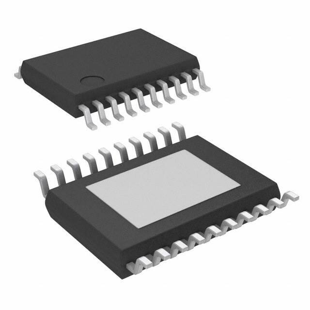
LM5117
HTSSOP (20) PWP
6.50 mm × 4.40 mm
LM5117-Q1
WQFN (24) RTW
4.00 mm × 4.00 mm
(1) For all available packages, see the orderable addendum at
the end of the datasheet.
Typical Application
VIN
SW
UVLO
VIN
DEMB
VCC
HB
RAMP
LM5117
VOUT
HO
VOUT
VCCDIS
SW
COMP
FB
CS
CM
RT
LO
CSG
RES
SS AGND PGND
1
An IMPORTANT NOTICE at the end of this data sheet addresses availability, warranty, changes, use in safety-critical applications,
intellectual property matters and other important disclaimers. PRODUCTION DATA.
�LM5117, LM5117-Q1
SNVS698F – APRIL 2011 – REVISED AUGUST 2015
www.ti.com
Table of Contents
1
2
3
4
5
6
7
Features ..................................................................
Applications ...........................................................
Description .............................................................
Revision History.....................................................
Pin Configuration and Functions .........................
Specifications.........................................................
1
1
1
2
3
5
6.1
6.2
6.3
6.4
6.5
6.6
6.7
6.8
5
5
5
6
6
7
8
9
Absolute Maximum Ratings .....................................
ESD Ratings (LM5117) .............................................
ESD Ratings (LM5117-Q1) .......................................
Recommended Operating Conditions.......................
Thermal Information ..................................................
Electrical Characteristics...........................................
Switching Characteristics ..........................................
Typical Characteristics ..............................................
Detailed Description ............................................ 11
7.1 Overview ................................................................. 11
7.2 Functional Block Diagram ....................................... 12
7.3 Feature Description................................................. 13
7.4 Device Functional Modes........................................ 21
8
Application and Implementation ........................ 22
8.1
8.2
8.3
8.4
Application Information............................................
Typical Applications ...............................................
Detailed Design Procedure .....................................
Application Curves ..................................................
22
22
22
32
9 Power Supply Recommendations...................... 35
10 Layout................................................................... 35
10.1 Layout Guideline ................................................... 35
11 Device and Documentation Support ................. 36
11.1
11.2
11.3
11.4
11.5
Related Links ........................................................
Community Resources..........................................
Trademarks ...........................................................
Electrostatic Discharge Caution ............................
Glossary ................................................................
36
36
36
36
36
12 Mechanical, Packaging, and Orderable
Information ........................................................... 36
4 Revision History
NOTE: Page numbers for previous revisions may differ from page numbers in the current version.
Changes from Revision E (March 2013) to Revision F
Page
•
Added Device Information and Pin Configuration and Functions sections, ESD Rating table, Feature Description,
Device Functional Modes, Application and Implementation, Power Supply Recommendations, Layout, Device and
Documentation Support , and Mechanical, Packaging, and Orderable Information sections ................................................ 1
•
Changed µH into µF ............................................................................................................................................................ 29
Changes from Revision D (March 2013) to Revision E
•
2
Page
Changed layout of National Data Sheet to TI format ........................................................................................................... 34
Submit Documentation Feedback
Copyright © 2011–2015, Texas Instruments Incorporated
Product Folder Links: LM5117 LM5117-Q1
�LM5117, LM5117-Q1
www.ti.com
SNVS698F – APRIL 2011 – REVISED AUGUST 2015
5 Pin Configuration and Functions
PWP Package
20-Pin HTSSOP
Top View
UVLO
1
20
VIN
DEMB
2
19
HB
RES
3
18
HO
SS
4
17
SW
RT
5
16
VCC
15
LO
EP
AGND
6
VCCDIS
7
14
PGND
FB
8
13
CSG
COMP
9
12
CS
CM
10
11
RAMP
UVLO
NC
VIN
NC
HB
HO
RTW Package
24-Pin WQFN
Top View
24
23
22
21
20
19
DEMB
1
18
SW
RES
2
17
NC
SS
3
16
VCC
EP
14
PGND
NC
6
13
CSG
7
8
9
10
11
12
CS
5
RAMP
AGND
CM
LO
COMP
15
FB
4
VCCDIS
RT
Copyright © 2011–2015, Texas Instruments Incorporated
Product Folder Links: LM5117 LM5117-Q1
Submit Documentation Feedback
3
�LM5117, LM5117-Q1
SNVS698F – APRIL 2011 – REVISED AUGUST 2015
www.ti.com
Pin Functions
PIN
HTSSOP
WQFN
NAME
1
24
UVLO
2
3
4
5
4
2
3
4
DESCRIPTION
I
Undervoltage lockout programming pin. If the UVLO pin voltage is below 0.4 V, the
regulator is in the shutdown mode with all functions disabled. If the UVLO pin voltage is
greater than 0.4 V and less than 1.25 V, the regulator is in standby mode with the VCC
regulator operational, the SS pin grounded, and no switching at the HO and LO outputs.
If the UVLO pin voltage is above 1.25 V, the SS pin is allowed to ramp and pulse width
modulated gate drive signals are delivered to the HO and LO pins. A 20μA current
source is enabled when UVLO exceeds 1.25 V and flows through the external UVLO
resistors to provide hysteresis.
I
Optional logic input that enables diode emulation when in the low state. In diode
emulation mode, the low-side NMOS is latched off for the remainder of the PWM cycle
after detecting reverse current flow (current flow from output to ground through the lowside NMOS). When DEMB is high, diode emulation is disabled allowing current to flow in
either direction through the low-side NMOS. A 50-kΩ pull-down resistor internal to the
LM5117 holds DEMB pin low and enables diode emulation if the pin is left floating.
O
The restart timer pin that configures the hiccup mode current limiting. A capacitor on the
RES pin determines the time the controller remains off before automatically restarting.
The hiccup mode commences when the controller experiences 256 consecutive PWM
cycles of cycle-by-cycle current limiting. After this occurs, a 10-μA current source
charges the RES pin capacitor to the 1.25 V threshold and restarts LM5117.
I
An external capacitor and an internal 10-μA current source set the ramp rate of the error
amplifier reference during soft-start. The SS pin is held low when VCC< 5 V, UVLO <
1.25 V or during thermal shutdown.
I
The internal oscillator is programmed with a single resistor between RT and the AGND.
The recommended maximum oscillator frequency is 750kHz. The internal oscillator can
be synchronized to an external clock by coupling a positive pulse into the RT pin through
a small coupling capacitor.
G
Analog ground. Return for the internal 0.8 V voltage reference and analog circuits.
I
Optional input that disables the internal VCC regulator. If VCCDIS>1.25 V, the internal
VCC regulator is disabled. VCCDIS has an internal 500-kΩ pulldown resistor to enable
the VCC regulator when the pin is left floating. The internal 500-kΩ pull-down resistor can
be overridden by pulling VCCDIS above 1.25 V with a resistor divider connected to an
external bias supply.
I
Feedback. Inverting input of the internal error amplifier. A resistor divider from the output
to this pin sets the output voltage level. The regulation threshold at the FB pin is 0.8 V.
O
Output of the internal error amplifier. The loop compensation network should be
connected between this pin and the FB pin.
O
Current monitor output. Average of the sensed inductor current is provided. Monitor
directly between CM and AGND. CM should be left floating when the pin is not used.
I
PWM ramp signal. An external resistor and capacitor connected between the SW pin, the
RAMP pin and the AGND pin sets the PWM ramp slope. Proper selection of component
values produces a RAMP signal that emulates the AC component of the inductor with a
slope proportional to input supply voltage.
I
Current sense amplifier input. Connect to the high-side of the current sense resistor.
G
Kelvin ground connection to the current sense resistor. Connect directly to the low-side of
the current sense resistor.
O
Power ground return pin for low-side NMOS gate driver. Connect directly to the low-side
of the current sense resistor.
RES
SS
RT
5
AGND
7
7
VCCDIS
8
8
FB
9
9
COMP
10
10
CM
11
11
RAMP
12
12
CS
13
13
CSG
14
14
PGND
15
15
LO
16
16
VCC
17
18
SW
19
(1)
DEMB
6
18
(1)
1
TYPE
Low-side NMOS gate drive output. Connect to the gate of the low-side synchronous
NMOS transistor through a short, low inductance path.
P/O/I
I/O
Bias supply pin. Locally decouple to PGND using a low ESR/ESL capacitor located as
close to controller as possible.
O
Switching node of the buck regulator. Connect to the bootstrap capacitor, the source
terminal of the high-side NMOS transistor and the drain terminal of the low-side NMOS
through a short, low inductance path.
P
High-side NMOS gate drive output. Connect to the gate of the high-side NMOS transistor
through a short, low inductance path.
HO
I = Input, O = Output, G = Ground, P = Power
Submit Documentation Feedback
Copyright © 2011–2015, Texas Instruments Incorporated
Product Folder Links: LM5117 LM5117-Q1
�LM5117, LM5117-Q1
www.ti.com
SNVS698F – APRIL 2011 – REVISED AUGUST 2015
Pin Functions (continued)
PIN
HTSSOP
WQFN
NAME
19
20
HB
20
22
VIN
EP
EP
EP
TYPE
(1)
DESCRIPTION
P/I
High-side driver supply for the bootstrap gate drive. Connect to the cathode of the
external bootstrap diode and to the bootstrap capacitor. The bootstrap capacitor supplies
current to charge the high-side NMOS gate and should be placed as close to controller
as possible.
P/I
Supply voltage input source for the VCC regulator.
-
Exposed pad of the package. Electrically isolated. Should be soldered to the ground
plane to reduce thermal resistance.
6
NC
-
No electrical contact.
17
NC
-
No electrical contact.
21
NC
-
No electrical contact.
23
NC
-
No electrical contact.
6 Specifications
6.1 Absolute Maximum Ratings
over operating free-air temperature range (unless otherwise noted) (1)
MIN
MAX
UNIT
VIN to AGND
–0.3
75
V
SW to AGND
–3.0
75
V
HB to SW
–0.3
15
V
–0.3
15
V
VCC to AGND
(2)
HO to SW
–0.3
HB + 0.3
V
LO to AGND
–0.3
VCC + 0.3
V
FB, DEMB, RES, VCCDIS, UVLO to AGND
–0.3
15
V
CM, COMP to AGND
(3)
–0.3
7
V
SS, RAMP, RT to AGND
–0.3
7
V
CS, CSG, PGND, to AGND
–0.3
0.3
V
Storage Temperature, Tstg
–55
150
°C
Junction temperature
–40
150
°C
(1)
(2)
(3)
Stresses beyond those listed under Absolute Maximum Ratings may cause permanent damage to the device. These are stress ratings
only, which do not imply functional operation of the device at these or any other conditions beyond those indicated under Recommended
Operating Conditions. Exposure to absolute-maximum-rated conditions for extended periods may affect device reliability.
See Application and Implementation when input supply voltage is less than the VCC voltage.
These pins are output pins. As such they are not specified to have an external voltage applied.
6.2 ESD Ratings (LM5117)
V(ESD)
(1)
(2)
Electrostatic discharge
VALUE
UNIT
Human-body model (HBM), per ANSI/ESDA/JEDEC JS-001 (1)
±2000
V
Charged-device model (CDM), per JEDEC specification JESD22- V
C101 (2)
±750
V
JEDEC document JEP155 states that 500-V HBM allows safe manufacturing with a standard ESD control process.
JEDEC document JEP157 states that 250-V CDM allows safe manufacturing with a standard ESD control process.
6.3 ESD Ratings (LM5117-Q1)
V(ESD)
(1)
Electrostatic discharge
VALUE
UNIT
Human-body model (HBM), per AEC Q100-002 (1)
±2000
V
Charged-device model (CDM), per AEC Q100-011
±750
V
AEC Q100-002 indicates that HBM stressing shall be in accordance with the ANSI/ESDA/JEDEC JS-001 specification.
Copyright © 2011–2015, Texas Instruments Incorporated
Product Folder Links: LM5117 LM5117-Q1
Submit Documentation Feedback
5
�LM5117, LM5117-Q1
SNVS698F – APRIL 2011 – REVISED AUGUST 2015
www.ti.com
6.4 Recommended Operating Conditions
over operating free-air temperature range (unless otherwise noted) (1)
VIN
(2)
MIN
MAX
UNIT
5.5
65
V
VCC
5.5
14
V
HB to SW
5.5
14
V
Junction temperature
-40
125
°C
(1)
(2)
Recommended Operating Conditions are conditions under which operation of the device is intended to be functional, but does not
ensure specific performance limits. For specifications and test conditions see Electrical Characteristics.
Minimum VIN operating voltage is defined with VCC supplied by the internal HV startup regulator and no external load on VCC. When
VCC is supplied by an external source, minimum VIN operating voltage is 4.5 V.
6.5 Thermal Information
LM5117, LM5117-Q1
THERMAL METRIC
(1)
PWP (HTSSOP)
RTW (WQFN)
20 PINS
24 PINS
UNIT
RθJA
Junction-to-ambient thermal resistance
40
40
°C/W
RθJC(top)
Junction-to-case (top) thermal resistance
4
6
°C/W
(1)
6
For more information about traditional and new thermal metrics, see the Semiconductor and IC Package Thermal Metrics application
report, SPRA953.
Submit Documentation Feedback
Copyright © 2011–2015, Texas Instruments Incorporated
Product Folder Links: LM5117 LM5117-Q1
�LM5117, LM5117-Q1
www.ti.com
SNVS698F – APRIL 2011 – REVISED AUGUST 2015
6.6 Electrical Characteristics
Typical limits are for TJ = 25°C only, represent the most likely parametric norm at TJ = 25°C, and are provided for reference
purposes only; minimum and maximum limits apply over the junction temperature range of –40°C to +125°C. Unless
otherwise specified, the following conditions apply: VVIN = 48 V, VVCCDIS = 0 V, RT = 25 kΩ, no load on LO and HO.
PARAMETER
TEST CONDITIONS
MIN
TYP
MAX
UNIT
VSS = 0 V
4.8
6.2
mA
VSS = 0 V, VVCCDIS = 2 V
0.4
0.55
mA
VSS = 0 V, VUVLO = 0 V
16
40
µA
VIN SUPPLY
IBIAS
VIN operating current
ISHUTDOWN
VIN shutdown current
(1)
VCC REGULATOR
VCC(REG)
VCC regulation
No load
6.85
VVIN = 5.5 V, No external load
VCC dropout (VIN to VCC)
VVIN = 6 V, ICC = 20 mA
VCC sourcing current limit
VVCC = 0 V
30
VSS = 0 V, VVCCDIS = 2 V
IVCC
VCC operating current
(1)
VSS = 0 V, VVCCDIS = 2 V, VVCC = 14
V
VCC undervoltage threshold
VCC rising
4.7
VCC undervoltage hysteresis
7.6
8.2
V
0.05
0.14
V
0.4
0.5
V
42
mA
4
5
mA
5.8
7.3
mA
4.9
5.15
V
0.2
V
VCC DISABLE
VCCDIS threshold
VCCDIS rising
1.22
VCCDIS hysteresis
VCCDIS input current
VVCCDIS = 0 V
VCCDIS pulldown resistance
1.25
1.29
V
0.06
V
-20
nA
500
kΩ
UVLO
UVLO threshold
UVLO rising
UVLO hysteresis current
VUVLO = 1.4 V
UVLO shutdown threshold
UVLO falling
1.22
1.25
1.29
V
15
20
25
µA
0.23
0.3
V
0.1
V
UVLO shutdown hysteresis
SOFT START
ISS
SS current source
VSS = 0 V
7
SS pulldown resistance
10
12
µA
13
24
Ω
800
812
mV
ERROR AMPLIFIER
VREF
FB reference voltage
Measured at FB, FB = COMP
FB input bias current
VFB = 0.8 V
VOH
COMP output high voltage
ISOURCE = 3 mA
VOL
COMP output low voltage
ISINK = 3 mA
AOL
DC gain
ƒBW
Unity gain bandwidth
788
1
nA
2.8
V
0.26
V
80
dB
3
MHz
PWM COMPARATOR
tHO(OFF)
Forced HO Off-time
tON(MIN)
Minimum HO On-time
260
VVIN = 65 V
COMP to PWM comparator offset
320
440
ns
100
ns
1.2
V
OSCILLATOR
ƒSW1
Frequency 1
RT = 25 kΩ
180
200
220
kHz
ƒSW2
Frequency 2
RT = 10 kΩ
430
480
530
kHz
RT output voltage
(1)
1.25
RT sync positive threshold
2.6
Sync pulse width
100
3.2
V
3.95
V
ns
Operating current does not include the current into the RT resistor.
Copyright © 2011–2015, Texas Instruments Incorporated
Product Folder Links: LM5117 LM5117-Q1
Submit Documentation Feedback
7
�LM5117, LM5117-Q1
SNVS698F – APRIL 2011 – REVISED AUGUST 2015
www.ti.com
Electrical Characteristics (continued)
Typical limits are for TJ = 25°C only, represent the most likely parametric norm at TJ = 25°C, and are provided for reference
purposes only; minimum and maximum limits apply over the junction temperature range of –40°C to +125°C. Unless
otherwise specified, the following conditions apply: VVIN = 48 V, VVCCDIS = 0 V, RT = 25 kΩ, no load on LO and HO.
PARAMETER
TEST CONDITIONS
MIN
TYP
MAX
UNIT
106
120
135
mV
CURRENT LIMIT
VCS(TH)
Cycle-by-cycle sense voltage
threshold
VRAMP = 0 V, CSG to CS
CS input bias current
VCS = 0 V
–100
-66
µA
CSG input bias current
VCSG = 0 V
–100
-66
µA
Current sense amplifier gain
Hiccup mode fault timer
10
V/V
256
Cycles
10
µA
RES
IRES
RES Current Source
VRES
RES Threshold
RES Rising
1.22
1.25
1.285
V
2
1.65
V
DIODE EMULATION
VIL
DEMB input low threshold
VIH
DEMB input high threshold
2.5
V
SW zero cross threshold
2.95
–5
mV
DEMB input pulldown resistance
50
kΩ
CURRENT MONITOR
Current monitor amplifier gain
CS to CM
Current monitor amplifier gain
Drift over Temperature
17.5
20.5
23.5
–2
0
2
25
120
mV
Zero input offset
V/V
%
HO GATE DRIVER
VOHH
HO High-state voltage drop
IHO = –100 mA, VOHH = VHB – VHO
0.17
0.3
V
VOLH
HO Low-state voltage drop
IHO = 100 mA, VOLH = VHO – VSW
0.1
0.2
V
(2)
HO rise time
C-load = 1000 pF
HO fall time
C-load = 1000pF (2)
IOHH
Peak HO source current
VHO = 0 V, SW = 0 V, HB = 7.6 V
IOLH
Peak HO sink current
VHO = VHB = 7.6 V
ns
5
ns
2.2
A
3.3
HB to SW undervoltage
HB DC bias current
6
2.56
HB – SW = 7.6 V
A
2.9
3.32
V
65
100
µA
0.17
0.27
V
0.1
0.2
LO GATE DRIVER
VOHL
LO High-state Voltage Drop
ILO = –100 mA, VOHL = VCC-VLO
VOLL
LO Low-state Voltage Drop
ILO = 100 mA, VOLL = VLO
LO rise time
C-load = 1000 pF (2)
LO fall time
C-load = 1000 pF (2)
IOHL
Peak LO source current
VLO = 0 V
IOLL
Peak LO sink current
VLO = 7.6 V
3.3
A
Thermal shutdown
Temperature rising
165
°C
25
°C
V
6
ns
5
ns
2.5
A
THERMAL
TSD
Thermal shutdown hysteresis
(2)
High and low reference are 80% and 20% of the pulse amplitude, respectively.
6.7 Switching Characteristics
over operating free-air temperature range (unless otherwise noted)
PARAMETER
TDLH
LO fall to HO rise delay
TDHL
HO fall to LO rise delay
8
Submit Documentation Feedback
TEST CONDITIONS
MIN
No load
TYP
MAX
UNIT
72
ns
71
ns
Copyright © 2011–2015, Texas Instruments Incorporated
Product Folder Links: LM5117 LM5117-Q1
�LM5117, LM5117-Q1
www.ti.com
SNVS698F – APRIL 2011 – REVISED AUGUST 2015
6.8 Typical Characteristics
Figure 1. HO Peak Driver Current vs Output Voltage
Figure 2. LO Peak Driver Current vs Output Voltage
Figure 3. Driver Dead Time vs VVCC
Figure 4. Driver Dead Time vs Temperature
Figure 5. Forced HO Off-time vs Temperature
Figure 6. Switching Frequency vs RT
Copyright © 2011–2015, Texas Instruments Incorporated
Product Folder Links: LM5117 LM5117-Q1
Submit Documentation Feedback
9
�LM5117, LM5117-Q1
SNVS698F – APRIL 2011 – REVISED AUGUST 2015
www.ti.com
Typical Characteristics (continued)
Figure 7. VVCC vs IVCC
Figure 8. VVCC vs VVIN
Figure 9. VCS(TH) vs Temperature
Figure 10. VREF vs Temperature
Figure 12. Error Amp Gain and Phase vs Frequency
Figure 11. VVCC vs Temperature
10
Submit Documentation Feedback
Copyright © 2011–2015, Texas Instruments Incorporated
Product Folder Links: LM5117 LM5117-Q1
�LM5117, LM5117-Q1
www.ti.com
SNVS698F – APRIL 2011 – REVISED AUGUST 2015
Typical Characteristics (continued)
Figure 13. VCM vs IOUT
Figure 14. VCM vs VCSG-CS
7 Detailed Description
7.1 Overview
The LM5117 high voltage switching controller features all of the functions necessary to implement an efficient
high voltage buck regulator that operates over a very wide input voltage range. This easy to use controller
integrates high-side and low-side NMOS drivers. The regulator control method is based upon peak current mode
control utilizing an emulated current ramp. Peak current mode control provides inherent line feed-forward, cycleby-cycle current limiting and ease of loop compensation. The use of an emulated control ramp reduces noise
sensitivity of the PWM circuit, allowing reliable processing of the very small duty cycles necessary in high input
voltage applications.
The switching frequency is user programmable up to 750 kHz. The RT pin allows the switching frequency to be
programmed by a single resistor or synchronized to an external clock. Fault protection features include cycle-bycycle and hiccup mode current limiting, thermal shutdown and remote shutdown capability by pulling down UVLO
pin. The UVLO input enables the regulator when the input voltage reaches a user selected threshold and
provides a very low quiescent shutdown current when pulled low. A unique analog telemetry feature provides
averaged output current information, allowing various applications that need either a current monitor or current
control. The functional block diagram and typical application circuit of the LM5117 are shown in Functional Block
Diagram.
The device is available in a HTSSOP-20 (6.5 mm x 4.4 mm) package, as well as a WQFN-24 (4 mm × 4 mm)
package which features an exposed pad to aid in thermal dissipation.
Copyright © 2011–2015, Texas Instruments Incorporated
Product Folder Links: LM5117 LM5117-Q1
Submit Documentation Feedback
11
�12
Submit Documentation Feedback
SYNC
CSYNC
CSS
Product Folder Links: LM5117 LM5117-Q1
CRES
CHF
RT
RUV1
RUV2
RCOMP CCOMP
CFT
CIN
REF
RES
RES
Current
COMP
FB
SS
RT
+
+
ERR
+ AMP
-
+
+
-
RESTART
TIMER
-
1.2V
+
STANDBY
REF
STANDBY
SS Current
OSCILLATOR /
SYNC DETECTOR
UVLO
Shutdown
Threshold
UVLO
UVLO
Threshold
UVLO Hysteresis
Current
LM5117
+
AGND
CLK
Q
Q
R
S
STANDBY
VCC OFF
HO_ENABLE
+
PGND
HICCUP MODE
FAULT TIMER
256 CYCLES
C/L
Comparator
RES RESET
HICCUP
10uVCS(TH)
+
500 k:
VCCDIS
Threshold
THERMAL
SHUTDOWN
PWM
Comparator
DE_ENABLE
CLK
STANDBY
VCC OFF
RES RESET
STANDBY
VCCDIS
+
50 k:
DE_ENABLE
DIODE
EMULATION
CONTROL
HB
UVLO
-5 mV
CONDITIONER
VCC
CSG
A=2
RAMP
40 k:
CM
CCM
RCM
RCS2
CCS
RCS1
CS
RGH
RGL
CHB
DHB
RS
CVCC
LO
SW
HO
HB
DEMB
VCC
UVLO
VCC
Current Monitor
Amplifier
Current Sense
Amplifier
A=10
LO Driver
+
-
HO Driver
DISABLE
STANDBY
ZCD
Comparator
2.0 / 2.5V
VCC Regulator
CVIN
LEVEL SHIFT/
ADAPTIVE
TIMER
VCC OFF
LO_ENABLE
HO_ENABLE
DE_ENABLE
VCC OFF
VIN
RVIN
+
-
VIN
QL
QH
CSNB
RSNB
CRAMP
RRAMP
COUT1
LO
RFB1
RFB2
COUT2
VOUT
LM5117, LM5117-Q1
SNVS698F – APRIL 2011 – REVISED AUGUST 2015
www.ti.com
7.2 Functional Block Diagram
Copyright © 2011–2015, Texas Instruments Incorporated
�LM5117, LM5117-Q1
www.ti.com
SNVS698F – APRIL 2011 – REVISED AUGUST 2015
7.3 Feature Description
7.3.1 High Voltage Start-up Regulator and VCC Disable
The LM5117 contains an internal high voltage bias regulator that provides the VCC bias supply for the PWM
controller and NMOS gate drivers. The VIN pin can be connected to an input voltage source as high as 65 V.
The output of the VCC regulator is set to 7.6V. When the input voltage is below the VCC set-point level, the VCC
output tracks the VIN with a small dropout voltage. The output of the VCC regulator is current limited at 30mA
minimum.
Upon power-up, the regulator sources current into the capacitor connected to the VCC pin. The recommended
capacitance range for the pin VCC is 0.47 µF to 10 µF. When the VCC pin voltage exceeds the VCC UV
threshold and the UVLO pin is greater than UVLO threshold, the HO and LO drivers are enabled and a soft-start
sequence begins. The HO and LO drivers remain enabled until either the VCC pin voltage falls below VCC UV
threshold, the UVLO pin voltage falls below UVLO threshold, hiccup mode is activated or the die temperature
exceeds the thermal shutdown threshold. Enabling/Disabling the IC by controlling UVLO is recommended in most
of cases.
An output voltage derived bias supply can be applied to the VCC pin to reduce the controller power dissipation at
higher input voltage. The VCCDIS input can be used to disable the internal VCC regulator when external biasing
is supplied. The externally supplied bias should be coupled to the VCC pin through a diode, preferably a
Schottky diode. If the VCCDIS pin voltage exceeds the VCCDIS threshold, the internal VCC regulator is disabled.
VCCDIS has a 500-kΩ internal pull-down resistor to ground for normal operation with no external bias.
The VCC regulator series pass transistor includes a diode between VCC (Anode) and VIN (Cathode) that should
not be forward biased in normal operation. If the voltage of the external bias supply is greater than the VIN pin
voltage, an external blocking diode is required from the input power supply to the VIN pin to prevent the external
bias supply from passing current to the input supply through VCC.
VIN
VIN
LM5117
External
VCC Supply
VCC
Figure 15. VIN Configuration for VVIN < VVCC
For VOUT between 6 V and 14.5 V, the output can be connected directly to VCC through a diode.
VOUT
VCC
LM5117
VCCDIS resistor divider is
required when external VCC
supplying voltage is smaller
than 8.5V
VCCDIS
Figure 16. External VCC Supply for 6 V < VOUT< 14.5 V
For VOUT < 6 V, a bias winding on the output inductor can be added to generate the external VCC supply voltage.
VCC
LM5117
VCCDIS
VOUT
SW
VCCDIS resistor divider is
required when external VCC
supplying voltage is smaller
than 8.5V
Figure 17. External VCC Supply for VOUT < 6 V
Copyright © 2011–2015, Texas Instruments Incorporated
Product Folder Links: LM5117 LM5117-Q1
Submit Documentation Feedback
13
�LM5117, LM5117-Q1
SNVS698F – APRIL 2011 – REVISED AUGUST 2015
www.ti.com
Feature Description (continued)
For 14.5 V IOUT / 2.
In this example, seven 3.3μF ceramic capacitors were used. With ceramic capacitors, the input ripple voltage will
be triangular. The input ripple voltage can be approximated as:
IOUT
'VIN =
4 x fSW x CIN
[V]
(40)
9A
= 0.42 V
'VIN =
4 x 230 kHz x 3.3 PF x 7
(41)
Capacitors connected in parallel should be evaluated for RMS current rating. The current will split between the
input capacitors based on the relative impedance of the capacitors at the switching frequency.
8.3.18 VIN Filter RVIN, CVIN
An R-C filter (RVIN, CVIN) on VIN is optional. The filter helps to prevent faults caused by high frequency switching
noise injection into the VIN pin. A 0.47-μF ceramic capacitor is used for CVIN in the example. RVIN is selected to
be 3.9 Ω.
8.3.19 Soft-Start Capacitor CSS
The capacitor at the SS pin (CSS) determines the soft-start time (tSS), which is the time for the output voltage to
reach the final regulated value. The tSS for a given CSS can be calculated from Equation 8 as follows:
tSS =
0.1 µF x 0.8V
= 8 ms
10 µA
(42)
For this example, a value of 0.1 μF was chosen for a soft-start time of 8 ms.
8.3.20 Restart Capacitor CRES
The capacitor at the RES pin (CRES) determines tRES, which is the time the LM5117 remains off before a restart
attempt is made in hiccup mode current limiting. tRES for a given CRES can be calculated from Equation 13 as
follows:
tRES =
0.47 µF x 1.25V
= 59 ms
10 µA
(43)
For this example, a value of 0.47 μF was chosen for a restart time of 59 ms.
Copyright © 2011–2015, Texas Instruments Incorporated
Product Folder Links: LM5117 LM5117-Q1
Submit Documentation Feedback
29
�LM5117, LM5117-Q1
SNVS698F – APRIL 2011 – REVISED AUGUST 2015
www.ti.com
8.3.21 Output Voltage Divider RFB2 and RFB1
RFB1 and RFB2 set the output voltage level. The ratio of these resistors is calculated as:
RFB2 VOUT
-1
=
RFB1 0.8V
(44)
The ratio between RCOMP and RFB2 determines the mid-band gain, AFB_MID. A larger value for RFB2 may require a
corresponding larger value for RCOMP. RFB2 should be large enough to keep the total divider power dissipation
small. 4.99 kΩ was chosen for RFB2 in this example, which results in a RFB1 value of 357 Ω for 12-V output.
8.3.22 Loop Compensation Components CCOMP, RCOMP and CHF
RCOMP, CCOMP and CHF configure the error amplifier gain and phase characteristics to produce a stable voltage
loop. For a quick start, follow the 4 steps listed below.
STEP1: Select fCROSS
By selecting one tenth of the switching frequency, fCROSS is calculated as follows:
fCROSS =
fSW
= 23 kHz
10
(45)
STEP2: Determine required RCOMP
Knowing fCROSS, RCOMP is calculated as follows:
RCOMP = 2S x RS x AS x COUT x RFB2 x fCROSS
[:@
(46)
RCOMP = 2S x 7.41 m: x 10 x 514 µF x 4.99 k: x 23 kHz = 27.5 k:
(47)
The standard value of 27.4kΩ was selected for RCOMP
STEP3: Determine CCOMP to cancel load pole
Knowing RCOMP, CCOMP is calculated as follows:
æ 12 V ö
ç
÷ ´ 514 mF
´ COUT è 9 A ø
R
=
= 25nF
CCOMP = LOAD
RCOMP
27.4kW
(48)
The standard value of 22nF was selected for CCOMP
STEP4: Determine CHF to cancel ESR zero
Knowing RCOMP and CCOMP, CHF is calculated as follows:
CHF =
RESR x COUT x CCOMP
RCOMP x CCOMP - RESR x COUT
CHF =
[F]
(49)
10 m: x 514 µF x 22 nF
= 189 pF
27.4k: x 22 nF - 10 m: x 514 µF
(50)
Half of the maximum ESR is assumed as a typical ESR. The standard value of 180pF was selected for CHF.
30
Submit Documentation Feedback
Copyright © 2011–2015, Texas Instruments Incorporated
Product Folder Links: LM5117 LM5117-Q1
�LM5117, LM5117-Q1
www.ti.com
SNVS698F – APRIL 2011 – REVISED AUGUST 2015
Table 1. LM5117 Frequency Analysis Formulas
COMPREHENSIVE FORMULA (1)
SIMPLE FORMULA
MODULATOR
TRANSFER
FUNCTION
s
1+
^
ZZ_ESR
VOUT
= AM x
^
VCOMP
(1 + s )
^
VOUT
= AM x
^
VCOMP
(1 +
ZP_LF
Modulator DC
Gain
AM =
RLOAD
R S x AS
ESR Zero
ZZ_ESR =
ESR Pole
ZZ_ESR = R
Not considered
ZP_ESR = R
Dominant Load
Pole
ZP_LF = R
Sampled Gain
Inductor Pole
1
LOAD
ZP_HF =
Not considered
2
K Factor
K=1
-
^
VCOMP
^
V
OUT
AFB =
AFB_MID =
High
Frequency
Pole
(1)
1+
= AFB x
s
ZZ_EA
s x (1+
-
s
ZP_EA )
1
RFB2 x (CCOMP + CHF)
Mid-band Gain
Low
Frequency
Zero
K=
RCOMP
RFB2
=
fSW
0.5
1
1
+
+ RESR1) x (COUT1 + COUT2) LO x (COUT1 + COUT2) x ZP_HF
or
ZP_HF = Q x Zn
fSW
2
^
V
OUT
1+
= AFB x
s
ZZ_EA
s x (1+
s
ZP_EA )
1
RFB2 x (CCOMP + CHF)
RCOMP
RFB2
1
ZZ_EA = RCOMP x CCOMP
ZP_EA
LOAD
LO
RRAMP x CRAMP x RS x AS
AFB_MID =
1
1
x (COUT1 // COUT2 )
= S x fSW or fn =
^
VCOMP
AFB =
1
x COUT1
S(K - 0.5)
ZSW
Zn =
1
RLOAD
ZP_HF x LO
1
Q=
Feedback DC
Gain
K
Not considered
Sub-harmonic
Double Pole
ESR1
ZP_LF = (R
x COUT
Not considered
Quality Factor
FEEDBACK
TRANSFER
FUNCTION
ESR1
s
ZZ_ESR
s
s
s
s2
x
ZP_LF) (1 + ZP_ESR ) x (1 + ZP_HF + Zn2 )
RLOAD
x
R S x AS 1 +
AM =
1
RESR x COUT
1+
ZZ_EA = RCOMP x CCOMP
1
RCOMP x CHF
ZP_EA
=
1
RCOMP x (CHF // CCOMP)
Comprehensive Equation includes an inductor pole and a gain peaking at fSW/2, which caused by sampling effect of the current mode
control. Also it assumes that a ceramic capacitor COUT2 (No ESR) is connected in parallel with COUT1. RESR1 represents ESR of COUT1 .
Copyright © 2011–2015, Texas Instruments Incorporated
Product Folder Links: LM5117 LM5117-Q1
Submit Documentation Feedback
31
�LM5117, LM5117-Q1
SNVS698F – APRIL 2011 – REVISED AUGUST 2015
www.ti.com
Table 1. LM5117 Frequency Analysis Formulas (continued)
COMPREHENSIVE FORMULA (1)
SIMPLE FORMULA
OPEN-LOOP
RESPONSE
1+
T(s) = AM x AFB x
s
s
1+
ZZ_ESR
ZZ_EA
x
s
)
(1 + Z s ) s x (1 + ZP_EA
P_LF
T(s) =
AM x AFB
s
when ZZ_EA = ZP_LF & ZP_EA = ZZ_ESR
fCROSS =
RCOMP
2 x ' x RS x RFB2 x AS x COUT
when ZZ_EA = ZP_LF & ZP_EA = ZZ_ESR
fCROSS_MAX =
fSW
5
s
1+
ZZ_ESR
ZZ_EA
x
2
s
s
s
s
x (1 +
x (1 +
)
)
)
+ s 2 ) s x (1 + Z
ZP_LF
ZP_ESR
ZP_HF Zn
P_EA
1+
s
ZZ_ESR
2
s
s
(1 + Z ) x (1 + Z
) x (1 + Z s + s 2 )
P_EA
P_ESR
P_HF
Zn
ZZ_EA = ZP_LF
fCROSS =
when
&
Maximum
Cross Over
Frequency
(1 +
AM x AFB
x
T(s) =
s
when
Cross Over
Frequency
(Open Loop
Bandwidth)
s
1+
T(s) = AM x AFB x
RCOMP
2 x ' x RS x RFB2 x AS x (COUT1 + COUT2)
ZZ_EA = ZP_LF
ZP_HF
fCROSS <
2 x S x 10
fCROSS_MAX =
ZP_EA = ZZ_ESR
&
fCROSS <
&
ZP_ESR
2 x S x 10
fSW
x ( 1 + 4 x Q2 -1)
4xQ
The frequency at which 45° phase shift occurs in modulator phase
characteristics.
8.4 Application Curves
Figure 33. Start-Up with Resistive Load
32
Submit Documentation Feedback
Figure 34. Typical Efficiency vs Load Current
Copyright © 2011–2015, Texas Instruments Incorporated
Product Folder Links: LM5117 LM5117-Q1
�LM5117, LM5117-Q1
www.ti.com
SNVS698F – APRIL 2011 – REVISED AUGUST 2015
Application Curves (continued)
8.4.1 Constant Current Regulator
The LM5117 can be configured as a constant current regulator by using the current monitor feature (CM) as the
feedback input. A voltage divider at the VCCDIS pin from VOUT to AGND can be used to protect against output
over-voltage. When the VCCDIS pin voltage is greater than the VCCDIS threshold, the controller disables the
VCC regulator and the VCC pin voltage decays. When the VCC pin voltage is less than the VCC UV threshold,
both HO and LO outputs stop switching. Due to the time delay required for VCC to decay below the VCC UV
threshold, the over-voltage protection operates in hiccup mode. See Figure 35.
VIN
100k:
CIN
UVLO VIN
SW
RES DEMB VCC
15 k:
LM5117
Hiccup Mode OVP 100 k:
Triggered at 13.4V
HB
RAMP
VOUT
CVCC
DHB
CHB
1500 pF
HO
3.24 k:
QH
68 µH
CC Mode: 2A
SW
VCCDIS
LO
332:
VOUT
QL
80 µF
CS
47 m:
0.022 µF
3.24 k:
CSG
CM
COMP
FB
RT
SS
AGND PGND
2.37 k:
22.1 k:
0.47 µF
Current Control (CC)
Figure 35. Constant Current Regulator With Hiccup Mode Output OVP
8.4.2 Constant Voltage and Constant Current Regulator
The LM5117 also can be configured as a constant voltage and constant current regulator, known as CV+CC
regulator. In this configuration, there is much less variation in the current limiting as compared to peak cycle-bycycle current limiting of the inductor current. The LMV431 and the PNP transistor create a voltage-to-current
amplifier in the current loop. This amplifier circuitry does not affect the normal operation when the output current
is less than the current limit set-point. When the output current is greater than the set-point, the PNP transistor
sources a current into CRAMP and increases the positive slope of emulated inductor current ramp until the output
current is less than or equal to the current limit set-point. See Figure 36 and Figure 37.
Copyright © 2011–2015, Texas Instruments Incorporated
Product Folder Links: LM5117 LM5117-Q1
Submit Documentation Feedback
33
�LM5117, LM5117-Q1
SNVS698F – APRIL 2011 – REVISED AUGUST 2015
www.ti.com
Application Curves (continued)
VIN
Current Control (CC)
100 k:
VCC
SW
10 k:
100:
CIN
UVLO VIN
15 k:
RES DEMB VCC
LM5117
100 k:
PNP
CVCC
DHB
HB
RAMP
CHB
1 nF
1500 pF
QH
HO
100 k:
CM
68 PH
VOUT
CV Mode : 5V
CC Mode: 2A
SW
LMV431
200 k:
QL
LO
VCCDIS
80 PF
CS
47 m:
VOUT
3.24 k:
CSG
34.8 k:
0.1 PF
COMP
FB
RT
SS
AGND PGND
619:
22.1 k:
0.33 PF x2
Voltage Control (CV)
Figure 36. Constant Voltage Regulator with Accurate Current Limit
Figure 37. Current Limit Comparison
34
Submit Documentation Feedback
Copyright © 2011–2015, Texas Instruments Incorporated
Product Folder Links: LM5117 LM5117-Q1
�LM5117, LM5117-Q1
www.ti.com
SNVS698F – APRIL 2011 – REVISED AUGUST 2015
9 Power Supply Recommendations
The LM5117 is a power management device. The power supply for the device is any DC voltage source within
the specified input range.
10 Layout
10.1 Layout Guideline
Controller
QL
Place controller as
close to the switches
Inductor
QH
RSENSE
VIN
CIN
COUT
CIN
COUT
GND GND
VOUT
Figure 38. Layout Example
10.1.1 PC Board Layout Recommendation
In a buck regulator the primary switching loop consists of the input capacitor, NMOS power switches and current
sense resistor. Minimizing the area of this loop reduces the stray inductance and minimizes noise and possible
erratic operation. High quality input capacitors should be placed as close as possible to the NMOS power
switches, with the VIN side of the capacitor connected directly to the high-side NMOS drain and the ground side
of the capacitor connected as close as possible to the current sense resistor ground connection.
Connect all of the low power ground connections (RUV1, RT, RFB1, CSS, CRES, CCM, CVIN, CRAMP) directly to the
regulator AGND pin. Connect CVCC directly to the regulator PGND pin. Note that CVIN and CVCC must be as
physically close as possible to the IC. AGND and PGND must be directly connected together through a top-side
copper pattern connected to the exposed pad. Ensure no high current flows beneath the underside exposed pad.
The LM5117 has an exposed thermal pad to aid power dissipation. Adding several vias under the exposed pad
helps conduct heat away from the IC. The junction to ambient thermal resistance varies with application. The
most significant variables are the area of copper in the PC board, the number of vias under the exposed pad and
the amount of forced air cooling. The integrity of the solder connection from the IC exposed pad to the PC board
is critical. Excessive voids greatly decrease the thermal dissipation capacity.
The highest power dissipating components are the two power switches. Selecting NMOS switches with exposed
pads aids the power dissipation of these devices.
Copyright © 2011–2015, Texas Instruments Incorporated
Product Folder Links: LM5117 LM5117-Q1
Submit Documentation Feedback
35
�LM5117, LM5117-Q1
SNVS698F – APRIL 2011 – REVISED AUGUST 2015
www.ti.com
11 Device and Documentation Support
11.1 Related Links
The table below lists quick access links. Categories include technical documents, support and community
resources, tools and software, and quick access to sample or buy.
Table 2. Related Links
PARTS
PRODUCT FOLDER
SAMPLE & BUY
TECHNICAL
DOCUMENTS
TOOLS &
SOFTWARE
SUPPORT &
COMMUNITY
LM5117
Click here
Click here
Click here
Click here
Click here
LM5117-Q1
Click here
Click here
Click here
Click here
Click here
11.2 Community Resources
The following links connect to TI community resources. Linked contents are provided "AS IS" by the respective
contributors. They do not constitute TI specifications and do not necessarily reflect TI's views; see TI's Terms of
Use.
TI E2E™ Online Community TI's Engineer-to-Engineer (E2E) Community. Created to foster collaboration
among engineers. At e2e.ti.com, you can ask questions, share knowledge, explore ideas and help
solve problems with fellow engineers.
Design Support TI's Design Support Quickly find helpful E2E forums along with design support tools and
contact information for technical support.
11.3 Trademarks
E2E is a trademark of Texas Instruments.
WEBENCH is a registered trademark of Texas Instruments.
All other trademarks are the property of their respective owners.
11.4 Electrostatic Discharge Caution
These devices have limited built-in ESD protection. The leads should be shorted together or the device placed in conductive foam
during storage or handling to prevent electrostatic damage to the MOS gates.
11.5 Glossary
SLYZ022 — TI Glossary.
This glossary lists and explains terms, acronyms, and definitions.
12 Mechanical, Packaging, and Orderable Information
The following pages include mechanical, packaging, and orderable information. This information is the most
current data available for the designated devices. This data is subject to change without notice and revision of
this document. For browser-based versions of this data sheet, refer to the left-hand navigation.
36
Submit Documentation Feedback
Copyright © 2011–2015, Texas Instruments Incorporated
Product Folder Links: LM5117 LM5117-Q1
�PACKAGE OPTION ADDENDUM
www.ti.com
10-Dec-2020
PACKAGING INFORMATION
Orderable Device
Status
(1)
Package Type Package Pins Package
Drawing
Qty
Eco Plan
(2)
Lead finish/
Ball material
MSL Peak Temp
Op Temp (°C)
Device Marking
(3)
(4/5)
(6)
LM5117PMH/NOPB
ACTIVE
HTSSOP
PWP
20
73
RoHS & Green
SN
Level-3-260C-168 HR
-40 to 125
LM5117
PMH
LM5117PMHE/NOPB
ACTIVE
HTSSOP
PWP
20
250
RoHS & Green
SN
Level-3-260C-168 HR
-40 to 125
LM5117
PMH
LM5117PMHX/NOPB
ACTIVE
HTSSOP
PWP
20
2500
RoHS & Green
SN
Level-3-260C-168 HR
-40 to 125
LM5117
PMH
LM5117PSQ/NOPB
ACTIVE
WQFN
RTW
24
1000
RoHS & Green
SN
Level-1-260C-UNLIM
-40 to 125
L5117P
LM5117PSQE/NOPB
ACTIVE
WQFN
RTW
24
250
RoHS & Green
SN
Level-1-260C-UNLIM
-40 to 125
L5117P
LM5117PSQX/NOPB
ACTIVE
WQFN
RTW
24
4500
RoHS & Green
SN
Level-1-260C-UNLIM
-40 to 125
L5117P
LM5117QPMH/NOPB
ACTIVE
HTSSOP
PWP
20
73
RoHS & Green
SN
Level-3-260C-168 HR
-40 to 125
LM5117
QMH
LM5117QPMHE/NOPB
ACTIVE
HTSSOP
PWP
20
250
RoHS & Green
SN
Level-3-260C-168 HR
-40 to 125
LM5117
QMH
LM5117QPMHX/NOPB
ACTIVE
HTSSOP
PWP
20
2500
RoHS & Green
SN
Level-3-260C-168 HR
-40 to 125
LM5117
QMH
LM5117QPSQ/NOPB
ACTIVE
WQFN
RTW
24
1000
RoHS & Green
SN
Level-1-260C-UNLIM
-40 to 125
L5117Q
LM5117QPSQE/NOPB
ACTIVE
WQFN
RTW
24
250
RoHS & Green
SN
Level-1-260C-UNLIM
-40 to 125
L5117Q
LM5117QPSQX/NOPB
ACTIVE
WQFN
RTW
24
4500
RoHS & Green
SN
Level-1-260C-UNLIM
-40 to 125
L5117Q
(1)
The marketing status values are defined as follows:
ACTIVE: Product device recommended for new designs.
LIFEBUY: TI has announced that the device will be discontinued, and a lifetime-buy period is in effect.
NRND: Not recommended for new designs. Device is in production to support existing customers, but TI does not recommend using this part in a new design.
PREVIEW: Device has been announced but is not in production. Samples may or may not be available.
OBSOLETE: TI has discontinued the production of the device.
(2)
RoHS: TI defines "RoHS" to mean semiconductor products that are compliant with the current EU RoHS requirements for all 10 RoHS substances, including the requirement that RoHS substance
do not exceed 0.1% by weight in homogeneous materials. Where designed to be soldered at high temperatures, "RoHS" products are suitable for use in specified lead-free processes. TI may
reference these types of products as "Pb-Free".
RoHS Exempt: TI defines "RoHS Exempt" to mean products that contain lead but are compliant with EU RoHS pursuant to a specific EU RoHS exemption.
Addendum-Page 1
Samples
�PACKAGE OPTION ADDENDUM
www.ti.com
10-Dec-2020
Green: TI defines "Green" to mean the content of Chlorine (Cl) and Bromine (Br) based flame retardants meet JS709B low halogen requirements of


 工商网监
湘ICP备2023018690号
工商网监
湘ICP备2023018690号
