LM5143-Q1
SNVSB29C – OCTOBER 2018 – REVISED JUNE 2021
LM5143-Q1 Automotive 3.5-V to 65-V Dual Synchronous Buck Controller With Low IQ
1 Features
2 Applications
•
•
•
•
•
•
•
•
•
•
•
•
AEC-Q100 qualified for automotive applications:
– Device temperature grade 1: –40°C to +125°C
ambient operating temperature
Functional Safety-Capable
– Documentation available to aid functional safety
system design
Versatile synchronous buck DC/DC controller
– Wide input voltage range of 3.5 V to 65 V
– 1% accurate, fixed 3.3-V, 5-V, or adjustable
outputs from 0.6 V to 55 V
– 150°C maximum junction temperature
– Shutdown mode current: 4 µA typical
– No-load standby current: 15 µA typical
Two interleaved synchronous buck channels
– Dual-channel or single-output multiphase
– 65-ns tON(min) for high VIN/VOUT ratio
– 60-ns tOFF(min) for low dropout
Inherent protection features for robust design
– Hiccup-mode overcurrent protection
– Independent ENABLE and PGOOD functions
– VCC, VDDA, and gate-drive UVLO protection
– Thermal shutdown protection with hysteresis
Optimized for ultra-low EMI requirements
– Slew-rate controlled adaptive gate drivers
– Spread spectrum reduces peak emissions
– Optimized for CISPR 25 Class 5 requirements
Switching frequency from 100 kHz to 2.2 MHz
– SYNC in and SYNC out capability
– Selectable diode emulation or FPWM
VQFNP-40 pacakge with wettable flank pins
Create a custom design using the LM5143-Q1 with
WEBENCH® Power Designer
Automotive electronic systems
Infotainment systems, instrument clusters
Advanced driver assistance systems (ADAS)
3 Description
The LM5143-Q1 is a 65-V synchronous buck DC/DC
controller for high-current single or dual outputs.
The device uses an interleaved, stackable, peak
current-mode control architecture for easy loop
compensation, fast transient response, excellent load
and line regulation, and accurate current sharing with
paralleled phases for higher output current. A highside switch minimum on-time of 65 ns gives large
step-down ratios, enabling the direct conversion from
12-V, 24-V, or 48-V automotive inputs to low-voltage
rails for reduced system complexity and solution cost.
The LM5143-Q1 continues to operate during input
voltage dips as low as 3.5 V, at nearly 100% duty
cycle if needed.
Current is sensed using the inductor DCR for highest
efficiency or an optional shunt resistor for high
accuracy. The 15-μA no-load quiescent current with
the output voltage in regulation extends operating
run-time in battery-powered systems. Power the
LM5143-Q1 from the output of the switching regulator
or another available source for even lower input
quiescent current and power loss.
Device Information
PACKAGE(1)
PART NUMBER
LM5143-Q1
(1)
VQFNP (40)
BODY SIZE (NOM)
6.00 mm × 6.00 mm
For all available packages, see the orderable addendum at
the end of the data sheet.
VIN = 3.5 V...65 V
VDDA
CIN
HB1
VOUT1 = 3.3 V
IOUT1 = 10 A R
CO1
VCC
VIN FB1 FB2 MODE
HB2
QH1
S1
QH2
LO1
HO1
HO2
HOL1
HOL2
SW1
SW2
LO1
LOL1
LO2
LOL2
QL1
PGND1
VIN
LM5143-Q1
RS2
VOUT2 = 5 V
IOUT2 = 10 A
CO2
QL2
PGND2
EN1
EN2
RT
PG2
PG1
LO2
VIN
SYNCOUT
CS1
VOUT1
DEMB
CS2
VOUT2
COMP1
COMP2
VCCX
AGND SS1 RES SS2 VDDA DITH
* VOUT1 tracks VIN if VIN < 3.7 V
VOUT2 tracks VIN if VIN < 5.4 V
High-Efficiency Dual Step-Down Regulator
An IMPORTANT NOTICE at the end of this data sheet addresses availability, warranty, changes, use in safety-critical applications,
intellectual property matters and other important disclaimers. PRODUCTION DATA.
�LM5143-Q1
www.ti.com
SNVSB29C – OCTOBER 2018 – REVISED JUNE 2021
Table of Contents
1 Features............................................................................1
2 Applications..................................................................... 1
3 Description.......................................................................1
4 Revision History.............................................................. 2
5 Description (continued).................................................. 3
6 Pin Configuration and Functions...................................4
6.1 Wettable Flanks.......................................................... 6
7 Specifications.................................................................. 7
7.1 Absolute Maximum Ratings ....................................... 7
7.2 ESD Ratings .............................................................. 7
7.3 Recommended Operating Conditions ........................8
7.4 Thermal Information ...................................................8
7.5 Electrical Characteristics ............................................8
7.6 Switching Characteristics .........................................12
7.7 Typical Characteristics.............................................. 13
8 Detailed Description......................................................18
8.1 Overview................................................................... 18
8.2 Functional Block Diagram......................................... 19
8.3 Feature Description...................................................20
8.4 Device Functional Modes..........................................32
9 Application and Implementation.................................. 33
9.1 Application Information............................................. 33
9.2 Typical Applications.................................................. 41
10 Power Supply Recommendations..............................52
11 Layout........................................................................... 53
11.1 Layout Guidelines................................................... 53
11.2 Layout Example...................................................... 56
12 Device and Documentation Support..........................58
12.1 Device Support....................................................... 58
12.2 Documentation Support.......................................... 59
12.3 Receiving Notification of Documentation Updates..59
12.4 Support Resources................................................. 59
12.5 Trademarks............................................................. 60
12.6 Electrostatic Discharge Caution..............................60
12.7 Glossary..................................................................60
13 Mechanical, Packaging, and Orderable
Information.................................................................... 60
4 Revision History
NOTE: Page numbers for previous revisions may differ from page numbers in the current version.
Changes from Revision B (October 2019) to Revision C (June 2021)
Page
• Updated Section 1 to include functional safety bullet......................................................................................... 1
• Removed "DC/DC" from data sheet title.............................................................................................................1
• Updated the numbering format for tables, figures and cross-references throughout the document...................1
• Added the Mode pin to the Absolute Maximum Ratings and Recommended Operating Conditions .................7
• Changed resistor value from 100 k to 220 k for tSYNCOUT1 and tSYNCOUT2 ........................................................ 8
• Added note in Section 9.2.1.2.7 .......................................................................................................................45
• Updated Section 11.2 .......................................................................................................................................56
• Added Table 12-1 in Section 12 .......................................................................................................................58
Changes from Revision A (May 2019) to Revision B (October 2019)
Page
• Changed device status from Advance Information to Production Data ............................................................. 1
2
Submit Document Feedback
Copyright © 2021 Texas Instruments Incorporated
Product Folder Links: LM5143-Q1
�LM5143-Q1
www.ti.com
SNVSB29C – OCTOBER 2018 – REVISED JUNE 2021
5 Description (continued)
Several features are included to simplify compliance with CISPR 25 and automotive EMI requirements.
Adaptively timed, high-current MOSFET gate drivers with adjustable slew rate control minimize body diode
conduction during switching transitions, reducing switching losses and improving thermal and EMI performance
at high input voltage and high switching frequency. To reduce input capacitor ripple current and EMI filter size,
180° interleaved operation is provided for two outputs. A 90° out-of-phase clock output works well for cascaded,
multi-channel, or multi-phase power stages. Resistor-adjustable switching frequency as high as 2.2 MHz can
be synchronized to an external clock source up to 2.5 MHz to eliminate beat frequencies in noise-sensitive
applications. Optional triangular spread spectrum modulation further improves the EMI signature.
Additional features of the LM5143-Q1 include 150°C maximum junction temperature operation, user-selectable
diode emulation for lower current consumption at light-load conditions, configurable soft-start functions, opendrain Power-Good flags for fault reporting and output monitoring, independent enable inputs, monotonic start-up
into prebiased loads, integrated VCC bias supply regulator, programmable hiccup-mode overload protection, and
thermal shutdown protection with automatic recovery.
The LM5143-Q1 controller comes in a 6-mm × 6-mm thermally-enhanced, 40-pin VQFNP package with wettable
flank pins to facilitate optical inspection during manufacturing.
Submit Document Feedback
Copyright © 2021 Texas Instruments Incorporated
Product Folder Links: LM5143-Q1
3
�LM5143-Q1
www.ti.com
SNVSB29C – OCTOBER 2018 – REVISED JUNE 2021
EN2
SYNCOUT
DITH
RT
VDDA
AGND
MODE
DEMB
RES
EN1
40
39
38
37
36
35
34
33
32
31
6 Pin Configuration and Functions
SS2
1
30
SS1
COMP2
2
29
COMP1
FB2
3
28
FB1
CS2
4
27
CS1
VOUT2
5
26
VOUT1
Exposed Pad (EP) on Bottom
Connect to Ground
SW1
HB1
20
21
19
10
LOL1
SW2
18
HO1
LO1
22
17
9
PGND1
HO2
16
HOL1
VCC
23
15
8
VCC
HOL2
14
PG1
PGND2
24
13
7
LO2
PG2
12
VIN
LOL2
25
11
6
HB2
VCCX
Connect Exposed Pad on the bottom to AGND and PGND on the PCB.
Figure 6-1. RWG Package 40-Pin VQFNP with Wettable Flanks (Top View)
4
Submit Document Feedback
Copyright © 2021 Texas Instruments Incorporated
Product Folder Links: LM5143-Q1
�LM5143-Q1
www.ti.com
SNVSB29C – OCTOBER 2018 – REVISED JUNE 2021
Table 6-1. Pin Functions
PIN
NO.
NAME
I/O (1)
DESCRIPTION
1
SS2
I
Channel 2 soft-start programming pin. An external ceramic capacitor and an internal 20-μA current source
set the ramp rate of the internal error amplifier reference during soft start. Pulling SS2 below 150 mV turns
off the channel 2 gate driver outputs, but all the other functions remain active.
2
COMP2
O
Output of the channel 2 transconductance error amplifier. COMP2 is high impedance in interleave or slave
mode.
3
FB2
I
Feedback input of channel 2. Connect FB2 to VDDA for a 3.3-V output or connect FB2 to AGND for a fixed
5-V output. A resistive divider from VOUT2 to FB2 sets the output voltage level between 0.6 V and 55 V.
The regulation threshold at FB2 is 0.6 V.
4
CS2
I
Channel 2 current sense amplifier input. Connect CS2 to the inductor side of the external current sense
resistor (or to the relevant sense capacitor terminal if inductor DCR current sensing is used) using a
low-current Kelvin connection.
5
VOUT2
I
Output voltage sense and the current sense amplifier input of channel 2. Connect VOUT2 to the output side
of the channel 2 current sense resistor (or to the relevant sense capacitor terminal if inductor DCR current
sensing is used).
6
VCCX
P
Optional input for an external bias supply. If VVCCX > 4.3 V, VCCX is internally connected to VCC and the
internal VCC regulator is disabled. Connect a ceramic capacitor between VCCX and PGND.
7
PG2
O
An open-collector output which goes low if VOUT2 is outside a specified regulation window.
8
HOL2
O
Channel 2 high-side gate driver turnoff output.
9
HO2
O
Channel 2 high-side gate driver turnon output.
10
SW2
P
Switching node of the channel 2 buck regulator. Connect to the bootstrap capacitor, the source terminal of
the high-side MOSFET, and the drain terminal of the low-side MOSFET.
11
HB2
P
Channel 2 high-side driver supply for bootstrap gate drive.
12
LOL2
O
Channel 2 low-side gate driver turnoff output.
13
LO2
O
Channel 2 low-side gate driver turnon output.
14
PGND2
G
Power ground connection pin for low-side NMOS gate driver.
VCC
P
VCC bias supply pin. Pins 15 and 16 must to be connected together on the PCB. Connect ceramic
capacitors between VCC and PGND1 and between VCC and PGND2.
17
PGND1
G
Power ground connection pin for low-side NMOS gate driver.
18
LO1
O
Channel 1 low-side gate driver turnon output.
19
LOL1
O
Channel 1 low-side gate driver turnoff output.
20
HB1
P
Channel 1 high-side driver supply for bootstrap gate drive.
21
SW1
P
Switching node of the channel 1 buck regulator. Connect to the channel 1 bootstrap capacitor, the source
terminal of the high-side MOSFET and the drain terminal of the low-side MOSFET.
22
HO1
O
Channel 1 high-side gate driver turnon output.
23
HOL1
O
Channel 1 high-side gate driver turnoff output.
24
PG1
O
An open-collector output that goes low if VOUT1 is outside a specified regulation window.
25
VIN
P
Supply voltage input source for the VCC regulators.
26
VOUT1
I
Output voltage sense and the current sense amplifier input of channel 1. Connect VOUT1 to the output side
of the channel 1 current sense resistor (or to the relevant sense capacitor terminal if inductor DCR current
sensing is used).
27
CS1
I
Channel 1 current sense amplifier input. Connect CS1 to the inductor side of the external current sense
resistor (or to the relevant sense capacitor terminal if inductor DCR current sensing is used) using a
low-current Kelvin connection.
28
FB1
I
Feedback input of channel 1. Connect the FB1 pin to VDDA for a 3.3-V output or connect FB1 to AGND for
a 5-V output. A resistive divider from VOUT1 to FB1 sets the output voltage level between 0.6 V and 55 V.
The regulation threshold at FB1 is 0.6 V.
29
COMP1
O
Output of the channel 1 transconductance error amplifier (EA).
30
SS1
I
Channel 1 soft-start programming pin. An external capacitor and an internal 20-μA current source set the
ramp rate of the internal error amplifier reference during soft start. Pulling the SS1 voltage below 150 mV
turns off the channel 1 gate driver outputs, but the all the other functions remain active.
15, 16
Submit Document Feedback
Copyright © 2021 Texas Instruments Incorporated
Product Folder Links: LM5143-Q1
5
�LM5143-Q1
www.ti.com
SNVSB29C – OCTOBER 2018 – REVISED JUNE 2021
Table 6-1. Pin Functions (continued)
PIN
NO.
31
NAME
EN1
I/O (1)
DESCRIPTION
I
An active high input (VEN1 > 2 V) enables Output 1. If Outputs 1 and 2 are disabled, the LM5143-Q1 is in
shutdown mode unless a SYNC signal is present at DEMB. EN1 must never be floating.
32
RES
O
Restart timer pin. An external capacitor configures the hiccup-mode current limiting. A capacitor at the RES
pin determines the time the controller remains off before automatically restarting in hiccup mode. The two
regulator channels operate independently. One channel can operate in normal mode while the other is
in hiccup-mode overload protection. The hiccup mode commences when either channel experiences 512
consecutive PWM cycles with cycle-by-cycle current limiting. Connect RES to VDDA during power-up to
disable hiccup-mode protection.
33
DEMB
I
Diode Emulation pin. Connect DEMB to AGND to enable diode emulation mode. Connect DEMB to VDDA
to operate the LM5143-Q1 in forced PWM (FPWM) mode with continuous conduction at light loads. DEMB
can also be used as a synchronization input to synchronize the internal oscillator to an external clock.
34
MODE
I
Connect MODE to AGND or VDDA for dual-output or interleaved single-output operation, respectively. This
also configures the LM5143-Q1 with an EA transconductance of 1200 µS. Connecting a 10-kΩ resistor
between MODE and AGND sets the LM5143-Q1 for dual-output operation with an ultra-low IQ mode and an
EA transconductance of 60 µS.
35
AGND
G
Analog ground connection. Ground return for the internal voltage reference and analog circuits.
36
VDDA
O
Internal analog bias regulator output. Connect a ceramic decoupling capacitor from VDDA to AGND.
37
RT
I
Frequency programming pin. A resistor from RT to AGND sets the oscillator frequency between 100 kHz
and 2.2 MHz.
38
DITH
I
A capacitor connected between the DITH pin and AGND is charged and discharged with a 20-µA current
source. If dithering is enabled, the voltage on the DITH pin ramps up and down modulating the oscillator
frequency between –5% and +5% of the internal oscillator. Connecting DITH to VDDA during power-up
disables the dither feature. DITH is ignored if an external synchronization clock is used.
39
SYNCOUT
O
SYNCOUT is a logic level signal with a rising edge approximately 90° lagging HO2 (or 90° leading HO1).
When the SYNCOUT signal is used to synchronize a second LM5143-Q1 controller, all phases are 90° out
of phase.
40
EN2
I
An active high input (VEN2 > 2 V) enables Output 2. If Outputs 1 and 2 are disabled, the LM5143-Q1 is in
shutdown mode unless a SYNC signal is present on DEMB. EN2 must never be floating.
(1)
P = Power, G = Ground, I = Input, O = Output
6.1 Wettable Flanks
100% automated visual inspection (AVI) post-assembly is typically required to meet requirements for high
reliability and robustness. Standard quad-flat no-lead (QFN) packages do not have solderable or exposed pins
and terminals that are easily viewed. It is therefore difficult to visually determine whether or not the package is
successfully soldered onto the printed-circuit board (PCB). The wettable-flank process was developed to resolve
the issue of side-lead wetting of leadless packaging. The LM5143-Q1 is assembled using a 40-pin VQFNP
package with wettable flanks to provide a visual indicator of solderability, which reduces the inspection time and
manufacturing costs.
6
Submit Document Feedback
Copyright © 2021 Texas Instruments Incorporated
Product Folder Links: LM5143-Q1
�LM5143-Q1
www.ti.com
SNVSB29C – OCTOBER 2018 – REVISED JUNE 2021
7 Specifications
7.1 Absolute Maximum Ratings
Over the recommended operating junction temperature range of –40°C to 150°C (unless otherwise noted)(1)
MIN
VIN to PGND
–0.3
70
SW1, SW2 to PGND
–0.3
70
SW1, SW2 to PGND (20-ns transient)
HB1 to SW1, HB2 to SW2
HO1 to SW1, HOL1 to SW1, HO2 to SW2, HOL2 to SW2
HO1 to SW1, HOL1 to SW1, HO2 to SW2, HOL2 to SW2 (20-ns transient)
UNIT
–5
–0.3
HB1 to SW1, HB2 to SW2 (20-ns transient)
Input voltage
MAX
6.5
–5
–0.3
VHB + 0.3
–5
–0.3
LO1, LOL1, LO2, LOL2 to PGND (20-ns transient)
–1.5
VVCC + 0.3
SS1, SS2, COMP1, COMP2, RES, RT, MODE, DITH to AGND
–0.3
VVDDA + 0.3
EN1, EN2 to PGND
–0.3
70
VCC, VCCX, VDDA, PG1, PG2, DEMB, FB1, FB2 to AGND
–0.3
6.5
VOUT1, VOUT2, CS1, CS2
–0.3
60
VOUT1 to CS1, VOUT2 to CS2
–0.3
0.3
PGND to
AGND
–0.3
0.3
V
Operating junction temperature, TJ
–40
150
°C
Storage temperature, Tstg
–40
150
°C
(1)
VVCC + 0.3
V
LO1, LOL1, LO2, LOL2 to PGND
Stresses beyond those listed under Absolute Maximum Ratings may cause permanent damage to the device. These are stress
ratings only, which do not imply functional operation of the device at these or any other conditions beyond those indicated under
Recommended Operating Conditions. Exposure to absolute-maximum-rated conditions for extended periods may affect device
reliability.
7.2 ESD Ratings
VALUE
UNIT
±2000
V
Corner pins
±750
V
Other pins
±500
V
Human body model (HBM), per AEC-Q100-002 (1)
HBM ESD Classification Level 2
V(ESD)
(1)
Electrostatic discharge
Charge device model (CDM), per AEC-Q100-011,
CDM ESD Classification Level C4B
AEC Q100-002 indicates that HBM stressing shall be in accordance with the ANSI/ESDA/JEDEC JS-001 specification
Submit Document Feedback
Copyright © 2021 Texas Instruments Incorporated
Product Folder Links: LM5143-Q1
7
�LM5143-Q1
www.ti.com
SNVSB29C – OCTOBER 2018 – REVISED JUNE 2021
7.3 Recommended Operating Conditions
Over the recommended operating junction temperature range of –40°C to 150°C (unless otherwise noted).
MIN
Input voltage
range
VIN
TJ
VIN to PGND
–0.3
SW1, SW2 to PGND
–0.3
HB1 to SW1, HB2 to SW2
–0.3
HO1 to SW1, HOL1 to SW1, HO2 to SW2, HOL2 to SW2
–0.3
LO1, LOL1, LO2, LOL2 to PGND
–0.3
FB1, FB2, SS1, SS2, COMP1, COMP2, RES, DEMB, RT,
MODE, DITH to AGND
–0.3
EN1, EN2 to PGND
–0.3
VCC, VCCX, VDDA to PGND
–0.3
VOUT1, VOUT2, CS1, CS2 to PGND
NOM
MAX
UNIT
65
65
5
5.25
VHB + 0.3
5
5.25
V
5.25
65
5
5.25
–0.3
55
PGND to AGND
–0.3
0.3
Operating
junction
temperature
–40
150
°C
7.4 Thermal Information
LM5143-Q1
THERMAL METRIC(1)
RWG (VQFNP)
UNIT
40 PINS
RΘJA
Junction-to-ambient thermal resistance
34.8
°C/W
RΘJC(top)
Junction-to-case (top) thermal resistance
22.8
°C/W
RΘJB
Junction-to-board thermal resistance
9.5
°C/W
RΘJC(bot)
Junction-to-case (bottom) thermal resistance
1.3
°C/W
ΨJB
Junction-to-board characterization parameter
9.4
°C/W
ΨJT
Junction-to-top characterization parameter
0.3
°C/W
(1)
For more information about traditional and new thermal metrics, see the Semiconductor and IC Package Thermal Metrics application
report, SPRA953.
7.5 Electrical Characteristics
Over the recommended operating junction temperature range of –40°C to 150°C (unless otherwise noted), Typical values
correspond to TJ = 25℃, VVIN = 12 V, VVCCX = 5 V, VVOUT1 = 3.3 V, VVOUT2 = 5 V, VEN1 = VEN2 = 5 V, RRT = 10 kΩ, FSW = 2.2
MHz, no-load on the drive outputs (HO1, HOL1, LO1, LOL1, HO2, HOL2, LO2 and LOL2).
PARAMETER
TEST CONDITIONS
MIN
TYP
MAX
UNIT
INPUT VOLTAGE (VIN)
ISHUTDOWN
Shutdown mode current
VIN = 12 V, VEN1 = VEN2 = 0 V
3.3
7
µA
ISTANDBY1
Standby current, channel 1
VIN = 12 V, VEN1 = 5 V, VEN2 = 0 V, VVOUT1
= 3.3 V, in regulation, no-load, not switching,
DEMB = MODE = GND
24
31
µA
ISTANDBY2
Standby current, channel 2
VIN = 12 V, VEN1 = 0 V, VEN2 = 5 V, VVOUT2 = 5
V, in regulation, no-load, not switching, DEMB
= MODE = AGND
25
43
µA
ISTANDBY3
VIN = 12 V, VEN1 = 5 V, VEN2 = 0 V, VVOUT1
Standby current, channel 1, ultra-low
= 3.3 V, in regulation, no-load, not switching,
IQ mode
DEMB = GND, RMODE = 10 kΩ to GND
15
21
µA
ISTANDBY4
VIN = 12 V, VEN1 = 0 V, VEN2 = 5 V, VVOUT2 = 5
Standby current, channel 2, ultra-low
V, in regulation, no-load, not switching, DEMB
IQ mode
= GND, RMODE = 10 kΩ to AGND
21
33
µA
BIAS REGULATOR (VCC)
8
Submit Document Feedback
Copyright © 2021 Texas Instruments Incorporated
Product Folder Links: LM5143-Q1
�LM5143-Q1
www.ti.com
SNVSB29C – OCTOBER 2018 – REVISED JUNE 2021
Over the recommended operating junction temperature range of –40°C to 150°C (unless otherwise noted), Typical values
correspond to TJ = 25℃, VVIN = 12 V, VVCCX = 5 V, VVOUT1 = 3.3 V, VVOUT2 = 5 V, VEN1 = VEN2 = 5 V, RRT = 10 kΩ, FSW = 2.2
MHz, no-load on the drive outputs (HO1, HOL1, LO1, LOL1, HO2, HOL2, LO2 and LOL2).
MIN
TYP
MAX
VCC regulation voltage
PARAMETER
VVIN = 12 V, IVCC = 100 mA, VVCCX = 0 V
4.7
5
5.3
VCC-UVLO
VCC UVLO rising threshold
VVCC rising
3.2
3.3
3.4
VVCC-HYST
VCC UVLO hysteresis
IVCC-LIM
VCC sourcing current limit
VVCC-REG
TEST CONDITIONS
UNIT
V
V
175
mV
-250
mA
ANALOG BIAS (VDDA)
VVDDA-REG
VDDA regulation voltage
VVDDA-UVLO
VDDA UVLO rising threshold
VVCC rising, VVCCX = 0 V
4.75
5
5.25
V
3.1
3.2
3.3
V
VVDDA-HYST
VDDA UVLO hysteresis
VVCCX = 0 V
90
mV
RVDDA
VDDA resistance
VVCCX = 0 V
20
Ω
EXTERNAL BIAS (VCCX)
VVCCX-ON
VCCX(ON) rising threshold
RVCCX
VCCX resistance
VVCCX-HYST
VCCX hysteresis voltage
4.1
VVCCX = 5 V
4.3
4.4
V
1.3
Ω
130
mV
CURRENT LIMIT (CS1, CS2)
VCS1
Current limit threshold 1
Measured from CS1 to VOUT1
66
Measured from CS2 to VOUT2
66
VCS2
Current limit threshold 2
TCS-DELAY
CS delay to output
GCS
CS amplifier gain
ICS-BIAS
CS amplifier input bias current
73
80
mV
73
80
mV
40
11.4
12
ns
12.6
V/V
15
nA
POWER GOOD (PG1, PG2)
PG1UV
PG1 UV trip level
Falling with respect to the regulation voltage
90%
92%
PG2UV
PG2 UV trip level
Falling with respect to the regulation voltage
90%
92%
94%
PG1OV
PG1 OV trip level
Rising with respect to the regulation voltage
108%
110%
112%
108%
110%
112%
PG2OV
PG2 OV trip level
Rising with respect to the regulation voltage
PG1UV-HYST
PG1 UV hysteresis
Rising with respect to the regulation voltage
3.4%
PG1OV-HYST
PG1 OV hysteresis
Rising with respect to the regulation voltage
3.4%
PG2UV-HYST
PG2 UV hysteresis
Rising with respect to the regulation voltage
3.4%
PG2OV-HYST
PG2 OV hysteresis
Rising with respect to the regulation voltage
3.4%
VOL-PG1
PG1 voltage
Open collector, IPG1 = 2 mA
94%
0.4
0.4
V
VOL-PG2
PG2 voltage
Open collector, IPG2 = 2 mA
TPG-RISE-DLY
OV filter time
VOUT rising
25
µs
V
TPG-FALL-DLY
UV filter time
VOUT falling
22
µs
HIGH-SIDE GATE DRIVER (HO1, HO2, HOL1, HOL2)
VHO-LOW
HO low-state output voltage
IHO = 100 mA
0.04
V
VHO-HIGH
HO high-state output voltage
IHO = –100 mA, VHO-HIGH = VHB – VHO
0.09
V
tHO-RISE
HO rise time (10% to 90%)
CLOAD = 2.7 nF
24
ns
tHO-FALL
HO fall time (90% to 10%)
CLOAD = 2.7 nF
24
ns
IHO-SRC
HO peak source current
VHO = VSW = 0 V, VHB = 5 V, VVCCX = 5 V
3.25
A
IHO-SINK
HO peak sink current
VVCCX = 5 V
4.25
A
VBT-UV
BOOT UVLO
VVCC falling
2.4
V
VBT-UV-HYS
BOOT UVLO hysteresis
113
mV
IBOOT
BOOT quiescent current
1.2
µA
0.04
V
LOW-SIDE GATE DRIVER (LO1, LO2, LOL1, LOL2)
VLO-LOW
LO low-state output voltage
ILO = 100 mA
Submit Document Feedback
Copyright © 2021 Texas Instruments Incorporated
Product Folder Links: LM5143-Q1
9
�LM5143-Q1
www.ti.com
SNVSB29C – OCTOBER 2018 – REVISED JUNE 2021
Over the recommended operating junction temperature range of –40°C to 150°C (unless otherwise noted), Typical values
correspond to TJ = 25℃, VVIN = 12 V, VVCCX = 5 V, VVOUT1 = 3.3 V, VVOUT2 = 5 V, VEN1 = VEN2 = 5 V, RRT = 10 kΩ, FSW = 2.2
MHz, no-load on the drive outputs (HO1, HOL1, LO1, LOL1, HO2, HOL2, LO2 and LOL2).
PARAMETER
VLO-HIGH
LO high-state output voltage
TEST CONDITIONS
MIN
ILO = –100 mA
TYP
MAX
0.07
UNIT
V
tLO-RISE
LO rise time (10% to 90%)
CLOAD = 2.7 nF
4
ns
tLO-FALL
LO fall time (90% to 10%)
CLOAD = 2.7 nF
3
ns
ILO-SOURCE
LO peak source current
VHO = VSW = 0 V, VHB = 5 V, VVCCX = 5 V
3.25
A
ILO-SINK
LO peak sink current
VVCCX = 5 V
4.25
A
20
µA
RESTART (RES)
IRES-SRC
RES current source
VRES-TH
RES threshold
1.2
V
HICCYCLES
HICCUP mode fault
512
cycles
RRES-PD
RES pull-down resistance
5.5
Ω
OUTPUT VOLTAGE SETPOINT (VOUT1, VOUT2)
VOUT33
3.3 V output voltage setpoint
VFB = 0 V, VIN = 3.5 V to 65 V
3.267
3.3
3.33
V
VOUT50
5 V output voltage setpoint
VFB = 5 V, VIN = 5.5 V to 65 V
4.95
5
5.05
V
FEEDBACK (FB1, FB2)
VFB-3V3-SEL
VOUT select threshold 3.3-V output
4.6
RFB-5V
Resistance FB to AGND for 5-V
output
VMODE = 0 V or RMODE = 10 kΩ
RFB-EXTRES
Thevenin equivelent resistance
VMODE = 0 V or RMODE = 10 kΩ, VFB < 2 V
VFB2-LOW
Master mode select logic level low
MODE = VDDA
VFB2-HIGH
Master mode select logic level high
MODE = VDDA
VFB1-LOW
Diode emulation logic level low
in slave mode
MODE = FB2 = VDDA
VFB1-HIGH
FPWM logic level high in slave mode MODE = FB2 = VDDA
VFB-REG
Regulated feedback voltage
V
500
5
Ω
kΩ
0.8
2
V
V
0.8
V
0.606
V
2
V
TJ = –40°C to 125°C
0.594
0.6
1020
1200
ERROR AMPLIFIER (COMP1, COMP2)
gm1
EA transconductance
FB to COMP, RMODE < 5 kΩ to AGND
gm2
EA transconductance, ultra-low IQ
mode
MODE = GND, RMODE = 10 kΩ
65
IFB
Error amplifier input bias current
VCOMP-CLMP
COMP clamp voltage
VFB = 0 V
3.3
ICOMP-SLAVE
COMP leakage, slave mode
VCOMP = 1 V, MODE = FB2 = VCC
10
nA
ICOMP-INTLV
COMP2 leakage, Imode
VCOMP = 1 V, MODE = VCC, VFB2 = 0 V
10
nA
ICOMP-SRC1
EA source current
VCOMP = 1 V, VFB = 0.4 V, VMODE = 0 V
190
ICOMP-SINK1
EA sink current
VCOMP = 1 V, VFB = 0.8 V, VMODE = 0 V
165
µA
ICOMP-SRC2
VCOMP = 1 V, VFB = 0.4 V,
EA source current, ultra-low IQ mode
RMODE = 10 kΩ to AGND
10
µA
EA sink current, ultra-low IQ mode
VCOMP = 1 V, VFB = 0.8 V,
RMODE = 10 kΩ to AGND
12
µA
EA SS offset with VFB = 0 V
Raise VSS until VCOMP > 300 mV
36
mV
VGS falling, no-load
ICOMP-SINK2
VSS-OFFSET
µS
µS
20
nA
V
µA
ADAPTIVE DEADTIME CONTROL
VGS-DET
VGS detection threshold
2.5
V
tDEAD1
HO off to LO on deadtime
22
ns
tDEAD2
LO off to HO on deadtime
22
ns
DIODE EMULATION (DEMB)
VDEMB-LOW
10
DEMB input low threshold
0.8
Submit Document Feedback
V
Copyright © 2021 Texas Instruments Incorporated
Product Folder Links: LM5143-Q1
�LM5143-Q1
www.ti.com
SNVSB29C – OCTOBER 2018 – REVISED JUNE 2021
Over the recommended operating junction temperature range of –40°C to 150°C (unless otherwise noted), Typical values
correspond to TJ = 25℃, VVIN = 12 V, VVCCX = 5 V, VVOUT1 = 3.3 V, VVOUT2 = 5 V, VEN1 = VEN2 = 5 V, RRT = 10 kΩ, FSW = 2.2
MHz, no-load on the drive outputs (HO1, HOL1, LO1, LOL1, HO2, HOL2, LO2 and LOL2).
PARAMETER
TEST CONDITIONS
MIN
TYP
MAX
2
UNIT
VDEMB_Rising
DEMB input high threshold
V
VZC-SW
Zero-cross threshold
VDEMB = 0 V
–6
mV
VZC-SS
Zero-cross threshold soft-start
DEMB = VCC,
50 SW cycles after first HO pulse
–5.4
mV
VZC-DIS
Zero-cross threshold disabled
DEMB = VCC,
1000 SW cycles after first HO pulse
200
mV
ENABLE (EN1, EN2)
VEN-LOW
EN1/2 low threshold
VVCCX = 0 V
VEN-HIGH-TH
EN1/2 high threshold
VVCCX = 0 V
IEN-LEAK
EN1/2 leakage currernt
EN1, EN2 logic inputs only
0.8
2
V
V
0.05
µA
0.8
V
SWITCHING FREQUENCY (RT)
VRT
RT regulation voltage
10 kΩ < RRT < 220 kΩ
MODE
RMODE-HIGH
Resistance to AGND for ultra-low IQ
5
kΩ
RMODE-LOW
Resistance to AGND for normal IQ
0.5
kΩ
VMODE-LOW
Non-interleaved mode input low
threshold
0.8
V
VMODE-HIGH
Interleaved mode input high
threshold
2
V
SYNCHRONIZATION INPUT (SYNCIN)
VDEMB-LOW
DEMB input low threshold
VDEMB-HIGH
DEMB input high threshold
0.8
TSYNC-MIN
DEMB minimum pulse width
VMODE = 0 V or RMODE = 10 kΩ
FSYNCIN
External SYNC frequency range
VIN = 8 V to 18 V, % of the nominal frequency
set by RRT
tSYNCIN-HO1
Delay from DEMB rising to HO1
rising edge
tSYNCIN-SLAVE
Delay from DEMB falling edge to
HO2 rising edge
Slave mode, MODE = FB2 = VCC
tDEMB-FILTER
Delay from DEMB low to diode
emulation enable
VMODE = 0 V or RMODE = 10 kΩ
tAWAKE-FILTER
Maximum SYNC period to maintain
standby state
VEN1 = VEN2 = 0 V
2
V
V
20
250
–20%
20%
ns
100
ns
101
ns
15
50
27
µs
µs
SYNCHRONIZATION OUTPUT (SYNCOUT)
VSYNCOUT-LO SYNCOUT low-state voltage
ISYNCOUT = 16 mA
0.8
V
0
Hz
FSYNCOUT
SYNCOUT frequency
MODE = FB2 = VDDA
tSYNCOUT1
Delay from HO2 rising edge to
SYNCOUT rising edge
VDEMB = 0 V, TS = 1/FSW, FSW set by RRT = 220
kΩ
2.5
µs
tSYNCOUT2
Delay from HO2 rising edge to
SYNCOUT falling edge
VDEMB = 0 V, TS = 1/FSW, FSW set by RRT =
220 kΩ
7.5
µs
Dither source/sink current
21
µA
Dither high-level threshold
1.25
V
Dither low-level threshold
1.15
V
DITHER (DITH)
IDITH
VDITH-HIGH
SOFT START (SS1, SS2)
ISS
Soft-start current
VMODE = 0 V
RSS-PD
Soft-start pull-down resistance
VMODE = 0 V
16
21
3
28
µA
Ω
Submit Document Feedback
Copyright © 2021 Texas Instruments Incorporated
Product Folder Links: LM5143-Q1
11
�LM5143-Q1
www.ti.com
SNVSB29C – OCTOBER 2018 – REVISED JUNE 2021
Over the recommended operating junction temperature range of –40°C to 150°C (unless otherwise noted), Typical values
correspond to TJ = 25℃, VVIN = 12 V, VVCCX = 5 V, VVOUT1 = 3.3 V, VVOUT2 = 5 V, VEN1 = VEN2 = 5 V, RRT = 10 kΩ, FSW = 2.2
MHz, no-load on the drive outputs (HO1, HOL1, LO1, LOL1, HO2, HOL2, LO2 and LOL2).
PARAMETER
VSS-FB
SS to FB clamp voltage
TEST CONDITIONS
MIN
VCS – VOUT > 73 mV
TYP
MAX
UNIT
125
mV
ISS-SLAVE
SS leakage, slave mode
VSS = 0.8 V, MODE = FB2 = VDDA
36
nA
ISS-INTLV
SS2 leakage, interleaved mode
VSS = 0.8 V, MODE = VDDA, VFB2 = 0 V
35
nA
175
°C
15
°C
THERMAL SHUTDOWN
TSHD
Thermal shutdown
TSHD-HYS
Thermal shutdown hysteresis
7.6 Switching Characteristics
Over the recommended operating junction temperature range of –40°C to 150°C (unless otherwise noted). Typical values
correspond to TJ = 25℃, VVIN = 12 V, VVCCX = 5 V, VVOUT1 = 3.3 V, VVOUT2 = 5 V, VEN1 = VEN2 = 5 V, RRT = 10 kΩ, FSW = 2.2
MHz, no-load on the gate driver outputs (HO1, HOL1, LO1, LOL1, HO2, HOL2, LO2, and LOL2).
PARAMETER
FSW1
Switching frequency 1
TEST CONDITIONS
RRT = 100 kΩ
MIN
TYP
MAX
UNIT
200
220
242
kHz
FSW2
Switching frequency 2
RRT = 10 kΩ
2.2
MHz
FSW3
Switching frequency 3
RRT = 220 kΩ
100
kHz
SLOPE2
Internal slope compensation 2
RRT = 100 kΩ
64
mV/μs
SLOPE1
Internal slope compensation 1
RRT = 10 kΩ
557
tON(min)
Minimum on-time
tOFF(min)
Minimum off-time
PHHO1-HO2
Phase between HO1 and HO2
12
DEMB = MODE = AGND
Submit Document Feedback
mV/μs
35
80
ns
80
100
ns
180
°
Copyright © 2021 Texas Instruments Incorporated
Product Folder Links: LM5143-Q1
�LM5143-Q1
www.ti.com
SNVSB29C – OCTOBER 2018 – REVISED JUNE 2021
7.7 Typical Characteristics
100
100
95
95
90
90
Efficiency (%)
Efficiency (%)
VIN = VEN1 = VEN2 = 12 V, TJ = 25°C, unless otherwise stated.
85
80
75
85
80
75
70
70
VIN = 8V
VIN = 12V
VIN = 18V
65
VIN = 8V
VIN = 12V
VIN = 18V
65
60
60
0
1
2
See Figure 9-4
3
4
Load Current (A)
VOUT = 5 V
5
6
FSW = 2.1 MHz
7
0
1
2
See Figure 9-4
Figure 7-1. Efficiency versus Load
3
4
Load Current (A)
VOUT = 3.3 V
5
6
7
FSW = 2.1 MHz
Figure 7-2. Efficiency versus Load
VIN 2V/DIV
VOUT2 1V/DIV
SW1 5V/DIV
VOUT1 1V/DIV
SW2 5V/DIV
IOUT1 5A/DIV
1ms/DIV
80 ns/DIV
See Figure 9-4
See Figure 9-4
Figure 7-4. Start-up Characteristic
Figure 7-3. Switch Node Voltages
Shutdown Quiescent Current (PA)
6
VOUT1 100mV/DIV
IOUT1 2A/DIV
100Ps/DIV
5
4
3
2
1
0
-50
-25
See Figure 9-4
Figure 7-5. Load Transient Response
0
25
50
75
100
Junction Temperature (qC)
125
150
D001
VEN1 = VEN2 = 0 V
Figure 7-6. Shutdown Current versus Temperature
Submit Document Feedback
Copyright © 2021 Texas Instruments Incorporated
Product Folder Links: LM5143-Q1
13
�LM5143-Q1
www.ti.com
SNVSB29C – OCTOBER 2018 – REVISED JUNE 2021
30
Standby Quiescent Current (PA)
Sleep Quiescent Current (PA)
10
8
6
4
2
10
20
30
40
Input Voltage (V)
50
60
26
24
22
20
-50
0
0
28
70
-25
0
25
50
75
100
Junction Temperature (qC)
D002
VEN1 = VEN2 = 0 V
3.33
Fixed 3.3V Output Voltage Setting (V)
ULIQ Mode Standby Quiescent Current (PA)
D003
Figure 7-8. Channel 1 Standby Current versus
Temperature
30
25
20
15
10
5
Channel 1
Channel 2
0
-50
-25
0
25
50
75
100
Junction Temperature (qC)
125
D004
3.32
3.31
3.3
3.29
3.28
3.27
-50
150
Figure 7-9. ULIQ Mode Standby Current versus
Temperature
5.06
0.606
5.04
0.604
5.02
0.602
5
4.98
0
25
50
75
100
Junction Temperature (qC)
125
150
D014
0.6
0.598
0.596
4.96
4.94
-50
-25
Figure 7-10. Fixed 3.3-V Output Voltage (VOUT1)
versus Temperature
FB Voltage (V)
Fixed 5V Output Voltage Setting (V)
150
VEN2 = 0 V
Figure 7-7. Shutdown Current versus Input Voltage
-25
0
25
50
75
100
Junction Temperature (qC)
125
150
D013
Figure 7-11. Fixed 5-V Output Voltage (VOUT1)
versus Temperature
14
125
0.594
-50
-25
0
25
50
75
100
Junction Temperature (qC)
125
150
D015
Figure 7-12. Feedback Voltage versus Temperature
Submit Document Feedback
Copyright © 2021 Texas Instruments Incorporated
Product Folder Links: LM5143-Q1
�LM5143-Q1
SNVSB29C – OCTOBER 2018 – REVISED JUNE 2021
100
114
98
112
PG OV Thresholds (%)
PG UV Thresholds (%)
www.ti.com
96
94
92
90
88
86
-50
0
25
50
75
100
Junction Temperature (qC)
125
104
Rising
Falling
-25
0
D016
25
50
75
100
Junction Temperature (qC)
125
150
D016
Figure 7-14. PG OV Thresholds versus
Temperature
3.4
5.3
VCC UVLO Thresholds (V)
5.2
VCC Voltage (V)
106
100
-50
150
Figure 7-13. PG UV Thresholds versus
Temperature
5.1
5
4.9
4.8
3.3
3.2
3.1
3
Rising
Falling
IVCC = 0mA
IVCC = 100mA
4.7
-50
-25
0
25
50
75
100
Junction Temperature (qC)
125
2.9
-50
150
0
25
50
75
100
Junction Temperature (qC)
125
150
D007
Figure 7-16. VCC UVLO Thresholds versus
Temperature
5.3
350
5.2
VDDA Voltage (V)
300
250
200
150
100
-50
-25
D005
Figure 7-15. VCC Regulation Voltage versus
Temperature
VCC Current Limit (mA)
108
102
Rising
Falling
-25
110
5.1
5
4.9
4.8
-25
0
25
50
75
100
Junction Temperature (qC)
125
150
4.7
-50
-25
D010
Figure 7-17. VCC Current Limit versus
Temperature
0
25
50
75
100
Junction Temperature (qC)
125
150
D008
Figure 7-18. VDDA Regulation Voltage versus
Temperature
Submit Document Feedback
Copyright © 2021 Texas Instruments Incorporated
Product Folder Links: LM5143-Q1
15
�LM5143-Q1
www.ti.com
SNVSB29C – OCTOBER 2018 – REVISED JUNE 2021
4.6
3.3
VCCX Thresholds (V)
VDDA UVLO Thresholds (V)
3.4
3.2
3.1
3
4.4
4.2
4
Rising
Falling
2.9
-50
-25
0
25
50
75
100
Junction Temperature (qC)
125
Rising
Falling
2.5
76
CS Threshold Voltage (V)
77
2
1.5
1
0.5
-25
0
25
50
75
100
Junction Temperature (qC)
125
150
D011
74
73
72
-25
0
D012
25
50
75
100
Junction Temperature (qC)
125
150
D019
Figure 7-22. Current Sense (CS1) Threshold versus
Temperature
100
Min On and Off Times (ns)
12.4
CS Amplifier Gain (V/V)
125
75
70
-50
150
12.6
12.2
12
11.8
11.6
80
60
40
20
Min On Time
Min Off Time
-25
0
25
50
75
100
Junction Temperature (qC)
125
150
0
-50
-25
D018
Figure 7-23. Current Sense (CS1) Amplifier Gain
versus Temperature
16
25
50
75
100
Junction Temperature (qC)
71
Figure 7-21. VCCX Switch Resistance versus
Temperature
11.4
-50
0
Figure 7-20. VCCX On/Off Thresholds versus
Temperature
3
0
-50
-25
D009
Figure 7-19. VDDA UVLO Thresholds versus
Temperature
VCCX Switch Rds-on (:)
3.8
-50
150
0
25
50
75
100
Junction Temperature (qC)
125
150
D020
Figure 7-24. Minimum On Time and Off Time (HO1)
versus Temperature
Submit Document Feedback
Copyright © 2021 Texas Instruments Incorporated
Product Folder Links: LM5143-Q1
�LM5143-Q1
SNVSB29C – OCTOBER 2018 – REVISED JUNE 2021
2.8
24
2.6
22
SS Current (PA)
BOOT UVLO Thresholds (V)
www.ti.com
2.4
2.2
20
18
Rising
Falling
2
-50
-25
0
25
50
75
100
Junction Temperature (qC)
125
150
16
-50
-25
D021
Figure 7-25. BOOT (HB1) UVLO Thresholds versus
Temperature
0
25
50
75
100
Junction Temperature (qC)
125
150
D022
Figure 7-26. Soft-start (SS1) Current versus
Temperature
250
RT Resistance (k:)
200
150
100
50
0
0
400
800
1200
1600
Switching Frquency (kHz)
2000
D023
Figure 7-27. RT Resistance versus Switching Frequency
Submit Document Feedback
Copyright © 2021 Texas Instruments Incorporated
Product Folder Links: LM5143-Q1
17
�LM5143-Q1
www.ti.com
SNVSB29C – OCTOBER 2018 – REVISED JUNE 2021
8 Detailed Description
8.1 Overview
The LM5143-Q1 is a dual-phase or dual-channel switching controller that features all of the functions necessary
to implement a high-efficiency synchronous buck power supply operating over a wide input voltage range from
3.5 V to 65 V. The LM5143-Q1 is configured to provide a fixed 3.3-V or 5-V output, or an adjustable output
between 0.6 V to 55 V. This easy-to-use controller integrates high-side and low-side MOSFET drivers capable of
sourcing 3.25-A and sinking 4.25-A peak current. Adaptive dead-time control is designed to minimize body diode
conduction during switching transitions.
Current-mode control using a shunt resistor or inductor DCR current sensing provides inherent line feedforward,
cycle-by-cycle peak current limiting, and easy loop compensation. It also supports a wide duty cycle range for
high input voltage and low dropout applications as well as when a high voltage conversion ratio (for example,
10-to-1) is required. The oscillator frequency is user-programmable between 100 kHz to 2.2 MHz, and the
frequency can be synchronized as high as 2.5 MHz by applying an external clock to DEMB.
An external bias supply can be connected to VCCX to maximize efficiency in high input voltage applications.
A user-selectable diode emulation feature enables discontinuous conduction mode (DCM) operation to further
improve efficiency and reduce power dissipation during light-load conditions. Fault protection features include
the following:
•
•
•
•
Current limiting
Thermal shutdown
UVLO
Remote shutdown capability
The LM5143-Q1 incorporates features to simplify the compliance with CISPR 25 automotive EMI requirements.
An optional spread spectrum frequency modulation (SSFM) technique reduces the peak EMI signature, while
the adaptive gate drivers with slew rate control minimize high-frequency emissions. Finally, 180° out-of-phase
interleaved operation of the two controller channels reduces input filtering and capacitor requirements.
The LM5143-Q1 is provided in a 40-pin VQFNP package with wettable flanks and an exposed pad to aid in
thermal dissipation.
18
Submit Document Feedback
Copyright © 2021 Texas Instruments Incorporated
Product Folder Links: LM5143-Q1
�LM5143-Q1
www.ti.com
SNVSB29C – OCTOBER 2018 – REVISED JUNE 2021
8.2 Functional Block Diagram
VIN
SYNCOUT
COMMON
VCCX
BIAS
VREF 0.6V
DEMB/
SYNCIN
CLK1
VCC
PLL &
OSCILLATORS
CLK2
DEM/FPWM
VDDA
22PA
VOUT1
VDDA
CONTROL
`
DITH
DITHER
22PA
20PA
RT amp
HICCUP FAULT
TIMER
512 CYCLES
RESTART
LOGIC
RES
ILIM1/2
800mV
AGND
+
INTERLEAVE
-
ULIQ
DECODER
MODE
RT
HICCUP1/2
CHANNEL 1/2
EN1/2
ILIM1/2
+
CURRENT
LIMIT
75mV
CS1/2
+
VOUT1/2
-
+
GAIN = 12
-
HB1/2
UVLO
SLOPE COMP
3.3V
HB1
RAMP
5V
FB
DECODER
/MUX
DEM/FPWM
COMP1/2 ENABLE
FB1/2
HO1/2
HOL1/2
HICCUP1/2
INTERLEAVE
ERROR
FB1/2
VREF
0.660V
+
-
R
Q
S
Q
SW1/2
VCC
CLK1/2
LEVEL SHIFT
ADAPTIVE
DEADTIME
ULIQ
-
PG
DELAY
25Ps
PWM1/2
+
+
PGOV
PG1/2
AMPLIFER
+
PGUV
0.552V
LO1/2
LOL1/2
+
COMP1/2
21PA
_
SS1/2
STANDBY
ILIM1/2
PGND1/2
-
+
125mV
+
±
-
GM
150mV
+
SS1/2
+
SS1/2
Submit Document Feedback
Copyright © 2021 Texas Instruments Incorporated
Product Folder Links: LM5143-Q1
19
�LM5143-Q1
www.ti.com
SNVSB29C – OCTOBER 2018 – REVISED JUNE 2021
8.3 Feature Description
8.3.1 Input Voltage Range (VIN)
The LM5143-Q1 operational input voltage range is from 3.5 V to 65 V. The device is intended for step-down
conversions from 12-V, 24-V, and 48-V automotive supply rails. The application circuit in Figure 8-1 shows all
the necessary components to implement an LM5143-Q1 based wide-VIN dual-output step-down regulator using
a single supply. The LM5143-Q1 uses an internal LDO subregulator to provide a 5-V VCC bias rail for the gate
drive and control circuits (assuming the input voltage is higher than 5 V plus the necessary subregulator dropout
specification).
VIN
VDDA
CIN
CVCC2
CVCC1
VCC
VIN
FB1 FB2 MODE
HB1
HB2
HO1
HO2
HOL1
HOL2
SW1
SW2
LO1
LOL1
LO2
LOL2
RHO2
RHO1
RS1
LO1
VOUT1
CO1
EN1
LM5143-Q1
EN2
RT
RRT
SYNC In
optional CC1
RS2
VOUT2
CO2
PGND2
PGND1
VIN
LO2
VIN
PG2
PG1
CS1
VOUT1
DEMB
CS2
VOUT2
VCCX
RC1
COMP1
SYNC Out
SYNCOUT
RC2
CC3
COMP2
AGND SS1 RES SS2 VDDA DITH
CC2
CC4
CSS1 CRES CSS2 CVDD CDITH
Figure 8-1. Dual-Output Regulator Schematic Diagram With Input Voltage Range of 3.5 V to 65 V
In high input voltage applications, make sure the VIN and SW pins do not exceed their absolute maximum
voltage rating of 70 V during line or load transient events. Voltage excursions that exceed the Absolute Maximum
Ratings can damage the IC. Proceed carefully during PCB board layout and use high-quality input bypass
capacitors to minimize voltage overshoot and ringing.
8.3.2 High-Voltage Bias Supply Regulator (VCC, VCCX, VDDA)
The LM5143-Q1 contains an internal high-voltage VCC bias regulator that provides the bias supply for the PWM
controller and the gate drivers for the external MOSFETs. The input voltage pin (VIN) can be connected directly
to an input voltage source up to 65 V. However, when the input voltage is below the VCC setpoint level, the VCC
voltage tracks VIN minus a small voltage drop.
The VCC regulator output current limit is 170 mA (minimum). At power up, the regulator sources current into the
capacitors connected at the VCC pin. When the VCC voltage exceeds 3.3 V, both output channels are enabled
(if EN1 and EN2 are connected to a voltage greater than 2 V) and the soft-start sequence begins. Both channels
remain active unless the VCC voltage falls below the VCC falling UVLO threshold of 3.1 V (typical) or EN1/2
is switched to a low state. The LM5143-Q1 has two VCC pins that must be connected together on the PCB.
TI recommends that two VCC capacitors are connected from VCC to PGND1 and from VCC to PGND2. The
recommended range for each VCC capacitor is from 2.2 µF to 10 µF.
20
Submit Document Feedback
Copyright © 2021 Texas Instruments Incorporated
Product Folder Links: LM5143-Q1
�LM5143-Q1
www.ti.com
SNVSB29C – OCTOBER 2018 – REVISED JUNE 2021
An internal 5-V linear regulator generates the VDDA bias supply. Bypass VDDA with a 470-nF ceramic capacitor
to achieve a low-noise internal bias rail. Normally VDDA is 5 V, but there are two operating conditions where it
regulates at 3.3 V. The first is in skip cycle mode when VOUT1 is set to 3.3 V and VOUT2 is disabled. The second
is in a cold-crank start-up where VIN is 3.8 V and VOUT1 is 3.3 V.
Internal power dissipation of the VCC regulator can be minimized by connecting VCCX to a 5-V output at VOUT1
or VOUT2 or to an external 5-V supply. If the VCCX voltage is above 4.3 V, VCCX is internally connected to VCC
and the internal VCC regulator is disabled. Tie VCCX to AGND if it is unused. Never connect VCCX to a voltage
greater than 6.5 V or less than –0.3 V. If an external supply is connected to VCCX to power the LM5143-Q1, VIN
must be greater than the external bias voltage during all conditions to avoid damage to the controller.
8.3.3 Enable (EN1, EN2)
The LM5143-Q1 contains two enable inputs. EN1 and EN2 facilitate independent start-up and shutdown control
of VOUT1 and VOUT2. The enable pins can be connected to a voltage as high as 70 V. If an enable input is greater
than 2 V, its respective output is enabled. If an enable pin is pulled below 0.4 V, the output is shutdown. If both
outputs are disabled, the LM5143-Q1 is in a low-IQ shutdown mode with a 4-µA typical current drawn from VIN.
TI does not recommend leaving EN1 or EN2 floating.
8.3.4 Power Good Monitor (PG1, PG2)
The LM5143-Q1 includes output voltage monitoring signals for VOUT1 and VOUT2 to simplify sequencing and
supervision. The power-good function can be used to enable circuits that are supplied by the corresponding
voltage rail or to turn on sequenced supplies. Each power-good output (PG1 and PG2) switches to a high
impedance open-drain state when the corresponding output voltage is in regulation. Each output switches low
when the corresponding output voltage drops below the lower power-good threshold (92% typical) or rises above
the upper power-good threshold (110% typical). A 25-µs deglitch filter prevents false tripping of the power-good
signals during transients. TI recommends pullup resistors of 100 kΩ (typical) from PG1 and PG2 to the relevant
logic rail. PG1 and PG2 are asserted low during soft start and when the corresponding buck regulator is disabled
by EN1 or EN2.
8.3.5 Switching Frequency (RT)
The LM5143-Q1 oscillator is programmed by a resistor between RT and AGND to set an oscillator frequency
between 100 kHz to 2.2 MHz. CLK1 is the clock for channel 1 and CLK2 is for channel 2. CLK1 and CLK2 are
180° out of phase. Use Equation 1 to calculate the RT resistance for a given switching frequency.
RRT ª¬k: º¼
22
FSW ª¬MHz º¼
(1)
Under low VIN conditions when either of the on-time of the high-side MOSFETs exceeds the programmed
oscillator period, the LM5143-Q1 extends the switching period of that channel until the PWM latch is reset by
the current sense ramp exceeding the controller compensation voltage. In such an event, the oscillators (CLK1
and CLK2) operate independently and asynchronously until both channels can maintain output regulation at the
programmed frequency.
The approximate input voltage level where this occurs is given by Equation 2.
VIN(min)
VOUT ˜
t SW
t SW
t OFF(min)
(2)
where
•
•
where tSW is the switching period
tOFF(min) is the minimum off-time of 60 ns
Submit Document Feedback
Copyright © 2021 Texas Instruments Incorporated
Product Folder Links: LM5143-Q1
21
�LM5143-Q1
www.ti.com
SNVSB29C – OCTOBER 2018 – REVISED JUNE 2021
8.3.6 Clock Synchronization (DEMB)
To synchronize the LM5143-Q1 to an external source, apply a logic-level clock signal (greater than 2 V) to
DEMB. The LM5143-Q1 can be synchronized to ±20% of the programmed frequency up to a maximum of
2.5 MHz. If there is an RT resistor and a synchronization signal, the LM5143-Q1 ignores the RT resistor
and synchronizes to the external clock. Under low VIN conditions when the minimum off-time is reached,
the synchronization signal is ignored, allowing the switching frequency to reduce to maintain output voltage
regulation.
8.3.7 Synchronization Out (SYNCOUT)
The SYNCOUT voltage is a logic level signal with a rising edge approximately 90° lagging HO2 (or 90° leading
HO1). When the SYNCOUT signal is used to synchronize a second LM5143-Q1 controller, all four phases are
90° out of phase.
8.3.8 Spread Spectrum Frequency Modulation (DITH)
The LM5143-Q1 provides a frequency dithering option that is enabled by connecting a capacitor from DITH to
AGND. This generates a triangular voltage centered at 1.2 V at DITH. See Figure 8-2. The triangular waveform
modulates the oscillator frequency by ±5% of the nominal frequency set by the RT resistance. Use Equation 3
to calculate the required DITH capacitance to set the modulating frequency, FMOD. For the dithering circuit to
effectively attenuate the peak EMI, the modulation rate must be less than 20 kHz for proper operation of the
clock circuit.
CDITH
22 $
2 ˜ FMOD ˜ 0.1V
(3)
1.26 V (+5% )
1.2 V
1.14 V ±
CDITH
DITH
AGND
Figure 8-2. Switching Frequency Dithering
If DITH is connected to VDDA during power up, the dither feature is disabled and cannot be enabled unless VCC
is recycled below the VCC UVLO threshold. If DITH is connected to AGND on power up, CDITH is prevented from
charging, disabling dither. Also, dither is disabled when the LM5143-Q1 is synchronized to an external clock.
8.3.9 Configurable Soft Start (SS1, SS2)
The soft-start feature allows the regulator to gradually reach the steady-state operating point, thus reducing
start-up stresses and surges.
The LM5143-Q1 features an adjustable soft start that determines the charging time of the output or outputs. Soft
start limits inrush current as a result of high output capacitance to avoid an overcurrent condition. Stress on the
input supply rail is also reduced.
The LM5143-Q1 regulates the FB voltage to the SS voltage or the internal 600-mV reference, whichever is
lower. At the beginning of the soft-start sequence when the SS voltage is 0 V, the internal 21-μA soft-start current
source gradually increases the voltage on an external soft-start capacitor connected to the SS pin, resulting in a
gradual rise of the relevant FB and output voltages. Use Equation 4 to calculate the soft-start capacitance.
CSS (nF)
35 ˜ t SS (ms)
(4)
where
22
Submit Document Feedback
Copyright © 2021 Texas Instruments Incorporated
Product Folder Links: LM5143-Q1
�LM5143-Q1
www.ti.com
•
SNVSB29C – OCTOBER 2018 – REVISED JUNE 2021
tSS is the required soft-start time
SS can be pulled low with an external circuit to stop switching, but this is not recommended. When the controller
is in FPWM mode (set by connecting DEMB to VDDA), pulling SS low results in COMP being pulled down
internally as well. LO remains on and the low-side MOSFET discharges the output capacitor, resulting in large
negative inductor current. In contrast, the LO gate driver is disabled when the LM5143-Q1 internal logic pulls SS
low due to a fault condition.
8.3.10 Output Voltage Setpoint (FB1, FB2)
The LM5143-Q1 outputs can be independently configured for one of the two fixed output voltages with no
external feedback resistors, or adjusted to the desired voltage using an external resistor divider. VOUT1 or VOUT2
can be configured as a 3.3-V output by connecting the corresponding FB pin to VDDA, or a 5-V output by
connecting FB to AGND. The FB1 and FB2 connections (either VDDA or GND) are detected during power up.
The configuration settings are latched and cannot be changed until the LM5143-Q1 is powered down with the
VCC voltage decreasing below its falling UVLO threshold, and then powered up again.
Alternatively, the output voltage can be set using external resistive dividers from the output to the relevant
FB pin. The output voltage adjustment range is between 0.6 V and 55 V. The regulation threshold at FB is
0.6 V (VREF). Use Equation 5 to calculate the upper and lower feedback resistors, designated RFB1 and RFB2,
respectively. See Figure 8-3.
RFB1
§ VOUT
¨
© VREF
·
1¸ ˜ RFB2
¹
(5)
The recommended starting value for RFB2 is between 10 kΩ and 20 kΩ.
VIN
LO
VOUT1
VREF
+
SS
+
FB1
CO
RFB1
±
COMP1
RCOMP
RFB2
gm = 1200 PS
CCOMP
AGND
CHF
Figure 8-3. Control Loop Error Amplifier
The Thevenin equivalent impedance of the resistive divider connected to the FB pin must be greater than 5 kΩ
for the LM5143-Q1 to detect the divider and set the channel to the adjustable output mode.
RTH
RFB1 ˜ RFB2
! 5k:
RFB1 RFB2
(6)
If a low IQ mode is required, take care when selecting the external resistors. The extra current drawn from the
external divider is added to the LM5143-Q1 ISTANDBY current (15 µA typical). The divider current reflected to
VIN is divided down by the ratio of VOUT/VIN. For example, if VOUT is set to 5.55 V with RFB1 equal to 82.5 kΩ
and RFB2 equal to 10 kΩ, use Equation 7 to calculate the input current from a 12-V input required to supply the
current in the feedback resistors.
Submit Document Feedback
Copyright © 2021 Texas Instruments Incorporated
Product Folder Links: LM5143-Q1
23
�LM5143-Q1
www.ti.com
SNVSB29C – OCTOBER 2018 – REVISED JUNE 2021
IVIN(DIVIDER)
IVIN
VOUT
V
˜ OUT
RFB1 RFB2 K ˜ VIN
ISTANDBY
IVIN(DIVIDER)
15 $
5.55 V
5.55 V
˜
| 35 $
82.5k: 10k: 80% ˜ 12 V
$
$
(7)
If one output is enabled and the other disabled, the VCC output is in regulation. The HB voltage of the disabled
channel charges to VCC through the bootstrap diode. As a result, the HO driver bias current (approximately 1.5
µA) can increase the output voltage of the disabled channel to approximately 2.2 V. If this is not desired, add a
load resistor (100 kΩ) to the output that is disabled to maintain a low-voltage OFF-state.
8.3.11 Minimum Controllable On-Time
There are two limitations to the minimum output voltage adjustment range: the LM5143-Q1 voltage reference of
0.6 V and the minimum controllable switch-node pulse width, tON(min).
tON(min) effectively limits the voltage step-down conversion ratio of VOUT/VIN at a given switching frequency. For
fixed-frequency PWM operation, the voltage conversion ratio must satisfy Equation 8.
VOUT
! t ON(min) ˜ FSW
VIN
(8)
where
•
•
tON(min) is 65 ns (typical)
FSW is the switching frequency
If the desired voltage conversion ratio does not meet the above condition, the LM5143-Q1 transitions from fixed
switching frequency operation to a pulse-skipping mode to maintain output voltage regulation. For example, if
the desired output voltage is 5 V with an input voltage is 24 V and switching frequency of 2.1 MHz, the voltage
conversion ratio test in Equation 9 is satisfied.
5V
! 65ns ˜ 2.1 MHz
24 V
0.208 ! 0.137
(9)
For wide VIN applications and low output voltages, an alternative is to reduce the LM5143-Q1 switching
frequency to meet the requirement of Equation 8.
8.3.12 Error Amplifier and PWM Comparator (FB1, FB2, COMP1, COMP2)
Each channel of the LM5143-Q1 has an independent high-gain transconductance amplifier that generates an
error current proportional to the difference between the feedback voltage and an internal precision reference
(0.6 V). The output of the transconductance amplifier is connected to the COMP pin, allowing the user to
provide external control loop compensation. A type-II compensation network is generally recommended for peak
current-mode control.
The amplifier has two gain settings, one is for normal operation with a gm of 1200 µS and the other is for
ultra-low IQ with a gm of 60 µS. For normal operation, connect MODE to AGND. For ultra-low operation, IQ
connect MODE to AGND through a 10-kΩ resistor.
8.3.13 Slope Compensation
The LM5143-Q1 provides internal slope compensation for stable operation with peak current-mode control and a
duty cycle greater than 50%. Use Equation 10 to calculate the buck inductance to provide a slope compensation
contribution equal to one times the inductor downslope.
24
Submit Document Feedback
Copyright © 2021 Texas Instruments Incorporated
Product Folder Links: LM5143-Q1
�LM5143-Q1
www.ti.com
SNVSB29C – OCTOBER 2018 – REVISED JUNE 2021
LO-IDEAL ( +
•
•
VOUT (V) ˜ RS (m:)
24 ˜ FSW (MHz)
(10)
A lower inductance value generally increases the peak-to-peak inductor current, which minimizes size and
cost, and improves transient response at the cost of reduced light-load efficiency due to higher cores losses
and peak currents.
A higher inductance value generally decreases the peak-to-peak inductor current, which increases the fullload efficiency by reducing switch peak and RMS currents at the cost of requiring larger output capacitors to
meet load-transient specifications.
8.3.14 Inductor Current Sense (CS1, VOUT1, CS2, VOUT2)
There are two methods to sense the inductor current of the buck power stage. The first uses a current sense
resistor (also known as a shunt) in series with the inductor, and the second avails of the DC resistance of the
inductor (DCR current sensing).
8.3.14.1 Shunt Current Sensing
Figure 8-4 illustrates inductor current sensing using a shunt resistor. This configuration continuously monitors the
inductor current to provide accurate overcurrent protection across the operating temperature range. For optimal
current sense accuracy and overcurrent protection, use a low inductance ±1% tolerance shunt resistor between
the inductor and the output, with a Kelvin connection to the LM5143-Q1 current sense amplifier.
If the peak differential current signal sensed from CS to VOUT exceeds the current limit threshold of 73 mV, the
current limit comparator immediately terminates the applicable HO output for cycle-by-cycle current limiting. Use
Equation 11 to calculate the shunt resistance.
RS
VCS
IOUT(CL)
'IL
2
(11)
where
•
•
•
VCS is current sense threshold of 73 mV
IOUT(CL) is the overcurrent setpoint that is set higher than the maximum load current to avoid tripping the
overcurrent comparator during load transients
ΔIL is the peak-to-peak inductor ripple current
VIN
LO
RS
VOUT1
CO
Current Sense
Amplifier
VOUT1
CS1
+
CS gain = 12
Figure 8-4. Shunt Current Sensing Implementation
Submit Document Feedback
Copyright © 2021 Texas Instruments Incorporated
Product Folder Links: LM5143-Q1
25
�LM5143-Q1
www.ti.com
SNVSB29C – OCTOBER 2018 – REVISED JUNE 2021
The respective SS voltage is clamped 150 mV above FB during an overcurrent condition for each channel.
Sixteen overcurrent events must occur before the SS clamp is enabled. This makes sure that SS can be pulled
low during brief overcurrent events, preventing output voltage overshoot during recovery.
8.3.14.2 Inductor DCR Current Sensing
For high-power applications that do not require accurate current-limit protection, inductor DCR current sensing
is preferable. This technique provides lossless and continuous monitoring of the inductor current using an RC
sense network in parallel with the inductor. Select an inductor with a low DCR tolerance to achieve a typical
current limit accuracy within the range of 10% to 15% at room temperature. Components RCS and CCS in Figure
8-5 create a low-pass filter across the inductor to enable differential sensing of the voltage drop across the
inductor DCR.
VIN
LO
RDCR
VOUT1
CO
RCS
CCS
Current Sense
Amplifier
VOUT1
CS1
+
CS gain = 12
Figure 8-5. Inductor DCR Current Sensing Implementation
Use Equation 12 to calculate the voltage drop across the sense capacitor in the s-domain. When the RCSCCS
time constant is equal to LO/RDCR, the voltage developed across the sense capacitor, CCS, is a replica of the
inductor DCR voltage and accurate current sensing is achieved. If the RCSCCS time constant is not equal to the
LO/RDCR time constant, there is a sensing error as follows:
•
•
RCSCCS > LO/RDCR → the DC level is correct, but the AC amplitude is attenuated.
RCSCCS < LO/RDCR → the DC level is correct, but the AC amplitude is amplified.
LO
RDCR
§
˜ RDCR ˜ ¨ IOUT(CL)
1 s ˜ RCS ˜ CCS
©
1 s˜
VCS (s)
'IL ·
¸
2 ¹
(12)
Choose the CCS capacitance greater than or equal to 0.1 μF to maintain a low-impedance sensing network, thus
reducing the susceptibility of noise pickup from the switch node. Carefully observe Section 11.1 to make sure
that noise and DC errors do not corrupt the differential current sense signals applied between the CS and VOUT
pins.
8.3.15 Hiccup Mode Current Limiting (RES)
The LM5143-Q1 includes an optional hiccup mode protection function that is enabled when a capacitor is
connected to the RES pin. In normal operation, the RES capacitor is discharged to ground. If 512 cycles of
cycle-by-cycle current limiting occurs, SS is pulled low and the HO and LO outputs are disabled (see Figure 8-6).
A 20-μA current source begins to charge the RES capacitor. When the RES voltage increases to 1.2 V, RES
is pulled low and the SS capacitor begins to charge. The 512-cycle hiccup counter is reset if four consecutive
switching cycles occur without exceeding the current limit threshold. Separate hiccup counters are provided for
each channel, but the RES pin is shared by both channels. One channel can be in hiccup protection while
the other operates normally. In the event that both channels are in an overcurrent condition triggering hiccup
26
Submit Document Feedback
Copyright © 2021 Texas Instruments Incorporated
Product Folder Links: LM5143-Q1
�LM5143-Q1
www.ti.com
SNVSB29C – OCTOBER 2018 – REVISED JUNE 2021
protection, the last hiccup counter to expire pulls RES low and starts the RES capacitor charging cycle. Both
channels then restart together when V RES = 1.2 V. If RES is connected to VDDA at power up, the hiccup function
is disabled for both channels.
1.2 V RES Threshold
Current Limit
Detected
RES
IRES = 20 PA
0V
SS
ISS = 20 PA
VREF = 0.6 V
VFB + 150 mV
tRES
Current Limit persists
during 512 consecutive
clock cycles
Hiccup delay
± no switching
tSS
Soft-start time
Figure 8-6. Hiccup Mode Timing Diagram
Use Equation 13 to calculate the RES capacitance.
CRES (nF) 17 ˜ tRES (ms)
(13)
where
•
tRES is the specified hiccup delay as shown in Figure 8-6
8.3.16 High-Side and Low-Side Gate Drivers (HO1/2, LO1/2, HOL1/2, LOL1/2)
The LM5143-Q1 contains N-channel MOSFET gate drivers and an associated high-side level shifter to drive the
external N-channel MOSFET. The high-side gate driver works in conjunction with an external bootstrap diode
DBST and bootstrap capacitor CBST. See Figure 8-7. During the conduction interval of the low-side MOSFET, the
SW voltage is approximately 0 V and CBST is charged from VCC through DBST. TI recommends a 0.1-μF ceramic
capacitor connected with short traces between the applicable HB and SW pins.
The LO and HO outputs are controlled with an adaptive dead-time methodology so that both outputs (HO and
LO) are never enabled at the same time, preventing cross conduction. When the controller commands LO to be
enabled, the adaptive dead-time logic first disables HO and waits for the HO-SW voltage to drop below 2.5 V
typical. LO is then enabled after a small delay (HO fall to LO rising delay). Similarly, the HO turnon is delayed
until the LO voltage has dropped below 2.5 V. HO is then enabled after a small delay (LO falling to HO rising
delay). This technique ensures adequate dead time for any size N-channel MOSFET component or parallel
MOSFET configurations.
Caution is advised when adding series gate resistors, as this can decrease the effective dead time. Each of
the high-side and low-side drivers has an independent driver source and sink output pins. This allows the
user to adjust drive strength to optimize the switching losses for maximum efficiency and control the slew rate
for reduced EMI signature. The selected N-channel high-side MOSFET determines the appropriate bootstrap
capacitance values CBST in Figure 8-7 according to Equation 14.
Submit Document Feedback
Copyright © 2021 Texas Instruments Incorporated
Product Folder Links: LM5143-Q1
27
�LM5143-Q1
www.ti.com
SNVSB29C – OCTOBER 2018 – REVISED JUNE 2021
CBST
QG
'VBST
(14)
where
•
•
QG is the total gate charge of the high-side MOSFET at the applicable gate drive voltage
ΔVBST is the voltage variation of the high-side MOSFET driver after turnon
To determine CBST, choose ΔVBST so that the available gate drive voltage is not significantly impacted. An
acceptable range of ΔVBST is 100 mV to 300 mV. The bootstrap capacitor must be a low-ESR ceramic capacitor,
typically 0.1 µF. Use high-side and low-side MOSFETs with logic level gate threshold voltages.
VCC
DBST
VIN
HB
CIN
HO
RHO
CBST
Q1
High-side
Gate Driver
HOL
RHOL
LO
SW
VOUT
VCC
LO
RLO
CVCC
Q2
Low-side
Gate Driver
LOL
CO
RLOL
PGND
GND
Figure 8-7. Integrated MOSFET Gate Drivers
28
Submit Document Feedback
Copyright © 2021 Texas Instruments Incorporated
Product Folder Links: LM5143-Q1
�LM5143-Q1
www.ti.com
SNVSB29C – OCTOBER 2018 – REVISED JUNE 2021
8.3.17 Output Configurations (MODE, FB2)
8.3.17.1 Independent Dual-Output Operation
The LM5143-Q1 has two outputs that can operate independently. Both VOUT1 and VOUT2 can be set at 3.3 V or
5 V without installing external feedback resistors. Alternatively, set the output voltages between 0.6 V to 55 V
using external feedback resistors based on Equation 5. See Table 8-1 and Figure 8-8. Connect MODE directly to
AGND for independent outputs.
Table 8-1. Output Voltage Settings
MODE
FB1
FB2
VOUT1
VOUT2
ERROR AMPLIFIER
gm
AGND
AGND
AGND
5V
5V
1200 µS
AGND
VDDA
VDDA
3.3 V
3.3 V
1200 µS
AGND
VDDA
AGND
3.3 V
5V
1200 µS
AGND
AGND
VDDA
5V
3.3 V
1200 µS
AGND
Rdivider
Rdivider
0.6 V to 55 V
0.6 V to 55 V
1200 µS
10 kΩ to AGND
AGND
AGND
5V
5V
60 µS
10 kΩ to AGND
VDDA
VDDA
3.3 V
3.3 V
60 µS
10 kΩ to AGND
VDDA
AGND
3.3 V
5V
60 µS
10 kΩ to AGND
AGND
VDDA
5V
3.3 V
60 µS
10 kΩ to AGND
Rdivider
Rdivider
0.6 V to 55 V
0.6 V to 55 V
60 µS
VIN
CIN
CVCC2
CVCC1
VIN
VCC
HB1
FB1 FB2 MODE
HB2
RHO2
RHO1
VOUT1
RS1
LO1
CO1
HO1
HO2
HOL1
HOL2
SW1
SW2
LO1
LOL1
LO2
LOL2
LM5143-Q1
EN1
RT
VOUT2
CO2
EN2
PG2
PG1
SYNC In (optional)
CC1
RS2
PGND2
PGND1
RRT
LO2
SYNC Out
SYNCOUT
CS1
VOUT1
DEMB
CS2
VOUT2
VCCX
RC1
COMP1
RC2
CC3
COMP2
AGND SS1 RES SS2 VDDA DITH
CC2
CC4
CSS1 CRES CSS2 CVDD CDITH
Figure 8-8. Regulator Schematic Configured for Independent Dual Outputs
8.3.17.2 Single-Output Interleaved Operation
Connect the MODE to VDDA and FB2 to AGND to configure the LM5143-Q1 for interleaved operation. This
disables the channel 2 error amplifier and places it in a high impedance state. The controller is then in a master
Submit Document Feedback
Copyright © 2021 Texas Instruments Incorporated
Product Folder Links: LM5143-Q1
29
�LM5143-Q1
www.ti.com
SNVSB29C – OCTOBER 2018 – REVISED JUNE 2021
and slave configuration. Connect COMP1 to COMP2 and SS1 to SS2. Connect FB1 to VDDA for a 3.3-V output
and to AGND for a 5-V output. Connect FB1 to an external feedback divider for an output voltage between 0.6 V
to 55 V. See Table 8-2 and Figure 8-9.
The LM5143-Q1 in single-output interleaved operation does not support phase shedding when the output
voltage is set between 0.6 V to 1.5 V.
Table 8-2. Single-Output Interleaved Operation
MODE
FB1
FB2
OUTPUT SETPOINT
VDDA
AGND
AGND
5V
VDDA
VDDA
AGND
3.3 V
VDDA
Rdivider
AGND
0.6 V to 55 V
VIN
CIN
VDDA
VDDA
CVCC2
CVCC1
VCC
VIN FB1
FB2
MODE
HB1
HB2
HO1
HO2
HOL1
HOL2
SW1
SW2
LO1
LOL1
LO2
LOL2
RHO2
RHO1
RS1
LO1
CO1
VOUT
RS2
CO2
PGND2
PGND1
RRT
LO2
EN1
LM5143-Q1
RT
Master/Slave
PG1
EN2
PG2
SYNCOUT
CS1
VOUT1
DEMB
CS2
VOUT2
COMP1
COMP2
SYNC Out
VCCX
CCOMP RCOMP
CVCCX
AGND SS1 SS2 RES VDDA DITH
CHF
CSS
CDITH
CRES CVDD
Figure 8-9. Two-Phase Regulator Schematic Configured for Single-Output Interleaved Operation
30
Submit Document Feedback
Copyright © 2021 Texas Instruments Incorporated
Product Folder Links: LM5143-Q1
�LM5143-Q1
www.ti.com
SNVSB29C – OCTOBER 2018 – REVISED JUNE 2021
8.3.17.3 Single-Output Multiphase Operation
To configure the LM5143-Q1 for multiphase operation (three or four phases), two LM5143-Q1 controllers are
required. See Figure 8-10. Configure the first controller (CNTRL1) as a master and the second controller
(CNTRL2) as a slave. To configure the second controller as a slave, connect the MODE and FB2 pins to VDDA.
This disables both feedback error amplifiers of the slave controller, placing them in a high-impedance state.
Connect COMP1 and COMP2 of the master and slave together. Connect SS1 and SS2 of the master and slave
together. Connect SYNCOUT of the master to DEMB (SYNCIN) of the slave. The SYNCOUT of the master
controller is 90° out-of-phase and facilitates interleaved operation. RT is not used for the oscillator when the
LM5143-Q1 is in slave mode but instead used for slope compensation. Therefore, select the RT resistance to be
the same as that of the master. The oscillator is derived from the master controller. FPWM or DEM mode for the
slave is set by connecting its FB1 to VDDA or GND. FPWM or DEM mode of the master controller is set by its
DEMB pin. See Table 8-3.
The LM5143-Q1 in single-output multiphase operation does not support phase shedding when the output
voltage is set between 0.6 V to 1.5 V.
See the Benefits of a Multiphase Buck Converter White Paper and Multiphase Buck Design From Start to Finish
Application Report for more information.
Table 8-3. Single-Output Multiphase Operation
MODE
FB1 (SLAVE)
FB2 (SLAVE)
DEM or FPWM (SLAVE)
VDDA
GND
VDDA
DEM
VDDA
VDDA
VDDA
FPWM
VIN
VIN
CIN
VDDA
CIN
VDDA
CVCC1
VCC
VIN FB1
FB2
RHO2
CO1
HO1
HO2
HOL1
HOL2
SW1
SW2
RRT1
RS3
RS2
LO3
CO2 CO3
EN1
LM5143-Q1
CNTRL1
Master/Slave
PG1
HB2
RHO4
HO1
HO2
HOL1
HOL2
SW1
SW2
EN1
EN2
RT
PG2
RRT2
CS2
VOUT2
PG1
COMP1
COMP2
CVCCX1
RS4
VOUT
CO4
LO2
LOL2
LM5143-Q1
EN2
CNTRL2
Slave
PG2
SYNCOUT
CS1
VOUT1
DEMB
CS2
VOUT2
COMP1
COMP2
VCCX
VCCX
CCOMP RCOMP
LO4
PGND2
PGND1
SYNCOUT
CS1
VOUT1
DEMB
MODE
LO1
LOL1
PGND2
RT
FB2
RHO3
LO2
LO2
LOL2
LO1
LOL1
PGND1
VIN FB1
HB1
HB2
RHO1
LO1
CVCC4
VCC
MODE
HB1
RS1
VDDA VDDA VDDA
CVCC3
CVCC2
CVCCX2
AGND SS1 SS2 RES VDDA DITH
AGND SS1 SS2 RES VDDA DITH
CHF
CSS
CRES2 CVDD2
CRES1 CVDD1 CDITH
Figure 8-10. Multiphase Regulator Schematic Configured for Single-Output Interleaved Operation
Submit Document Feedback
Copyright © 2021 Texas Instruments Incorporated
Product Folder Links: LM5143-Q1
31
�LM5143-Q1
www.ti.com
SNVSB29C – OCTOBER 2018 – REVISED JUNE 2021
8.4 Device Functional Modes
8.4.1 Standby Modes
The LM5143-Q1 operates with peak current-mode control such that the compensation voltage is proportional to
the peak inductor current. During no-load or light-load conditions, the output capacitor discharges very slowly. As
a result, the compensation voltage does not demand driver output pulses on a cycle-by-cycle basis. When the
LM5143-Q1 controller detects 16 missed switching cycles, it enters standby mode and switches to a low IQ state
to reduce the current drawn from the input. For the LM5143-Q1 to go into standby mode, the controller must be
programmed for diode emulation (VDEMB < 0.4 V).
There are two standby modes: ultra-low IQ and normal mode. To enter ultra-low IQ mode, connect MODE to
AGND through a 10-kΩ resistor. In ultra-low IQ mode, the transconductance amplifier gain is reduced from 1200
µS to 60 µS. The typical ultra-low IQ is 15 μA with channel 1 set to 3.3 V and the channel 2 disabled. If ultra-low
IQ is not required, connect MODE to AGND. In normal mode, the IQ is 25 μA with channel 1 set to 3.3 V and the
second channel disabled.
8.4.2 Diode Emulation Mode
A fully synchronous buck regulator implemented with a low-side synchronous MOSFET rather than a diode
has the capability to sink negative current from the output during light-load, overvoltage, and pre-bias start-up
conditions. The LM5143-Q1 provides a diode emulation feature that can be enabled to prevent reverse (drainto-source) current flow in the low-side MOSFET. When configured for diode emulation (DEM), the low-side
MOSFET is switched off when reverse current flow is detected by sensing of the applicable SW voltage using
a zero-cross comparator. The benefit of this configuration is lower power loss at light-load conditions; the
disadvantage being slower light-load transient response.
The diode emulation feature is configured with the DEMB pin. To enable diode emulation and thus achieve
discontinuous conduction mode (DCM) operation at light loads, connect DEMB to AGND. If FPWM or continuous
conduction mode (CCM) operation is desired, tie DEMB to VDDA. See Table 8-4. Note that diode emulation is
automatically engaged to prevent reverse current flow during a pre-bias start-up in FPWM. A gradual change
from DCM to CCM operation provides monotonic start-up performance.
Table 8-4. DEMB Settings
DEMB
FPWM / DEM
VDDA
FPWM
AGND
DEM
External clock
FPWM
8.4.3 Thermal Shutdown
The LM5143-Q1 includes an internal junction temperature monitor. If the temperature exceeds 175°C (typical),
thermal shutdown occurs. When entering thermal shutdown, the device:
1.
2.
3.
4.
Turns off the high-side and low-side MOSFETs
Pulls SS1/2 and PG1/2 low
Turns off the VCC regulator
Initiates a soft-start sequence when the die temperature decreases by the thermal shutdown hysteresis of
15°C (typical)
This is a non-latching protection, and as such, the device cycles into and out of thermal shutdown if the fault
persists.
32
Submit Document Feedback
Copyright © 2021 Texas Instruments Incorporated
Product Folder Links: LM5143-Q1
�LM5143-Q1
www.ti.com
SNVSB29C – OCTOBER 2018 – REVISED JUNE 2021
9 Application and Implementation
Note
Information in the following applications sections is not part of the TI component specification,
and TI does not warrant its accuracy or completeness. TI’s customers are responsible for
determining suitability of components for their purposes, as well as validating and testing their design
implementation to confirm system functionality.
9.1 Application Information
The LM5143-Q1 is a synchronous buck controller used to convert a higher input voltage to two lower output
voltages. The following sections discuss the design procedure for a dual-output implementation using a specific
circuit design example. To expedite and streamline the process of designing of a LM5143-Q1-based regulator,
a comprehensive LM5143-Q1 Quickstart Calculator is available for download to assist the designer with
component selection for a given application.
9.1.1 Power Train Components
A comprehensive understanding of the buck regulator power train components is critical to successfully
completing a synchronous buck regulator design. The following section discuss the the following:
•
•
•
•
Output inductor
Input and output capacitors
Power MOSFETs
EMI input filter
9.1.1.1 Buck Inductor
For most applications, choose a buck inductance such that the inductor ripple current, ΔIL, is between 30% to
50% of the maximum DC output current at nominal input voltage. Choose the inductance using Equation 15
based on a peak inductor current given by Equation 16.
LO
IL(peak)
VOUT §
VOUT ·
˜ ¨1
¸
'IL ˜ FSW ©
VIN ¹
IOUT
(15)
'IL
2
(16)
Check the inductor data sheet to make sure that the saturation current of the inductor is well above the peak
inductor current of a particular design. Ferrite designs have very low core loss and are preferred at high
switching frequencies, so design goals can then concentrate on copper loss and preventing saturation. Low
inductor core loss is evidenced by reduced no-load input current and higher light-load efficiency. However, ferrite
core materials exhibit a hard saturation characteristic and the inductance collapses abruptly when the saturation
current is exceeded. This results in an abrupt increase in inductor ripple current and higher output voltage ripple,
not to mention reduced efficiency and compromised reliability. Note that the saturation current of an inductor
generally decreases as its core temperature increases. Of course, accurate overcurrent protection is key to
avoiding inductor saturation.
9.1.1.2 Output Capacitors
Ordinarily, the output capacitor energy store of the regulator combined with the control loop response are
prescribed to maintain the integrity of the output voltage within the dynamic (transient) tolerance specifications.
The usual boundaries restricting the output capacitor in power management applications are driven by finite
available PCB area, component footprint and profile, and cost. The capacitor parasitics—equivalent series
resistance (ESR) and equivalent series inductance (ESL)—take greater precedence in shaping the load transient
response of the regulator as the load step amplitude and slew rate increase.
Submit Document Feedback
Copyright © 2021 Texas Instruments Incorporated
Product Folder Links: LM5143-Q1
33
�LM5143-Q1
www.ti.com
SNVSB29C – OCTOBER 2018 – REVISED JUNE 2021
The output capacitor, COUT, filters the inductor ripple current and provides a reservoir of charge for step-load
transient events. Typically, ceramic capacitors provide extremely low ESR to reduce the output voltage ripple
and noise spikes, while tantalum and electrolytic capacitors provide a large bulk capacitance in a relatively
compact footprint for transient loading events.
Based on the static specification of peak-to-peak output voltage ripple denoted by ΔVOUT, choose an output
capacitance that is larger than that given by Equation 17.
'IL
COUT t
8 ˜ FSW 'VOUT
2
RESR ˜ 'IL
2
(17)
Figure 9-1 conceptually illustrates the relevant current waveforms during both load step-up and step-down
transitions. As shown, the large-signal slew rate of the inductor current is limited as the inductor current ramps
to match the new load-current level following a load transient. This slew-rate limiting exacerbates the deficit
of charge in the output capacitor, which must be replenished as rapidly as possible during and after the load
step-up transient. Similarly, during and after a load step-down transient, the slew rate limiting of the inductor
current adds to the surplus of charge in the output capacitor that must be depleted as quickly as possible.
IOUT1
diL
dt
'IOUT
VOUT
LF
inductor current, iL(t)
'QC
IOUT2
diOUT
dt
load current,
iOUT(t)
'IOUT
tramp
inductor current, iL(t)
IOUT2
'QC
diL
dt
'IOUT
VIN
VOUT
LF
load current, iOUT(t)
IOUT1
tramp
Figure 9-1. Load Transient Response Representation Showing COUT Charge Surplus or Deficit
In a typical regulator application of 12-V input to low output voltage (for example, 3.3 V), the load-off transient
represents the worst case in terms of output voltage transient deviation. In that conversion ratio application, the
steady-state duty cycle is approximately 28% and the large-signal inductor current slew rate when the duty cycle
collapses to zero is approximately –VOUT/L. Compared to a load-on transient, the inductor current takes much
longer to transition to the required level. The surplus of charge in the output capacitor causes the output voltage
to significantly overshoot. In fact, to deplete this excess charge from the output capacitor as quickly as possible,
the inductor current must ramp below its nominal level following the load step. In this scenario, a large output
capacitance can be advantageously employed to absorb the excess charge and minimize the voltage overshoot.
To meet the dynamic specification of output voltage overshoot during such a load-off transient (denoted as
ΔVOVERSHOOT with step reduction in output current given by ΔIOUT), the output capacitance must be larger than:
34
Submit Document Feedback
Copyright © 2021 Texas Instruments Incorporated
Product Folder Links: LM5143-Q1
�LM5143-Q1
www.ti.com
SNVSB29C – OCTOBER 2018 – REVISED JUNE 2021
LO ˜ 'IOUT
COUT t
VOUT
2
'VOVERSHOOT
2
VOUT
2
(18)
The ESR of a capacitor is provided in the manufacturer’s data sheet either explicitly as a specification or
implicitly in the impedance versus frequency curve. Depending on type, size, and construction, electrolytic
capacitors have significant ESR, 5 mΩ and above, and relatively large ESL, 5 nH to 20 nH. PCB traces
contribute some parasitic resistance and inductance as well. Ceramic output capacitors, on the other hand, have
low ESR and ESL contributions at the switching frequency, and the capacitive impedance component dominates.
However, depending on the package and voltage rating of the ceramic capacitor, the effective capacitance can
drop quite significantly with applied DC voltage and operating temperature.
Ignoring the ESR term in Equation 17 gives a quick estimation of the minimum ceramic capacitance necessary
to meet the output ripple specification. Two to four 47-µF, 10-V, X7R capacitors in 1206 or 1210 footprint is a
common choice for a 5-V output. Use Equation 18 to determine if additional capacitance is necessary to meet
the load-off transient overshoot specification.
A composite implementation of ceramic and electrolytic capacitors highlights the rationale for paralleling
capacitors of dissimilar chemistries yet complementary performance. The frequency response of each capacitor
is accretive in that each capacitor provides desirable performance over a certain portion of the frequency range.
While the ceramic provides excellent mid- and high-frequency decoupling characteristics with its low ESR and
ESL to minimize the switching frequency output ripple, the electrolytic device with its large bulk capacitance
provides low-frequency energy storage to cope with load transient demands.
9.1.1.3 Input Capacitors
Input capacitors are necessary to limit the input ripple voltage to the buck power stage due to switchingfrequency AC currents. TI recommends using X7S or X7R dielectric ceramic capacitors to provide low
impedance and high RMS current rating over a wide temperature range. To minimize the parasitic inductance
in the switching loop, position the input capacitors as close as possible to the drain of the high-side MOSFET
and the source of the low-side MOSFET. Use Equation 19 to calculate the input capacitor RMS current for a
single-channel buck regulator.
ICIN,rms
§
2
D ˜ ¨ IOUT ˜ 1 D
¨
©
2
'IL ·
¸
12 ¸
¹
(19)
The highest input capacitor RMS current occurs at D = 0.5, at which point the RMS current rating of the input
capacitors is greater than half the output current.
Ideally, the DC component of input current is provided by the input voltage source and the AC component by the
input filter capacitors. Neglecting inductor ripple current, the input capacitors source current of amplitude (IOUT −
IIN) during the D interval and sink IIN during the 1−D interval. Thus, the input capacitors conduct a square-wave
current of peak-to-peak amplitude equal to the output current. It follows that the resultant capacitive component
of AC ripple voltage is a triangular waveform. Together with the ESR-related ripple component, use Equation 20
to calculate the peak-to-peak ripple voltage amplitude.
'VIN
IOUT ˜ D ˜ 1 D
FSW ˜ CIN
IOUT ˜ RESR
(20)
Use Equation 21 to calculate the input capacitance required for a particular load current, based on an input
voltage ripple specification of ΔVIN.
CIN t
D ˜ 1 D ˜ IOUT
FSW ˜ 'VIN RESR ˜ IOUT
(21)
Submit Document Feedback
Copyright © 2021 Texas Instruments Incorporated
Product Folder Links: LM5143-Q1
35
�LM5143-Q1
www.ti.com
SNVSB29C – OCTOBER 2018 – REVISED JUNE 2021
Low-ESR ceramic capacitors can be placed in parallel with higher valued bulk capacitance to provide optimized
input filtering for the regulator and damping to mitigate the effects of input parasitic inductance resonating
with high-Q ceramics. One bulk capacitor of sufficiently high current rating and four 10-μF 50-V X7R ceramic
decoupling capacitors are usually sufficient for 12-V battery automotive applications. Select the input bulk
capacitor based on its ripple current rating and operating temperature range.
Of course, a two-channel buck regulator with 180° out-of-phase interleaved switching provides input ripple
current cancellation and reduced input capacitor current stress. The previous equations represent valid
calculations when one output is disabled and the other output is fully loaded.
9.1.1.4 Power MOSFETs
The choice of power MOSFETs has significant impact on DC/DC regulator performance. A MOSFET with
low on-state resistance, RDS(on), reduces conduction loss, whereas low parasitic capacitances enable faster
transition times and reduced switching loss. Normally, the lower the RDS(on) of a MOSFET, the higher the gate
charge and output charge (QG and QOSS, respectively), and vice versa. As a result, the product of RDS(on) and
QG is commonly specified as a MOSFET figure-of-merit. Low thermal resistance of a given package ensures that
the MOSFET power dissipation does not result in excessive MOSFET die temperature.
The main parameters affecting power MOSFET selection in a LM5143-Q1 application are as follows:
•
•
•
•
•
•
RDS(on) at VGS = 5 V
Drain-source voltage rating, BVDSS, is typically 40 V, 60 V, or 80 V, depending on the maximum input voltage.
Gate charge parameters at VGS = 5 V
Output charge, QOSS, at the relevant input voltage
Body diode reverse recovery charge, QRR
Gate threshold voltage, VGS(th), derived from the Miller plateau evident in the QG versus VGS plot in the
MOSFET data sheet. With a Miller plateau voltage typically in the range of 2 V to 3 V, the 5-V gate drive
amplitude of the LM5143-Q1 provides an adequately-enhanced MOSFET when on and a margin against
Cdv/dt shoot-through when off.
The MOSFET-related power losses for one channel are summarized by the equations presented in Table 9-1,
where suffixes 1 and 2 represent high-side and low-side MOSFET parameters, respectively. While the influence
of inductor ripple current is considered, second-order loss modes, such as those related to parasitic inductances
and SW node ringing, are not included. Consult the LM5143-Q1 Quickstart Calculator. The calculator is available
for download from the LM5143-Q1 product folder to assist with power loss calculations.
Table 9-1. MOSFET Power Losses
POWER LOSS MODE
MOSFET conduction(2)
(3)
HIGH-SIDE MOSFET
Pcond1
MOSFET switching
Psw1
PCoss
Body diode
conduction
Body diode
reverse recovery(5)
(1)
(2)
(3)
36
VIN ˜ FSW
2
PGate1
MOSFET gate drive(1)
MOSFET output
charge(4)
§
2
D ˜ ¨ IOUT
¨
©
ª§
Ǭ IOUT
©
LOW-SIDE MOSFET
2
'IL ·
¸ ˜ RDS(on)1
12 ¸
¹
'IL ·
¸ ˜ tR
2 ¹
§
¨ IOUT
©
Pcond2
'IL · º
¸ ˜ tF »
2 ¹ ¼
PGate2
Eoss1 Eoss2
VCC ˜ FSW ˜ QG2
Negligible
N/A
PcondBD
PRR
2
'IL ·
¸ ˜ RDS(on)2
12 ¸
¹
Negligible
VCC ˜ FSW ˜ QG1
FSW ˜ VIN ˜ Qoss2
§
2
Dc ˜ ¨ IOUT
¨
©
ª§
VF ˜ FSW «¨ IOUT
©
'IL ·
§
¸ ˜ t dt1 ¨ IOUT
2 ¹
©
º
'IL ·
¸ ˜ t dt2 »
2 ¹
¼
VIN ˜ FSW ˜ QRR2
Gate drive loss is apportioned based on the internal gate resistance of the MOSFET, externally added series gate resistance, and the
relevant driver resistance of the LM5143-Q1.
MOSFET RDS(on) has a positive temperature coefficient of approximately 4500 ppm/°C. The MOSFET junction temperature, TJ, and its
rise over ambient temperature is dependent upon the device total power dissipation and its thermal impedance. When operating at or
near minimum input voltage, make sure that the MOSFET RDS(on) is rated for the available gate drive voltage.
D' = 1–D is the duty cycle complement.
Submit Document Feedback
Copyright © 2021 Texas Instruments Incorporated
Product Folder Links: LM5143-Q1
�LM5143-Q1
www.ti.com
(4)
(5)
SNVSB29C – OCTOBER 2018 – REVISED JUNE 2021
MOSFET output capacitances, Coss1 and Coss2, are highly non-linear with voltage. These capacitances are charged losslessly by the
inductor current at high-side MOSFET turnoff. During turnon, however, a current flows from the input to charge the output capacitance
of the low-side MOSFET. Eoss1, the energy of Coss1, is dissipated at turnon, but this is offset by the stored energy Eoss2 on Coss2. For
more detail, refer to "Comparison of deadtime effects on the performance of DC-DC converters with GaN FETs and silicon MOSFETs,"
ECCE 2016.
MOSFET body diode reverse recovery charge, QRR, depends on many parameters, particularly forward current, current transition
speed, and temperature.
The high-side (control) MOSFET carries the inductor current during the PWM on-time (or D interval) and
typically incurs most of the switching losses, so it is imperative to choose a high-side MOSFET that balances
conduction and switching loss contributions. The total power dissipation in the high-side MOSFET is the sum of
the following:
•
•
•
•
Losses due to conduction
Switching (voltage-current overlap)
Output charge
Typically two-thirds of the net loss attributed to body diode reverse recovery
The low-side (synchronous) MOSFET carries the inductor current when the high-side MOSFET is off (or 1–D
interval). The low-side MOSFET switching loss is negligible as it is switched at zero voltage – current just
commutates from the channel to the body diode or vice versa during the transition deadtimes. The LM5143-Q1,
with its adaptive gate drive timing, minimizes body diode conduction losses when both MOSFETs are off. Such
losses scale directly with switching frequency.
In high step-down ratio applications, the low-side MOSFET carries the current for a large portion of the switching
period. Therefore, to attain high efficiency, it is critical to optimize the low-side MOSFET for low RDS(on). In cases
where the conduction loss is too high or the target RDS(on) is lower than available in a single MOSFET, connect
two low-side MOSFETs in parallel. The total power dissipation of the low-side MOSFET is the sum of the losses
due to channel conduction, body diode conduction, and typically one-third of the net loss attributed to body diode
reverse recovery. The LM5143-Q1 is well suited to drive TI's portfolio of NexFET™ power MOSFETs.
9.1.1.5 EMI Filter
Switching regulators exhibit negative input impedance, which is lowest at the minimum input voltage. An
underdamped LC filter exhibits a high output impedance at the resonant frequency of the filter. For stability,
the filter output impedance must be less than the absolute value of the converter input impedance.
ZIN
VIN(min)
2
PIN
(22)
The EMI filter design steps are as follows:
•
•
•
Calculate the required attenuation of the EMI filter at the switching frequency, where CIN represents the
existing capacitance at the input of the switching converter.
The input filter inductor LIN is usually selected between 1 μH and 10 μH, but it can be lower to reduce losses
in a high-current design.
Calculate input filter capacitor CF.
Submit Document Feedback
Copyright © 2021 Texas Instruments Incorporated
Product Folder Links: LM5143-Q1
37
�LM5143-Q1
www.ti.com
SNVSB29C – OCTOBER 2018 – REVISED JUNE 2021
LIN
Q1
VIN
LF
CD
VOUT
CIN
CF
Q2
COUT
RD
GND
GND
Figure 9-2. Buck Regulator With π-Stage EMI Filter
By calculating the first harmonic current from the Fourier series of the input current waveform and multiplying it
by the input impedance (the impedance is defined by the existing input capacitor CIN), a formula is derived to
obtain the required attenuation as shown by Equation 23.
Attn
§ IL(PEAK)
1 ·
¸ VMAX
20log ¨ 2
˜ sin S ˜ DMAX ˜
¨ S ˜F ˜ C
¸
1
9
SW
IN
©
¹
(23)
where
•
•
•
•
VMAX is the allowed dBμV noise level for the applicable conducted EMI specification (for example, CISPR 25
Class 5)
CIN is the existing input capacitance of the buck regulator
DMAX is the maximum duty cycle
IPEAK is the peak inductor current
For filter design purposes, the current at the input can be modeled as a square-wave. Determine the EMI filter
capacitance CF from Equation 24.
CF
Attn
§
¨
1 10 40
¨
LIN ¨ 2S ˜ FSW
¨
©
·
¸
¸
¸
¸
¹
2
(24)
Adding an input filter to a switching regulator modifies the control-to-output transfer function. The output
impedance of the filter must be sufficiently small such that the input filter does not significantly affect the loop
gain of the buck converter. The impedance peaks at the filter resonant frequency. Use Equation 25 to calculate
the resonant frequency of the filter.
fres
1
2S ˜ LIN ˜ CF
(25)
The purpose of RD is to reduce the peak output impedance of the filter at its resonant frequency. Capacitor CD
blocks the DC component of the input voltage to avoid excessive power dissipation in RD. Capacitor CD must
have lower impedance than RD at the resonant frequency with a capacitance value greater than that of the input
capacitor CIN. This prevents CIN from interfering with the cutoff frequency of the main filter. Added damping is
needed when the output impedance of the filter is high at the resonant frequency (Q of the filter formed by LIN
and CIN is too high). An electrolytic capacitor CD can be used for damping with a value given by Equation 26.
38
Submit Document Feedback
Copyright © 2021 Texas Instruments Incorporated
Product Folder Links: LM5143-Q1
�LM5143-Q1
www.ti.com
SNVSB29C – OCTOBER 2018 – REVISED JUNE 2021
CD t 4 ˜ CIN
(26)
Use Equation 27 to select the damping resistor RD.
RD
LIN
CIN
(27)
9.1.2 Error Amplifier and Compensation
Figure 9-3 shows a Type-II compensator using a transconductance error amplifier (EA). The dominant pole of
the EA open-loop gain is set by the EA output resistance, RO-EA, and effective bandwidth-limiting capacitance,
CBW, as shown in Equation 28.
GEA(openloop) (s)
gm ˜ RO-EA
1 s ˜ RO-EA ˜ CBW
(28)
The EA high-frequency pole is neglected in the Equation 28. The compensator transfer function from output
voltage to COMP node, including the gain contribution from the (internal or external) feedback resistor network,
is calculated in Equation 29.
Gc (s)
vÖ c (s)
vÖ out (s)
VREF
VOUT
§
s ·
gm ˜ RO-EA ˜ ¨ 1
¸
Z
z1 ¹
©
˜
§
s · §
s ·
¨1
¸ ˜ ¨1
¸
¨ Zp1 ¸ ¨ Zp2 ¸
©
¹ ©
¹
(29)
where
•
•
•
VREF is the feedback voltage reference of 0.6 V
gm is the EA gain transconductance of 1200 µS
RO-EA is the error amplifier output impedance of 64 MΩ
ZZ1
Zp1
Zp2
1
RCOMP ˜ CCOMP
(30)
1
RO-EA ˜ CCOMP
CHF
CBW
1
RCOMP ˜ CCOMP CHF
#
RO-EA
#
CBW
1
˜ CCOMP
1
RCOMP ˜ CHF
(31)
(32)
The EA compensation components create a pole close to the origin, a zero, and a high-frequency pole. Typically,
RCOMP > CBW and CHF, so the approximations are valid.
Submit Document Feedback
Copyright © 2021 Texas Instruments Incorporated
Product Folder Links: LM5143-Q1
39
�LM5143-Q1
www.ti.com
SNVSB29C – OCTOBER 2018 – REVISED JUNE 2021
VOUT
RFB1
Error Amplifier Model
FB
COMP
±
gm
VREF
+
RO-EA
Zp1
Zz1
Zp2
RCOMP
RFB2
CHF
CBW
CCOMP
AGND
Figure 9-3. Error Amplifier and Compensation Network
40
Submit Document Feedback
Copyright © 2021 Texas Instruments Incorporated
Product Folder Links: LM5143-Q1
�LM5143-Q1
www.ti.com
SNVSB29C – OCTOBER 2018 – REVISED JUNE 2021
9.2 Typical Applications
9.2.1 Design 1 – High Efficiency, Dual-Output Buck Regulator for Automotive Applications
Figure 9-4 shows the schematic diagram of a dual-output synchronous buck regulator with output voltages
setpoints of 3.3 V and 5 V and a rated load current of 7 A for each output. In this example, the target half-load
and full-load efficiencies are 91% and 90%, respectively, based on a nominal input voltage of 12 V that ranges
from 3.5 V to 36 V. The switching frequency is set at 2.1 MHz by resistor RRT. The 5-V output is connected to
VCCX to reduce IC bias power dissipation and improve efficiency.
VIN = 3.5 V...36 V
(12 V nom)
CVCC1
2.2 F
CIN
4 u 10 F
8 u 10 nF
VOUT1 = 3.3 V
IOUT1 = 7 A
CO1
7m
CBST1
0.1 F
LO1
VCC
VIN
FB1 FB2 MODE
0
Q2
RRT
10.5 k
CCOMP1 RCOMP1
1 nF 20 k
HO2
HOL1
HOL2
SW1
SW2
LO1
LOL1
LO2
LOL2
LM5143-Q1
EN2
RT
PG2
PG1
Q3
LO2
0
RS2
0.68 H 7 m
Q4
VOUT2 = 5 V
IOUT2 = 7 A
CO2
4 u 47 F
PGND2
EN1
VIN
SYNCOUT
CS1
VOUT1
DEMB
CS2
VOUT2
VCCX
COMP1
RCOMP2 CCOMP2
24.9 k 1 nF
CVCCX
2.2 F
COMP2
AGND SS1 RES
SS2 VDDA DITH
CHF1
15 pF
* VOUT1 tracks VIN if VIN < 3.7 V
VOUT2 tracks VIN if VIN < 5.4 V
CVCC2
2.2 F
RHO2
HO1
PGND1
VIN
DB2
HB2
RHO1
0.68 H
4 u 47 F
CBST2
0.1 F
VDDA
HB1
Q1
RS1
DB1
CDITH
10 nF
CHF2
15 pF
CSS1 CRES CSS2 CVDDA
68 nF 0.22 F 68 nF 0.47 F
Figure 9-4. Application Circuit 1 With LM5143-Q1 Buck Regulator at 2.1 MHz
Note
This and subsequent design examples are provided herein to showcase the LM5143-Q1 controller
in several different applications. Depending on the source impedance of the input supply bus, an
electrolytic capacitor can be required at the input to ensure stability, particularly at low input voltage
and high output current operating conditions. See Section 10 for more details.
Submit Document Feedback
Copyright © 2021 Texas Instruments Incorporated
Product Folder Links: LM5143-Q1
41
�LM5143-Q1
www.ti.com
SNVSB29C – OCTOBER 2018 – REVISED JUNE 2021
9.2.1.1 Design Requirements
Table 9-2 shows the intended input, output, and performance parameters for this automotive design example.
Table 9-2. Design Parameters
DESIGN PARAMETER
VALUE
Input voltage range (steady-state)
8 V to 18 V
Min transient input voltage (cold crank)
3.5 V
Max transient input voltage (load dump)
36 V
Output voltages
3.3 V, 5 V
Output currents
7A
Switching frequency
2.1 MHz
Output voltage regulation
±1%
Standby current, output 1 enabled, no-load
< 50 µA
Shutdown current
4 µA
The switching frequency is set at 2.1 MHz by resistor RRT. In terms of control loop performance, the target loop
crossover frequency is 60 kHz with a phase margin greater than 50°. The output voltage soft-start times are set
at 2 ms by 68-nF soft-start capacitors.
The selected buck regulator powertrain components are cited in Table 9-3, and many of the components are
available from multiple vendors. The MOSFETs in particular are chosen for both lowest conduction and switching
power loss, as discussed in detail in Section 9.1.1.4. This design uses a low-DCR, metal-powder composite
inductor, and ceramic output capacitor implementation.
Table 9-3. List of Materials for Application Circuit 1 (1)
REFERENCE
DESIGNATOR
QTY
SPECIFICATION
10 µF, 50 V, X7R, 1210, ceramic, AEC-Q200
CIN
CO
4
8
10 µF, 50 V, X7S, 1210, ceramic, AEC-Q200
47 µF, 6.3 V, X7R, 1210, ceramic, AEC-Q200
47 µF, 6.3 V, X7S, 1210, ceramic, AEC-Q200
0.68 µH, 4.8 mΩ, 25 A, 7.3 × 6.6 × 2.8 mm, AEC-Q200
0.68 µH, 4.5 mΩ, 22 A, 6.95 × 6.6 × 2.8 mm, AEC-Q200
LO1, LO2
2
0.68 µH, 3.1 mΩ, 20 A, 7 × 6.9 × 3.8 mm, AEC-Q200
0.68 µH, 7.4 mΩ, 12.2 A, 5.4 × 5.0 × 3 mm, AEC-Q200
0.68 µH, 2.9 mΩ, 15.3 A, 6.71 × 6.51 × 3.1 mm, AEC-Q200
MANUFACTURER
PART NUMBER
Taiyo Yuden
UMJ325KB7106KMHT
Murata
GCM32EC71H106KA03
TDK
CGA6P3X7S1H106M
Murata
GCM32ER70J476KE19L
Taiyo Yuden
JMK325B7476KMHTR
TDK
CGA6P1X7S0J476M
Würth Electronik
744373460068
Cyntec
VCMV063T-R68MN2T
Würth Electronik
744311068
TDK
SPM5030VT-R68-D
Coilcraft
XGL6030-681
Q1, Q2, Q3, Q4
4
40 V, 5.7 mΩ, 9 nC, SON 5 × 6, AEC-Q101
Infineon
IPC50N04S5L-5R5
RS1, RS2
2
Shunt, 7 mΩ, 0508, 1 W, AEC-Q200
Susumu
KRL2012E-M-R007
U1
1
LM5143-Q1 65-V dual-channel buck controller, AEC-Q100
Texas Instruments
LM5143QRGWRQ1
(1)
See Third Party Disclaimer.
9.2.1.2 Detailed Design Procedure
9.2.1.2.1 Custom Design With WEBENCH® Tools
Click here to create a custom design using the LM5143-Q1 device with the WEBENCH® Power Designer.
1. Start by entering the input voltage (VIN), output voltage (VOUT), and output current (IOUT) requirements.
2. Optimize the design for key parameters such as efficiency, footprint, and cost using the optimizer dial.
3. Compare the generated design with other possible solutions from Texas Instruments.
42
Submit Document Feedback
Copyright © 2021 Texas Instruments Incorporated
Product Folder Links: LM5143-Q1
�LM5143-Q1
www.ti.com
SNVSB29C – OCTOBER 2018 – REVISED JUNE 2021
The WEBENCH Power Designer provides a customized schematic along with a list of materials with real-time
pricing and component availability.
In most cases, these actions are available:
• Run electrical simulations to see important waveforms and circuit performance
• Run thermal simulations to understand board thermal performance
• Export customized schematic and layout into popular CAD formats
• Print PDF reports for the design, and share the design with colleagues
Get more information about WEBENCH tools at www.ti.com/WEBENCH.
9.2.1.2.2 Custom Design With Excel Quickstart Tool
Select components based on the regulator specifications using the LM5143-Q1 Quickstart Calculator available
for download from the LM5143-Q1 product folder.
9.2.1.2.3 Inductor Calculation
1. Use Equation 33 to calculate the required buck inductance for each channel based on a 30% inductor ripple
current at nominal input voltages.
LO1
VOUT1
VIN(nom)
§ VIN(nom) VOUT1 ·
˜ ¨¨
¸¸
'IL ˜ FSW
©
¹
3.3 V § 12 V 3.3 V ·
˜¨
¸
12 V © 2.1A ˜ 2.1MHz ¹
0.54 +
LO2
VOUT2
VIN(nom)
§ VIN(nom) VOUT2
˜ ¨¨
'IL ˜ FSW
©
5 V § 12 V 5 V ·
˜¨
¸
12 V © 2.1A ˜ 2.1MHz ¹
0.66 +
·
¸¸
¹
(33)
2. Select a standard inductor value of 0.68 µH for both channels. Use Equation 34 to calculate the peak
inductor currents at maximum steady-state input voltage. Subharmonic oscillation occurs with a duty cycle
greater than 50% for peak current-mode control. For design simplification, the LM5143-Q1 has an internal
slope compensation ramp proportional to the switching frequency that is added to the current sense signal to
damp any tendency toward subharmonic oscillation.
ILO1(PK)
IOUT1
'ILO1
2
IOUT1
VOUT1
2 ˜ LO1 ˜ FSW
ILO2(PK)
IOUT2
'ILO2
2
IOUT2
VOUT2
2 ˜ LO2 ˜ FSW
§
VOUT1
˜ ¨1
¨
VIN(max)
©
·
¸
¸
¹
§
VOUT2
˜ ¨1
¨
V
IN(max)
©
·
¸
¸
¹
7A
3.3 V
2 ˜ 0.68 + ˜
§ 3.3 V ·
˜ ¨1
¸
0+] ©
9 ¹
7.94 A
5V
2 ˜ 0.68 + ˜
§
5V ·
˜ ¨1
¸
0+] © 18 V ¹
8.27 A
7A
(34)
3. Based on Equation 10, use Equation 35 to cross-check the inductance to set a slope compensation equal to
the ideal one times the inductor current downslope.
LO1(sc)
VOUT (V) ˜ RS (m:)
24 ˜ FSW (MHz)
3.3 V ˜ 7m :
24 ˜ 2.1 MHz
0.46 +
LO2(sc)
VOUT (V) ˜ RS (m:)
24 ˜ FSW (MHz)
5 V ˜ 7m:
24 ˜ 2.1 MHz
0.69 +
(35)
9.2.1.2.4 Current-Sense Resistance
1. Calculate the current-sense resistance based on a maximum peak current capability of at least 20% higher
than the peak inductor current at full load to provide sufficient margin during start-up and load-on transients.
Calculate the current sense resistances using Equation 36.
Submit Document Feedback
Copyright © 2021 Texas Instruments Incorporated
Product Folder Links: LM5143-Q1
43
�LM5143-Q1
www.ti.com
SNVSB29C – OCTOBER 2018 – REVISED JUNE 2021
RS1
RS2
VCS(th)
1.2 ˜ ILO1(PK)
VCS(th)
1.2 ˜ ILO2(PK)
73mV
1.2 ˜ 7.94 A
7.66m :
73mV
1.2 ˜ 8.27 A
7.36m :
(36)
where
• VCS(th) is the 73-mV current limit threshold.
2. Select a standard resistance value of 7 mΩ for both shunts. A 0508 footprint component with wide aspect
ratio termination design provides 1-W power rating, low parasitic series inductance, and compact PCB
layout. Carefully observe the Section 11.1 to make sure that noise and DC errors do not corrupt the
differential current-sense voltages measured at [CS1, VOUT1] and [CS2, VOUT2].
3. Place the shunt resistor close to the inductor.
4. Use Kelvin-sense connections, and route the sense lines differentially from the shunt to the LM5143-Q1.
5. The CS-to-output propagation delay (related to the current limit comparator, internal logic and power
MOSFET gate drivers) causes the peak current to increase above the calculated current limit threshold. For
a total propagation delay of tCS-DELAY of 40 ns, use Equation 37 to calculate the worst-case peak inductor
current with the output shorted.
ILO1(PK-SC)
ILO2(PK-SC)
VCS(th)
VIN(max) ˜ tCS-DELAY
RS1
LO1
73mV
7m:
18 V ˜ 40ns
0.68 +
11.49 A
(37)
6. Based on this result, select an inductor for each channel with saturation current greater than 12 A across the
full operating temperature range.
9.2.1.2.5 Output Capacitors
1. Use Equation 38 to estimate the output capacitance required to manage the output voltage overshoot during
a load-off transient (from full load to no load) assuming a load transient deviation specification of 1.5% (50
mV for a 3.3-V output).
2
0.68 + ˜
LO1 ˜ 'IOUT1
COUT1 t
VOUT1
LO2 ˜ 'IOUT2
COUT2 t
VOUT2
2
'VOVERSHOOT1
2
VOUT1
3.3 V
2
'VOVERSHOOT2
50mV
0.68 + ˜
2
VOUT2
2
5V
75mV
$
2
$
2
2
3.3 V
2
100.2 )
2
5V
44.1 )
2
(38)
2. Noting the voltage coefficient of ceramic capacitors where the effective capacitance decreases significantly
with applied voltage, select four 47-µF, 6.3-V, X7R, 1210 ceramic output capacitors for each channel.
Generally, when sufficient capacitance is used to satisfy the load-off transient response requirement, the
voltage undershoot during a no-load to full-load transient is also satisfactory.
3. Use Equation 39 to estimate the peak-peak output voltage ripple of channel 1 at nominal input voltage.
'VOUT1
§
·
'ILO1
¨
¸
© 8 ˜ FSW ˜ COUT1 ¹
2
RESR ˜ 'ILO1
2
§
·
1.89A
¨
¸
© 8 ˜ 2.1MHz ˜ 130 ) ¹
2
1m: ˜ 1.89 A
2
| 2mV
(39)
where
•
•
44
RESR is the effective equivalent series resistance (ESR) of the output capacitors.
130 µF is the total effective (derated) ceramic output capacitance at 3.3 V.
Submit Document Feedback
Copyright © 2021 Texas Instruments Incorporated
Product Folder Links: LM5143-Q1
�LM5143-Q1
www.ti.com
SNVSB29C – OCTOBER 2018 – REVISED JUNE 2021
4. Use Equation 40 to calculate the output capacitor RMS ripple current using and verify that the ripple current
is within the capacitor ripple current rating.
ICO1(RMS)
ICO2(RMS)
'ILO1
1.89 A
12
12
'ILO2
2.53 A
12
12
0.55 A
0.73 A
(40)
9.2.1.2.6 Input Capacitors
A power supply input typically has a relatively high source impedance at the switching frequency. Good-quality
input capacitors are necessary to limit the input ripple voltage. As mentioned earlier, dual-channel interleaved
operation significantly reduces the input ripple amplitude. In general, the ripple current splits between the input
capacitors based on the relative impedance of the capacitors at the switching frequency.
1. Select the input capacitors with sufficient voltage and RMS ripple current ratings.
2. Worst case input ripple for a two-channel buck regulator typically corresponds to when one channel operates
at full load and the other channel is disabled or operates at no load. Use Equation 41 to calculate the input
capacitor RMS ripple current assuming a worst-case duty-cycle operating point of 50%.
ICIN(RMS)
IOUT1 ˜ D ˜ 1 D
7 A ˜ 0.5 ˜ 1 0.5
3.5 A
(41)
3. Use Equation 42 to find the required input capacitance.
CIN t
D ˜ 1 D ˜ IOUT1
0.5 ˜ 1 0.5 ˜ 7 A
FSW ˜ 'VIN RESR ˜ IOUT1
2.1MHz ˜ 120mV 2m: ˜ 7 A
7.8 )
(42)
where
• ΔVIN is the input peak-to-peak ripple voltage specification.
• RESR is the input capacitor ESR.
4. Recognizing the voltage coefficient of ceramic capacitors, select two 10-µF, 50-V, X7R, 1210 ceramic input
capacitors for each channel. Place these capacitors adjacent to the relevant power MOSFETs.
5. Use four 10-nF, 50-V, X7R, 0603 ceramic capacitors near each high-side MOSFET to supply the high di/dt
current during MOSFET switching transitions. Such capacitors offer high self-resonant frequency (SRF)
and low effective impedance above 100 MHz. The result is lower power loop parasitic inductance, thus
minimizing switch-node voltage overshoot and ringing for lower EMI signature. Refer to Figure 11-2 in Layout
Guidelines for more details.
9.2.1.2.7 Compensation Components
Choose compensation components for a stable control loop using the procedure outlined as follows.
1. Based on a specified open-loop gain crossover frequency, fC, of 60 kHz, use Equation 43 to calculate
RCOMP1, assuming an effective output capacitance of 130 µF. Select RCOMP1 of 20 kΩ.
RCOMP1
2 ˜ S ˜ fC ˜
VOUT RS ˜ GCS
˜
˜ COUT
VREF
gm
2 ˜ S ˜ 60kHz ˜
3.3 V 7m: ˜ 12
˜
˜ 130 )
0.6 V 1200 6
N:
(43)
2. Calculate CCOMP1 to create a zero at the higher of (1) one tenth of the crossover frequency, or (2) the load
pole. Select a CCOMP1 capacitor of 1 nF.
CCOMP1
10
2 ˜ S ˜ fC ˜ RCOMP1
10
2 ˜ S ˜ 60kHz ˜ 20 k:
1.3nF
(44)
Submit Document Feedback
Copyright © 2021 Texas Instruments Incorporated
Product Folder Links: LM5143-Q1
45
�LM5143-Q1
www.ti.com
SNVSB29C – OCTOBER 2018 – REVISED JUNE 2021
3. Calculate CHF1 to create a pole at the ESR zero and to attenuate high-frequency noise at COMP. Select a
CHF1 capacitor of 15 pF.
CHF1
1
2 ˜ S ˜ fESR ˜ RCOMP1
1
2 ˜ S ˜ 500kHz ˜ 20 k:
15.9pF
(45)
Note
Set a fast loop with high RCOMP and low CCOMP values to improve the response when recovering from
operation in dropout.
WHITE SPACE
46
Submit Document Feedback
Copyright © 2021 Texas Instruments Incorporated
Product Folder Links: LM5143-Q1
�LM5143-Q1
www.ti.com
SNVSB29C – OCTOBER 2018 – REVISED JUNE 2021
100
100
95
95
90
90
Efficiency (%)
Efficiency (%)
9.2.1.3 Application Curves
85
80
75
70
85
80
75
70
VIN = 8V
VIN = 12V
VIN = 18V
65
VIN = 8V
VIN = 12V
VIN = 18V
65
60
60
0
1
2
3
4
Load Current (A)
5
6
7
0
Channels loaded equally
2
3
4
Load Current (A)
5
6
7
3.3-V output, channel 2 disabled
Figure 9-5. Efficiency versus IOUT
Figure 9-6. Efficiency versus IOUT
100
100
90
95
90
Efficiency (%)
80
Efficiency (%)
1
70
60
50
85
80
75
70
VIN = 8V
VIN = 12V
VIN = 18V
40
30
0.001
0.01
0.1
Load Current (A)
1
VIN = 8V
VIN = 12V
VIN = 18V
65
60
7
0
1
2
3
4
Load Current (A)
5
6
7
5-V output, channel 1 disabled
3.3-V output, channel 2 disabled
Figure 9-8. Efficiency versus IOUT
Figure 9-7. Efficiency versus IOUT, Log Scale
100
VIN 1V/DIV
90
VOUT2 1V/DIV
Efficiency (%)
80
VOUT1 1V/DIV
70
60
50
IOUT1 2A/DIV
VIN = 8V
VIN = 12V
VIN = 18V
40
30
0.001
0.01
0.1
Load Current (A)
1
5-V output, channel 1 disabled
2ms/DIV
7
1-A loads
Figure 9-10. Cold-Crank Response to VIN = 3.8 V
Figure 9-9. Efficiency versus IOUT, Log Scale
Submit Document Feedback
Copyright © 2021 Texas Instruments Incorporated
Product Folder Links: LM5143-Q1
47
�LM5143-Q1
www.ti.com
SNVSB29C – OCTOBER 2018 – REVISED JUNE 2021
9.2.1.3 Application Curves (continued)
VIN 2V/DIV
VOUT2 1V/DIV
VOUT2 1V/DIV
EN 1V/DIV
VOUT1 1V/DIV
VOUT1 1V/DIV
IOUT1 5A/DIV
1ms/DIV
1ms/DIV
VIN step to 12 V
7-A resistive loads
Figure 9-11. Start-Up Characteristic
VIN = 12 V
7-A resistive loads
Figure 9-12. ENABLE ON and OFF Characteristic
VOUT1 100mV/DIV
VOUT1 100mV/DIV
IOUT1 2A/DIV
IOUT1 2A/DIV
100Ps/DIV
VIN = 12 V
FPWM
100Ps/DIV
VIN = 12 V
Figure 9-13. Load Transient, 3.3-V Output, 0 A to 7 A
FPWM
Figure 9-14. Load Transient, 3.3-V Output, 3.5 A to 7 A
VOUT2 100mV/DIV
VOUT2 100mV/DIV
IOUT2 2A/DIV
IOUT2 2A/DIV
100Ps/DIV
100Ps/DIV
VIN = 12 V
FPWM
VIN = 12 V
Figure 9-15. Load Transient, 5-V Output, 0 A to 7 A
48
FPWM
Figure 9-16. Load Transient, 5-V Output, 3.5 A to 7 A
Submit Document Feedback
Copyright © 2021 Texas Instruments Incorporated
Product Folder Links: LM5143-Q1
�LM5143-Q1
www.ti.com
SNVSB29C – OCTOBER 2018 – REVISED JUNE 2021
VIN = 12 V
7-A resistive load
Phase (°)
Gain (dB)
Gain (dB)
Phase (°)
9.2.1.3 Application Curves (continued)
VIN = 12 V
7-A resistive load
Figure 9-18. Bode Plot, 5-V Output
Figure 9-17. Bode Plot, 3.3-V Output
Margin
Margin
Start 150 kHz
VIN = 13.5 V
Stop 30 MHz
VOUT = 5 V
7-A resistive load
Figure 9-19. CISPR 25 Class 5 Conducted EMI, 150 kHz to 30
MHz
Start 30 MHz
VIN = 13.5 V
Stop 108 MHz
VOUT = 5 V
7-A resistive load
Figure 9-20. CISPR 25 Class 5 Conducted EMI, 30 MHz to 108
MHz
Submit Document Feedback
Copyright © 2021 Texas Instruments Incorporated
Product Folder Links: LM5143-Q1
49
�LM5143-Q1
www.ti.com
SNVSB29C – OCTOBER 2018 – REVISED JUNE 2021
9.2.2 Design 2 – Two-Phase, Single-Output Buck Regulator for Automotive ADAS Applications
Figure 9-21 shows the schematic diagram of a single-output, two-phase synchronous buck regulator with an
output voltage of 5 V and rated load current of 15 A. In this example, the target half-load and full-load efficiencies
are 93% and 91%, respectively, based on a nominal input voltage of 12 V that ranges from 5 V to 36 V. The
switching frequency is set at 2.1 MHz by resistor RRT. The 5-V output is connected to VCCX to reduce IC
bias power dissipation and improve light-load efficiency. An output voltage of 3.3 V is also feasible simply by
connecting FB1 to VDDA.
VIN = 5 V...36 V
(12 V nom)
CVCC1
2.2 F
CIN
4 u 10 F
8 u 10 nF
VOUT = 5 V
IOUT = 15 A
CO1
4 u 47 F
7m
CBST1
0.1 F
CBST2
0.1 F
VDDA
HB1
Q1
RS1
DB1
VCC
VIN FB1
FB2 MODE
DB2
HB2
RHO2
RHO1
LO1
1
0.68 H
Q2
HO1
HO2
HOL1
HOL2
SW1
SW2
LO1
LOL1
LO2
LOL2
LM5143-Q1
PGND1
RRT
CVCC2
2.2 F
VIN
10.5 k
CCOMP
820 pF
RCOMP
LO2
1
RS2
0.68 H 7 m
Q4
CO2
4 u 47 F
PGND2
EN1
EN2
RT
PG2
PG1
Q3
VIN
SYNCOUT
CS1
VOUT1
DEMB
CS2
VOUT2
COMP1
COMP2
CVCCX
2.2 F
VCCX
AGND SS1 SS2 RES VDDA DITH
30.1 k
CDITH
10 nF
CSS
68 nF
* VOUT tracks VIN if VIN < 5.4 V
CRES CVDDA
0.22 F 0.47 F
Figure 9-21. Application Circuit 2 With LM5143-Q1 Buck Regulator at 2.1 MHz
9.2.2.1 Design Requirements
Table 9-4 shows the intended input, output, and performance parameters for this automotive application design
example.
Table 9-4. Design Parameters
DESIGN PARAMETER
VALUE
Input voltage range (steady-state)
5 V to 18 V
Minimum transient input voltage (cold crank)
5V
Maximum transient input voltage (load dump)
36 V
Output voltages
5V
Output currents
15 A
Switching frequency
2.1 MHz
Output voltage regulation
±1%
Standby current, output 1 enabled, no-load
< 50 µA
Shutdown current
4 µA
The switching frequency is set at 2.1 MHz by resistor RRT. In terms of control loop performance, the target loop
crossover frequency is 60 kHz with a phase margin greater than 50°. The output voltage soft-start time is set at 2
ms by a 68-nF soft-start capacitor.
50
Submit Document Feedback
Copyright © 2021 Texas Instruments Incorporated
Product Folder Links: LM5143-Q1
�LM5143-Q1
www.ti.com
SNVSB29C – OCTOBER 2018 – REVISED JUNE 2021
The selected buck regulator powertrain components are cited in Table 9-5, and many of the components are
available from multiple vendors. Similar to design 1, this design uses a low-DCR, metal-powder composite
inductor, and ceramic output capacitor implementation.
Table 9-5. List of Materials for Application Circuit 2
REFERENCE
DESIGNATOR
QTY
SPECIFICATION
10 µF, 50 V, X7R, 1210, ceramic, AEC-Q200
CIN
CO
4
8
10 µF, 50 V, X7S, 1210, ceramic, AEC-Q200
47 µF, 6.3 V, X7R, 1210, ceramic, AEC-Q200
47 µF, 6.3 V, X7S, 1210, ceramic, AEC-Q200
0.68 µH, 4.8 mΩ, 25 A, 7.3 × 6.6 × 2.8 mm, AEC-Q200
0.68 µH, 4.5 mΩ, 22 A, 6.95 × 6.6 × 2.8 mm, AEC-Q200
LO1, LO2
2
0.68 µH, 3.1 mΩ, 20 A, 7 × 6.9 × 3.8 mm, AEC-Q200
0.68 µH, 7.4 mΩ, 12.2 A, 5.4 × 5.0 × 3 mm, AEC-Q200
0.68 µH, 2.9 mΩ, 15.3 A, 6.7 × 6.5 × 3.1 mm, AEC-Q200
MANUFACTURER
PART NUMBER
Taiyo Yuden
UMJ325KB7106KMHT
Murata
GCM32EC71H106KA03
TDK
CGA6P3X7S1H106M
Murata
GCM32ER70J476KE19L
Taiyo Yuden
JMK325B7476KMHTR
TDK
CGA6P1X7S0J476M
Würth Electronik
744373460068
Cyntec
VCMV063T-R68MN2T
Würth Electronik
744311068
TDK
SPM5030VT-R68-D
Coilcraft
XGL6030-681
Q1, Q2, Q3, Q4
4
40 V, 5.7 mΩ, 9 nC, SON 5 × 6, AEC-Q101
Infineon
IPC50N04S5L-5R5
RS1, RS2
2
Shunt, 7 mΩ, 0508, 1 W, AEC-Q200
Susumu
KRL2012E-M-R007
U1
1
LM5143-Q1 65-V dual-channel buck controller, AEC-Q100
Texas Instruments
LM5143QRGWRQ1
9.2.2.2 Detailed Design Procedures
See Section 9.2.1.2.
100
100
95
95
90
90
Efficiency (%)
Efficiency (%)
9.2.2.3 Application Curves
85
80
75
70
85
80
75
70
VIN = 8V
VIN = 12V
VIN = 18V
65
60
VIN = 8V
VIN = 12V
VIN = 18V
65
60
0
3
6
9
Load Current (A)
12
15
Figure 9-22. Efficiency versus IOUT, 5-V Output
0
3
6
9
Load Current (A)
12
15
Configure the regulator as a 3.3-V output by tying FB1 to
VDDA.
Figure 9-23. Efficiency versus IOUT, 3.3-V Output
Submit Document Feedback
Copyright © 2021 Texas Instruments Incorporated
Product Folder Links: LM5143-Q1
51
�LM5143-Q1
www.ti.com
SNVSB29C – OCTOBER 2018 – REVISED JUNE 2021
10 Power Supply Recommendations
The LM5143-Q1 buck controller is designed to operate over a wide input voltage range of 3.5 V to 65 V. The
characteristics of the input supply must be compatible with the Absolute Maximum Ratings and Recommended
Operating Conditions . In addition, the input supply must be capable of delivering the required input current to
the fully-loaded regulator. Use Equation 46 to estimate the average input current.
IIN
POUT
VIN ˜ K
(46)
where
•
η is the efficiency
If the regulator is connected to an input supply through long wires or PCB traces with a large impedance,
take special care to achieve stable performance. The parasitic inductance and resistance of the input cables
may have an adverse effect on converter operation. The parasitic inductance in combination with the low-ESR
ceramic input capacitors form an underdamped resonant circuit. This circuit can cause overvoltage transients
at VIN each time the input supply is cycled ON and OFF. The parasitic resistance causes the input voltage to
dip during a load transient. The best way to solve such issues is to reduce the distance from the input supply
to the regulator and use an aluminum or tantalum input capacitor in parallel with the ceramics. The moderate
ESR of the electrolytic capacitors helps to damp the input resonant circuit and reduce any voltage overshoots.
A capacitance in the range of 10 µF to 47 µF is usually sufficient to provide parallel input damping and helps to
hold the input voltage steady during large load transients.
An EMI input filter is often used in front of the regulator that, unless carefully designed, can lead to instability as
well as some of the affects mentioned above. The Simple Success with Conducted EMI for DC-DC Converters
Application Report provides helpful suggestions when designing an input filter for any switching regulator.
52
Submit Document Feedback
Copyright © 2021 Texas Instruments Incorporated
Product Folder Links: LM5143-Q1
�LM5143-Q1
www.ti.com
SNVSB29C – OCTOBER 2018 – REVISED JUNE 2021
11 Layout
11.1 Layout Guidelines
Proper PCB design and layout is important in a high-current, fast-switching circuits (with high current and voltage
slew rates) to achieve a robust and reliable design. As expected, certain issues must be considered before
designing a PCB layout using the LM5143-Q1. The high-frequency power loop of a buck regulator power stage
is denoted by loop 1 in the shaded area of Figure 11-1. The topological architecture of a buck regulator means
that particularly high di/dt current flows in the components of loop 1, and it becomes mandatory to reduce the
parasitic inductance of this loop by minimizing its effective loop area. Also important are the gate drive loops of
the low-side and high-side MOSFETs, denoted by 2 and 3, respectively, in Figure 11-1.
VCC
VIN
CIN
HB
#1
High Fr equen cy
Power Loo p
CBST
High-side
Gate Driver
Q1
HO
HOL
LO
#2
VOUT
SW
VCC
CVCC
LO
Low-side
Gate Driver
LOL
Q2
CO
#3
GND
PGND
Figure 11-1. DC/DC Regulator Ground System With Power Stage and Gate Drive Circuit Switching Loops
11.1.1 Power Stage Layout
1. Input capacitors, output capacitors, and MOSFETs are the constituent components of the power stage of a
buck regulator and are typically placed on the top side of the PCB (solder side). The benefits of convective
heat transfer are maximized because of leveraging any system-level airflow. In a two-sided PCB layout,
small-signal components are typically placed on the bottom side (component side). Insert at least one inner
plane, connected to ground, to shield and isolate the small-signal traces from noisy power traces and lines.
2. The DC/DC regulator has several high-current loops. Minimize the area of these loops in order to suppress
generated switching noise and optimize switching performance.
• Loop 1: The most important loop area to minimize is the path from the input capacitor or capacitors
through the high- and low-side MOSFETs, and back to the capacitor or capacitors through the ground
connection. Connect the input capacitor or capacitors negative terminal close to the source of the lowside MOSFET (at ground). Similarly, connect the input capacitor or capacitors positive terminal close to
the drain of the high-side MOSFET (at VIN). Refer to loop 1 of Figure 11-1.
• Another loop, not as critical as loop 1, is the path from the low-side MOSFET through the inductor and
output capacitor or capacitors, and back to source of the low-side MOSFET through ground. Connect the
source of the low-side MOSFET and negative terminal of the output capacitor or capacitors at ground as
close as possible.
Submit Document Feedback
Copyright © 2021 Texas Instruments Incorporated
Product Folder Links: LM5143-Q1
53
�LM5143-Q1
www.ti.com
SNVSB29C – OCTOBER 2018 – REVISED JUNE 2021
3. The PCB trace defined as SW node, which connects to the source of the high-side (control) MOSFET, the
drain of the low-side (synchronous) MOSFET and the high-voltage side of the inductor, must be short and
wide. However, the SW connection is a source of injected EMI and thus must not be too large.
4. Follow any layout considerations of the MOSFETs as recommended by the MOSFET manufacturer,
including pad geometry and solder paste stencil design.
5. The SW pin connects to the switch node of the power conversion stage and acts as the return path for the
high-side gate driver. The parasitic inductance inherent to loop 1 in Figure 11-1 and the output capacitance
(COSS) of both power MOSFETs form a resonant circuit that induces high frequency (greater than 50 MHz)
ringing at the SW node. The voltage peak of this ringing, if not controlled, can be significantly higher than
the input voltage. Make sure that the peak ringing amplitude does not exceed the absolute maximum rating
limit for the SW pin. In many cases, a series resistor and capacitor snubber network connected from the SW
node to GND damps the ringing and decreases the peak amplitude. Provide provisions for snubber network
components in the PCB layout. If testing reveals that the ringing amplitude at the SW pin is excessive, then
include snubber components as needed.
11.1.2 Gate-Drive Layout
The LM5143-Q1 high-side and low-side gate drivers incorporate short propagation delays, adaptive dead-time
control, and low-impedance output stages capable of delivering large peak currents with very fast rise and
fall times to facilitate rapid turnon and turnoff transitions of the power MOSFETs. Very high di/dt can cause
unacceptable ringing if the trace lengths and impedances are not well controlled.
Minimization of stray or parasitic gate loop inductance is key to optimizing gate drive switching performance,
whether it be series gate inductance that resonates with MOSFET gate capacitance or common source
inductance (common to gate and power loops) that provides a negative feedback component opposing the
gate drive command, thereby increasing MOSFET switching times. The following loops are important:
• Loop 2: high-side MOSFET, Q1. During the high-side MOSFET turnon, high current flows from the bootstrap
(boot) capacitor through the gate driver and high-side MOSFET, and back to the negative terminal of the boot
capacitor through the SW connection. Conversely, to turn off the high-side MOSFET, high current flows from
the gate of the high-side MOSFET through the gate driver and SW, and back to the source of the high-side
MOSFET through the SW trace. Refer to loop 2 of Figure 11-1.
• Loop 3: low-side MOSFET, Q2. During the low-side MOSFET turnon, high current flows from the VCC
decoupling capacitor through the gate driver and low-side MOSFET, and back to the negative terminal of the
capacitor through ground. Conversely, to turn off the low-side MOSFET, high current flows from the gate of
the low-side MOSFET through the gate driver and GND, and back to the source of the low-side MOSFET
through ground. Refer to loop 3 of Figure 11-1.
TI strongly recommends following circuit layout guidelines when designing with high-speed MOSFET gate drive
circuits.
1. Connections from gate driver outputs, HO1/2, HOL1/2, LO1/2, and LOL1/2 to the respective gates of the
high-side or low-side MOSFETs must be as short as possible to reduce series parasitic inductance. Be
aware that peak gate drive currents can be as high as 4.25 A. Use 0.65 mm (25 mils) or wider traces.
Use via or vias, if necessary, of at least 0.5 mm (20 mils) diameter along these traces. Route HO and SW
gate traces as a differential pair from the LM5143-Q1 to the high-side MOSFET, taking advantage of flux
cancellation.
2. Minimize the current loop path from the VCC and HB pins through their respective capacitors as these
provide the high instantaneous current, up to 4.25 A, to charge the MOSFET gate capacitances. Specifically,
locate the bootstrap capacitor, CBST, close to the HB and SW pins of the LM5143-Q1 to minimize the area of
loop 2 associated with the high-side driver. Similarly, locate the VCC capacitor, CVCC, close to the VCC and
PGND pins of the LM5143-Q1 to minimize the area of loop 3 associated with the low-side driver.
11.1.3 PWM Controller Layout
With the provison to locate the controller as close as possible to the power MOSFETs to minimize gate driver
trace runs, the components related to the analog and feedback signals as well as current sensing are considered
in the following:
1. Separate power and signal traces, and use a ground plane to provide noise shielding.
54
Submit Document Feedback
Copyright © 2021 Texas Instruments Incorporated
Product Folder Links: LM5143-Q1
�LM5143-Q1
www.ti.com
SNVSB29C – OCTOBER 2018 – REVISED JUNE 2021
2. Place all sensitive analog traces and components related to COMP1/2, FB1/2, CS1/2, SS1/2, RES and RT
away from high-voltage switching nodes such as SW1/2, HO1/2, LO1/2 or HB1/2 to avoid mutual coupling.
Use internal layer or layers as ground plane or planes. Pay particular attention to shielding the feedback (FB)
trace from power traces and components.
3. Locate the upper and lower feedback resistors (if required) close to the respective FB pins, keeping the FB
traces as short as possible. Route the trace from the upper feedback resistor or resistors to the required
output voltage sense point(s) at the load or loads.
4. Route the CS1/2 and VOUT1/2 traces as differential pairs to minimize noise pickup and use Kelvin
connections to the applicable shunt resistor (if shunt current sensing is used) or to the sense capacitor
(if inductor DCR current sensing is used).
5. Minimize the loop area from the VCC1/2 and VIN pins through their respective decoupling capacitors to the
relevant PGND pins. Locate these capacitors as close as possible to the LM5143-Q1.
11.1.4 Thermal Design and Layout
The useful operating temperature range of a PWM controller with integrated gate drivers and bias supply LDO
regulator is greatly affected by the following:
•
•
•
•
Average gate drive current requirements of the power MOSFETs
Switching frequency
Operating input voltage (affecting bias regulator LDO voltage drop and hence its power dissipation)
Thermal characteristics of the package and operating environment
For a PWM controller to be useful over a particular temperature range, the package must allow for the efficient
removal of the heat produced while keeping the junction temperature within rated limits. The LM5143-Q1
controller is available in a small 6-mm × 6-mm 40-pin VQFNP (RGW) PowerPAD package to cover a range of
application requirements. Thermal Information summarizes the thermal metrics of this package.
The 40-pin VQFNP package offers a means of removing heat from the semiconductor die through the exposed
thermal pad at the base of the package. While the exposed pad of the package is not directly connected to any
leads of the package, it is thermally connected to the substrate of the LM5143-Q1 device (ground). This allows a
significant improvement in heat sinking, and it becomes imperative that the PCB is designed with thermal lands,
thermal vias, and a ground plane to complete the heat removal subsystem. The exposed pad of the LM5143-Q1
is soldered to the ground-connected copper land on the PCB directly underneath the device package, reducing
the thermal resistance to a very low value.
Numerous vias with a 0.3-mm diameter connected from the thermal land to the internal and solder-side ground
plane or planes are vital to help dissipation. In a multi-layer PCB design, a solid ground plane is typically placed
on the PCB layer below the power components. Not only does this provide a plane for the power stage currents
to flow but it also represents a thermally conductive path away from the heat generating devices.
The thermal characteristics of the MOSFETs also are significant. The drain pads of the high-side MOSFETs are
normally connected to a VIN plane for heat sinking. The drain pads of the low-side MOSFETs are tied to the
respective SW planes, but the SW plane area is purposely kept as small as possible to mitigate EMI concerns.
11.1.5 Ground Plane Design
As mentioned previously, using one or more of the inner PCB layers as a solid ground plane is recommended. A
ground plane offers shielding for sensitive circuits and traces and also provides a quiet reference potential for the
control circuitry. Connect the PGND1 and PGND2 pins to the system ground plane using an array of vias under
the exposed pad. Also connect the PGND1 and PGND2 pins directly to the return terminals of the input and
output capacitors. The PGND nets contain noise at the switching frequency and can bounce because of load
current variations. The power traces for PGND1/2, VIN and SW1/2 can be restricted to one side of the ground
plane. The other side of the ground plane contains much less noise and is ideal for sensitive analog trace routes.
Submit Document Feedback
Copyright © 2021 Texas Instruments Incorporated
Product Folder Links: LM5143-Q1
55
�LM5143-Q1
www.ti.com
SNVSB29C – OCTOBER 2018 – REVISED JUNE 2021
11.2 Layout Example
Based on the LM5143-Q1EVM-2100 design, Figure 11-2 shows a single-sided layout of a dual-output
synchronous buck regulator. Each power stage is surrounded by a GND pad geometry to connect an EMI
shield if needed. The design uses layer 2 of the PCB as a power-loop return path directly underneath the top
layer to create a low-area switching power loop of approximately 2 mm². This loop area, and hence parasitic
inductance, must be as small as possible to minimize EMI as well as switch-node voltage overshoot and ringing.
Refer to the LM5143-Q1EVM-2100 Evaluation Module User's Guide for more detail.
Locate the controller close to the power stage ±
keep gate drive traces short and direct
Copper island
connected to AGND pin
GND
VIN
Keep the VCC and
BOOT caps close to
their respective pins
GND pad
geometry for EMI
shield connection
EMI S-filter with
electroytic cap for
parallel admping
GND
Use paralleled 0603
input capacitors close
to the FETs for VIN to
PGND decoupling
VOUT
Optional jumper to connect VOUT1 and
VOUT2 for a 2-phase implementation
Figure 11-2. PCB Top Layer
As shown in Figure 11-3, the high-frequency power loop current of one channel flows through MOSFETs Q2
and Q4, through the power ground plane on layer 2, and back to VIN through the 0603 ceramic capacitors
C16 through C19. The currents flowing in opposing directions in the vertical loop configuration provide field
self-cancellation, reducing parasitic inductance. Figure 11-4 shows a side view to illustrate the concept of
creating a low-profile, self-canceling loop in a multilayer PCB structure. The layer-2 GND plane layer, shown in
Figure 11-3, provides a tightly-coupled current return path directly under the MOSFETs to the source terminals of
Q2.
Four 10-nF input capacitors with small 0402 or 0603 case size are placed in parallel very close to the drain
of each high-side MOSFET. The low equivalent series inductance (ESL) and high self-resonant frequency
(SRF) of the small footprint capacitors yield excellent high-frequency performance. The negative terminals of
these capacitors are connected to the layer-2 GND plane with multiple 12-mil (0.3-mm) diameter vias, further
minimizing parasitic loop inductance.
Additional steps used in this layout example include:
•
•
56
Keep the SW connection from the power MOSFETs to the inductor (for each channel) at minimum copper
area to reduce radiated EMI.
Locate the controller close to the gate terminals of the MOSFETs such that the gate drive traces are routed
short and direct.
Submit Document Feedback
Copyright © 2021 Texas Instruments Incorporated
Product Folder Links: LM5143-Q1
�LM5143-Q1
www.ti.com
•
SNVSB29C – OCTOBER 2018 – REVISED JUNE 2021
Create an analog ground plane near the controller for sensitive analog components. The analog ground plane
for AGND and power ground planes for PGND1 and PGND2 must be connected at a single point directly
under the IC – at the die attach pad (DAP).
Optional high-side FET
gate resistors
High-frequency switching current
loop with reduced effective area
Input Caps
(1210)
Place four paralleled 0603
capacitors close the drain of the
high-side FET and connect with
vias to the GND plane on layer 2
High-side
FET
G
S
Optional low-side FET gate
resistor (typically not required)
G
Low-side
FET
S
VIN
PGND
Keep the SW node copper
area as small as possible
SW
GND pad geometry for
EMI shield connection
Optional RC sense network for
inductor DCR current sensing
Inductor
Output
Caps (1210)
Shunt
VOUT
Locate the output caps
close to the inductor
Shunt resistor for current sensing
with centrally located vias
Figure 11-3. Power Stage Component Layout
Tightly-coupled return path
minimizes power loop impedance
Q2
GND
SW
Q1
VIN
Cin1-4
GND
L1
0.15mm
L2
L3
0.3mm
vias
L4
Note
See the Improve High-current DC/DC Regulator Performance for Free with Optimized Power Stage
Layout application report for more detail.
Figure 11-4. PCB Stack-up Diagram With Low L1-L2 Intra-layer Spacing
Submit Document Feedback
Copyright © 2021 Texas Instruments Incorporated
Product Folder Links: LM5143-Q1
57
�LM5143-Q1
www.ti.com
SNVSB29C – OCTOBER 2018 – REVISED JUNE 2021
12 Device and Documentation Support
12.1 Device Support
12.1.1 Third-Party Products Disclaimer
TI'S PUBLICATION OF INFORMATION REGARDING THIRD-PARTY PRODUCTS OR SERVICES DOES NOT
CONSTITUTE AN ENDORSEMENT REGARDING THE SUITABILITY OF SUCH PRODUCTS OR SERVICES
OR A WARRANTY, REPRESENTATION OR ENDORSEMENT OF SUCH PRODUCTS OR SERVICES, EITHER
ALONE OR IN COMBINATION WITH ANY TI PRODUCT OR SERVICE.
12.1.2 Development Support
With an input operating voltage as low as 3.5 V and up to 100 V as specified in Table 12-1, the LM(2)514x-Q1
family of automotive synchronous buck controllers from TI provides flexibility, scalability and optimized solution
size for a range of applications. These controllers enable DC/DC solutions with high density, low EMI and
increased flexibility. Available EMI mitigation features include dual-random spread spectrum (DRSS) or triangular
spread spectrum (TRSS), split gate driver outputs for slew rate (SR) control, and integrated active EMI filtering
(AEF). All controllers are rated for a maximum operating junction temperature of 150°C, have AEC-Q100 grade
1 qualification, and are functional safety capable.
Table 12-1. Automotive Synchronous Buck DC/DC Controller Family
DC/DC
CONTROLLER
SINGLE or
DUAL
VIN RANGE
CONTROL METHOD
GATE DRIVE
VOLTAGE
SYNC OUTPUT
EMI MITIGATION
LM25148-Q1
Single
3.5 V to 42 V
Peak current mode
5V
180° phase shift
N/A
LM25149-Q1
Single
3.5 V to 42 V
Peak current mode
5V
180° phase shift
N/A
LM25141-Q1
Single
3.8 V to 42 V
Peak current mode
5V
N/A
SR control, TRSS
LM5141-Q1
Single
3.8 V to 65 V
Peak current mode
5V
N/A
SR control, TRSS
LM5143-Q1
Dual
3.5 V to 65 V
Peak current mode
5V
90° phase shift
SR control, TRSS
LM5145-Q1
Single
5.5 V to 75 V
Voltage mode
7.5 V
180° phase shift
N/A
LM5146-Q1
Single
5.5 V to 100 V
Voltage mode
7.5 V
180° phase shift
N/A
For development support, see the following:
•
•
•
•
•
•
•
LM5143-Q1 Quickstart Calculator
LM5143-Q1 Simulation Models
TI Reference Design Library
WEBENCH® Design Center
To design a low-EMI power supply, review TI's comprehensive EMI Training Series
TI Designs:
– Automotive wide VIN front-end reference design for digital cockpit processing units
Technical Articles:
– High-density PCB layout of DC/DC converters
– Synchronous buck controller solutions support wide VIN performance and flexibility
– How to use slew rate for EMI control
– How to reduce EMI and shrink power-supply size with an integrated active EMI filter
12.1.3 Custom Design With WEBENCH® Tools
Click here to create a custom design using the LM5143-Q1 device with the WEBENCH® Power Designer.
1. Start by entering the input voltage (VIN), output voltage (VOUT), and output current (IOUT) requirements.
2. Optimize the design for key parameters such as efficiency, footprint, and cost using the optimizer dial.
3. Compare the generated design with other possible solutions from Texas Instruments.
The WEBENCH Power Designer gives a customized schematic along with a list of materials with real-time
pricing and component availability.
In most cases, these actions are available:
58
Submit Document Feedback
Copyright © 2021 Texas Instruments Incorporated
Product Folder Links: LM5143-Q1
�LM5143-Q1
www.ti.com
•
•
•
•
SNVSB29C – OCTOBER 2018 – REVISED JUNE 2021
Run electrical simulations to see important waveforms and circuit performance
Run thermal simulations to understand board thermal performance
Export customized schematic and layout into popular CAD formats
Print PDF reports for the design, and share the design with colleagues
Get more information about WEBENCH tools at www.ti.com/WEBENCH.
12.2 Documentation Support
12.2.1 Related Documentation
For related documentation see the following:
•
•
•
•
User's Guides:
– LM5143-Q1 Synchronous Buck Controller EVM
– LM5140-Q1 Synchronous Buck Controller High Density EVM
– LM5141-Q1 Synchronous Buck Controller EVM
– LM5146-Q1 EVM User's Guide
– LM5145 EVM User's Guide
Application Reports:
– LM5143-Q1 Synchronous Buck Controller High-Density 4-Phase Design
– AN-2162 Simple Success with Conducted EMI from DC-DC Converters
– Maintaining Output Voltage Regulation During Automotive Cold-Crank with LM5140-Q1 Dual Synchronous
Buck Controller
Technical Briefs:
– Reduce Buck Converter EMI and Voltage Stress by Minimizing Inductive Parasitics
White Papers:
– An Overview of Conducted EMI Specifications for Power Supplies
– An Overview of Radiated EMI Specifications for Power Supplies
– Valuing Wide VIN, Low EMI Synchronous Buck Circuits for Cost-driven, Demanding Applications
12.2.1.1 PCB Layout Resources
•
•
Application Reports:
– Improve High-current DC/DC Regulator Performance for Free with Optimized Power Stage Layout
– AN-1149 Layout Guidelines for Switching Power Supplies
– Low Radiated EMI Layout Made SIMPLE with LM4360x and LM4600x
Seminars:
– Constructing Your Power Supply – Layout Considerations
12.2.1.2 Thermal Design Resources
•
Application Reports:
– AN-2020 Thermal Design by Insight, Not Hindsight
– AN-1520 A Guide to Board Layout for Best Thermal Resistance for Exposed Pad Packages
– Semiconductor and IC Package Thermal Metrics
– Thermal Design Made Simple with LM43603 and LM43602
– PowerPAD™Thermally Enhanced Package
– PowerPAD Made Easy
– Using New Thermal Metrics
12.3 Receiving Notification of Documentation Updates
To receive notification of documentation updates, navigate to the device product folder on ti.com. Click on
Subscribe to updates to register and receive a weekly digest of any product information that has changed. For
change details, review the revision history included in any revised document.
12.4 Support Resources
TI E2E™ support forums are an engineer's go-to source for fast, verified answers and design help — straight
from the experts. Search existing answers or ask your own question to get the quick design help you need.
Submit Document Feedback
Copyright © 2021 Texas Instruments Incorporated
Product Folder Links: LM5143-Q1
59
�LM5143-Q1
www.ti.com
SNVSB29C – OCTOBER 2018 – REVISED JUNE 2021
Linked content is provided "AS IS" by the respective contributors. They do not constitute TI specifications and do
not necessarily reflect TI's views; see TI's Terms of Use.
12.5 Trademarks
NexFET™ and TI E2E™ are trademarks of Texas Instruments.
PowerPAD™ is a trademark of Texas Instruments.
WEBENCH® is a registered trademark of Texas Instruments.
is a registered trademark of TI.
All trademarks are the property of their respective owners.
12.6 Electrostatic Discharge Caution
This integrated circuit can be damaged by ESD. Texas Instruments recommends that all integrated circuits be handled
with appropriate precautions. Failure to observe proper handling and installation procedures can cause damage.
ESD damage can range from subtle performance degradation to complete device failure. Precision integrated circuits may
be more susceptible to damage because very small parametric changes could cause the device not to meet its published
specifications.
12.7 Glossary
TI Glossary
This glossary lists and explains terms, acronyms, and definitions.
13 Mechanical, Packaging, and Orderable Information
The following pages show mechanical, packaging, and orderable information. This information is the most
current data available for the designated devices. This data is subject to change without notice and revision of
this document. For browser-based versions of this data sheet, refer to the left-hand navigation.
60
Submit Document Feedback
Copyright © 2021 Texas Instruments Incorporated
Product Folder Links: LM5143-Q1
�PACKAGE OPTION ADDENDUM
www.ti.com
10-Dec-2020
PACKAGING INFORMATION
Orderable Device
Status
(1)
Package Type Package Pins Package
Drawing
Qty
Eco Plan
(2)
Lead finish/
Ball material
MSL Peak Temp
Op Temp (°C)
Device Marking
(3)
(4/5)
(6)
LM5143QRWGRQ1
ACTIVE
VQFNP
RWG
40
2500
RoHS & Green
NIPDAUAG
Level-3-260C-168 HR
-40 to 150
LM5143
A2
(1)
The marketing status values are defined as follows:
ACTIVE: Product device recommended for new designs.
LIFEBUY: TI has announced that the device will be discontinued, and a lifetime-buy period is in effect.
NRND: Not recommended for new designs. Device is in production to support existing customers, but TI does not recommend using this part in a new design.
PREVIEW: Device has been announced but is not in production. Samples may or may not be available.
OBSOLETE: TI has discontinued the production of the device.
(2)
RoHS: TI defines "RoHS" to mean semiconductor products that are compliant with the current EU RoHS requirements for all 10 RoHS substances, including the requirement that RoHS substance
do not exceed 0.1% by weight in homogeneous materials. Where designed to be soldered at high temperatures, "RoHS" products are suitable for use in specified lead-free processes. TI may
reference these types of products as "Pb-Free".
RoHS Exempt: TI defines "RoHS Exempt" to mean products that contain lead but are compliant with EU RoHS pursuant to a specific EU RoHS exemption.
Green: TI defines "Green" to mean the content of Chlorine (Cl) and Bromine (Br) based flame retardants meet JS709B low halogen requirements of
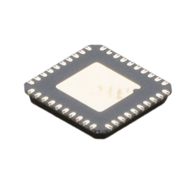


 工商网监
湘ICP备2023018690号
工商网监
湘ICP备2023018690号
